Pairlink Rabbit-B Bluetooth 5 BLE Module User Guide
This document contains information that is proprietary to Pairlink . This document is commercially confidential and must NOT be disclosed to third parties without prior consent. The information provided herein is believed to be reliable. But production testing may not include testing of all parameters. Pairlink reserves the right to change information at any time without notification.
Main Application Domain
- MCU data pass-through.
- 2:Bluetooth Printer / Scanner / Digital price tag etc.
- Remote control / Keyboard and Mouse / Toys / Smart phone self timer etc.
- Industrial remote control / Industrial telemetry / Industrial data collection.
- Smart home / Intelligent lighting / Intelligent access control system.
Electrical Specifications
Absolute Ratings
Parameter | Specification | Unit | |
| Min. | Max. | ||
Power Supply(V) | -0.3V | +3.6V | Burn the module permanently if it exceeds +3.6V |
| Storage temperature(℃) | -55 | +125 | |
Working temperature (℃) | -40 | +85 | |
| ESD HBM | -3.5KV | +3.5KV | Human Body Model |
ESD CDM | -500V | +500V | Charged Device Model |
Recommended Operating Conditions
Parameter | Specification | Note | |||
| Min. | Typical | Max. | |||
| Power Supply(V) | 1.8 | 3.3 | 3.6 | ||
| Communication level(V) | 3.3 | Can’t communicate with 5V TTL level directly | |||
| Working temperature(℃) | -40 | 20 | +85 | Industry Standard | |
| TX Current (mA) | 10.2 | TX Power=+4dBm | |||
| 12.7 | TX Power=+8dBm | ||||
| Consume | RX Current (mA) | 6.8 | VBAT=3V3,1Mbps | ||
| Sleep Current (uA) | 3.8 | Deep-sleep ,Supports GPIO wake-up and timer wake-up | |||
| TX Power(dBm) | +8 | ||||
| Receive Sensitivity(dBm) | -97 | 1Mbps | |||
Digital I/O Characteristic
| Characteristics | Condition | Symbol | Specification | Unit | ||
| Min. | Typical | Max. | ||||
| Input Low Voltage | VIL | – | 0 | 0.9 | V | |
| Input High Voltage | VIH | 2.0 | 3.3 | 3.6 | V | |
| VBAT=3V3 | ||||||
| Output Low Voltage | VOL | 0 | – | 0.33 | V | |
| Output High Voltage | VOH | 2.97 | – | 3.3 | V | |
Hardware Design and PCB layout
Pin assignment and Pin description
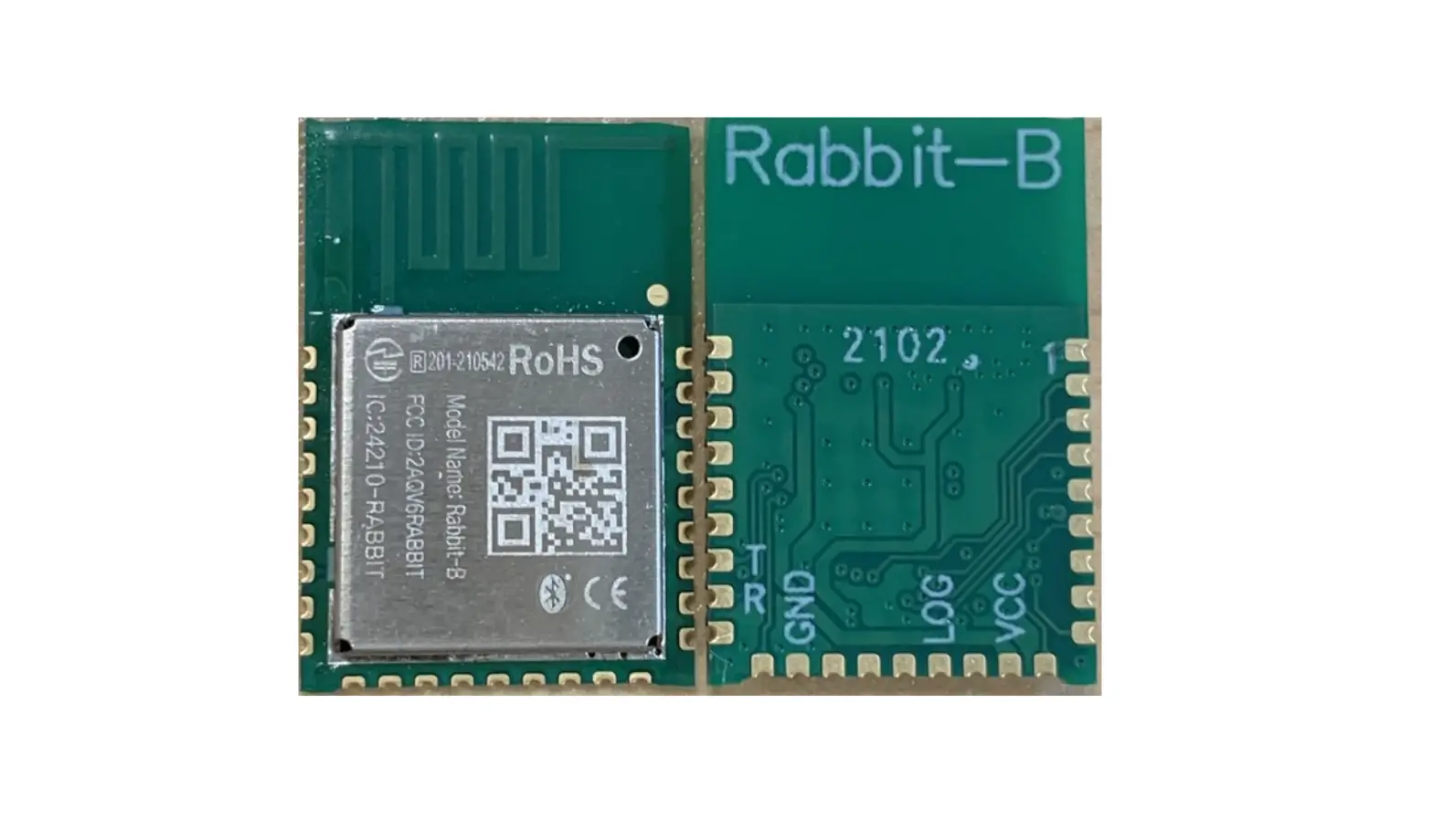
Rabbit-B Pin definition can refer to Figure 1.
| Pin Number | Pin Name | I/O | Alternate Function Description |
| 11 | VBAT | P | Power Supply(DC1.8V~3.6V). |
| 1,17,24,27 | GND | P | Connect to Ground. |
| 12 | RESET | DI | Reset signal (active high). |
| 13 | LOG_OUT | DIO | Log_out,not intended for customer use. |
| 20 | P3_1 | DIO | GPIO/UART_RX |
| 21 | P3_0 | DIO | GPIO/UART_TX |
| 25 | 32K_XI | A | INPUT/OUTPUT with selectable pull up/down resistor. General purpose I/O port bit or alternate function nodes. Contain state retention mechanism during power down. |
| 26 | 32K_XO | A | |
| 2 | P0_0 | DIO | |
| 3 | P0_4 | DIO | |
| 4 | P0_2 | DIO | |
| 5 | P0_1 | DIO | |
| 6 | P4_0 | DIO | |
| 7 | P4_1 | DIO | |
| 8 | P4_2 | DIO | |
| 9 | P4_3 | DIO | |
| 10 | P0_6 | DIO | |
| 14 | P5_0 | DIO | |
| 15 | P1_0 | DIO | |
| 16 | P1_1 | DIO | |
| 18 | P3_2 | DIO | |
| 19 | P2_3 | DIO/AIN | GPIO/ADCIN3 |
| 22 | P2_4 | DIO/AIN | GPIO/ADCIN4 |
| 23 | P2_5 | DIO/AIN | GPIO/ADCIN5 |
Table 1: Module Pin Description
Note: GPIO has integrated pull-up and pull-down resistors.
Support GPIO super multiplexing function, WAKE_UP / UART / SPI / IIC / PWM / and other functions can be arbitrarily configured on GPIO.
For more GPIO function configuration questions, contact to Pairlink.
As shown in the following table: GPIO Pin detailed Information.
| Rabbit-B Rabbit-C Ra bbit-S | GPIO Index | ADC | Hardware Default Pull settingil 00K) Reset state | Rom Code Setting | Pull resistor | Bootc ode Default | Wakeup Function | Dryier current |
| GPIO _O | Pull Down | Pull Down | 10K/100K | Yes | ||||
| P0_1 | GPIO _1 | Pull Down | Pull Down | 10K1OOK | ||||
| P0_2 | GPIO_2 | Pull Down | Pull Down | 10K1OOK | Yes | 8mA | ||
| P0_3 | GPIO_3 | Pull Up | Output High | 10K1100K | LOG UART TX | Yes | 8mA | |
| PO _4 | GPIO _4 | Pull Down | Pull Down | 101(100K | Yes | 8mA | ||
| P0_5 | GPIO_5 | Pull Down | Pull Down | 10W100K | Yes | 8mA | ||
| P0_6 | GPIO _6 | Pull Down | Pull Down | 10K1100K | Yes | 8mA | ||
| P1_0 | GPIO_B | Pull Up | Pull Up | 10K 100K | SWDIO | Yes | 8mA | |
| P1_1 | GPIO_9 | Pull Up | Pull Up | 10K1OOK | SWDCLK | Yes | 8mA | |
| P5_0 | GPIO_25 | Pull Down | Pull Down | 5K50K | Yes | 8mA | ||
| k XI | GPIO_26 | Pull Down | Pull Down | 101(100K | Yes | 8mA | ||
| k X0 | GPIO 27 | Pull Down | Output Low | 10K1100K | Yes | 8mA | ||
| P2 2 | GPIO 18 | ADC/I_PC(channel 2) Differetiall+ | Pull Down | Pull Down | 5K50K | Yes | 8mA | |
| P2 3 | GPIO 19 | ADC/LPC(channel 3) Differatialt- | Pull Down | Pull Down | 5K(50K | Yes | 8mA | |
| P2_4 | GPIO 20 | ADCILPC(channel 4) Differetiat2+ | Pull Down | Pull Down | 5K50K | Yes | 8mA | |
| P2_5 | GPIO 21 | ADCiLPC(channel 5) Differetiat2 | Pull Down | Pull Down | 5Ki’50K | Yes | 8mA | |
| P2_6 | GPIO 22 | ADC(charrel 6) Differetia2+ | Pull Down | Pull Down | 5K150K | Yes | 8mA | |
| P2_7 | GPIO 23 | ADC(charrel T) Differetiat3 | Pull Down | Pull Down | 5K(50K | Yes | 8mA | |
| P3_0 | GPIO 24 | Pull Up | Pull Up | 101(100K | UART TX | `Yes | 8mA | |
| P3_1 | GPIO_25 | Pull Up | Pull Up | 101(100K | UART RX | Yes | 8mA | |
| P3_2 | GPIO_26 | Pull Down | Pull Down | 101(100K | Yes | 8mA | ||
| P3 3 | GPIO 27 | Pull Down | Pull Down | 10K1100K | Yes | 8mA | ||
| P4_0 | GPIO_28 | Pull Down | Pull Down | 101(100K | Yes | 8mA | ||
| P4_1 | GPIO_29 | Pull Down | Pull Down | 10K1100K | Yes | 8mA | ||
| P4_2 | GPIO 30 | Pull Down | Pull Down | 101(100K | Yes | 8mA | ||
| P4 3 | GPIO 31 | Pull Up | Pull Up | 101 100K | Yes | 8mA |
Appearance and Dimensions
Figure 2 shows the size of the module.The components and prominent structure are not allowed put in this size range(20.5mm*14.0mm*2.6mm).
The following land pattern size is recommended for user board design. However, user can modify it according PCB soldering conditions. Sufficient examination is necessary if use the modified land pattern.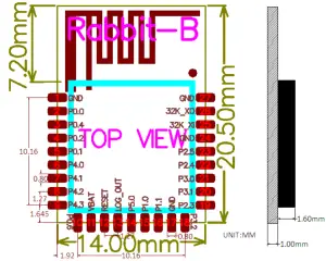
Figure 2: Mechanical Information
Module Layout Guideline
The layout on user PCB should be designed according to the following guideline.
When the module is placed on the PCB, it must be ensured that the RF antenna area (2 times the width of the module) is hollow or suspended, and there must be no traces, vias or copper.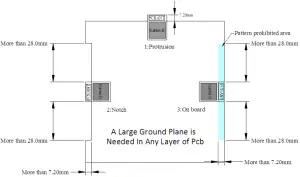
Welding Declaration
The Rabbit-B module only supports one reflow soldering. Our company is not responsible for the module failure caused by multiple reflow soldering.
Figure 3: Reflow Soldering Temperature
| Profile Feature | Sn-Pb Assembly | Pb-Free Assembly |
| Solder Paste | Sn63/Pb37 | Sn96.5/Ag3/Cu0.5 |
| Preheat Temperature min iTsmin ) | 100°C | 150°C |
| Preheat temperature max (Tsmax) | 150°C | 200°C |
| Preheat Time (Tsmin to Tsmax)(ts) | 60-120 sec | 60-120 sec |
| Average ramp-up rate(Tsmax to Tp) | 3°C/second max | 3°C/second max |
| Liquidous Temperature (TL) | 183°C | 217°C |
| Time ( IL ) Maintained Above ) TL) | 60-90 sec | 30-90 sec |
| Peak temperature Tp) | 220-235°C | 230-250°C |
| Aveage ramp-down rate ( Tp to Tsmax ) | 6°C/second max | 6°C/second max |
| Time 25°C to peak temperature | 6 minutes max | 8 minutes max |
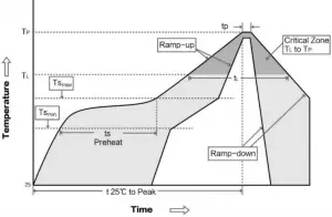
Figure 4: Reflow Soldering Curve
FCC Statement
Federal Communications Commission (FCC) Interference Statement
This equipment has been tested and found to comply with the limits for a Class B digital device, pursuant to Part15 of the FCC Rules.
These limits are designed to provide reasonable protection against harmful interference in a residential installation. This equipment generate, uses and can radiate radio frequency energy and, if not installed and used in accordance with the instructions, may cause harmful interference to radio communications.
However, there is no guarantee that interference will not occur in a particular installation. If this equipment does cause harmful interference to radio or television reception, which can be determined by turning the equipment off and on, the user is encouraged to try to correct the interference by one of the following measures:
- Reorient or relocate the receiving antenna.
- Increase the separation between the equipment and receiver.
- Connect the equipment into an outlet on a circuit different from that to which the receiver is connected.
- Consult the dealer or an experienced radio/TV technician for help.
This device complies with Part 15 of the FCC Rules.
Operation is subject to the following two conditions:
- This device may not cause harmful interference, and
- this device must accept any interference received, including interference that may cause undesired operation.
FCC Caution: Any changes or modifications not expressly approved by the party responsible for compliance could void the user’s authority to operate this equipment.
RF exposure warning
This equipment complies with FCC radiation exposure limits set forth for an uncontrolled environment.
This product may not be collocated or operated in conjunction with any other antenna or transmitter.
Industry Canada (IC)
CAN ICES-003 (B)/NMB-003(B)
This device complies with Industry Canada’s licence-exempt RSSs. Operation is subject to the following two conditions:
- This device may not cause harmful interference, and
- this device must accept any interference received, including interference that may cause undesired operation.
IMPORTANT NOTE
Radiation Exposure Statement:
This equipment complies with IC radiation exposure limits set forth for an uncontrolled environment. This equipment should be installed and operated with minimum distance 20cm between the radiator and your body.
OEM Integration Instructions
This device is intended only for OEM integrators under the following conditions:
The module can be used to installation in other host. The transmitter module may not be co-located with any other transmit or antenna. The module shall be only used with the integral antenna(s) that has been originally tested and certified with this module. As long as 3 conditions above are met, further transmitter test will not be required. However, the OEM integrator is still responsible for testing their end-product for any additional compliance requirement with this module installed (for example, digital device emission, PC peripheral requirements, etc.). OEM integrator is responsible for ensuring the end-user has no manual instruction to remove or install module.
IMPORTANT NOTE
In the event that these conditions cannot be met (for example certain laptop configuration or co-location with another transmitter), then the FCC authorization for this module in combination with the host equipment is no longer considered valid and the FCC ID of the module cannot be used on the final product. In these and circumstance, the OEM integrator will be responsible for re-evaluating. The end product (including the transmitter) and obtaining a separate FCC authorization. The final end product must be labeled in a visible area with the following: “Contains Transmitter Module FCC ID: 2AQV6RABBIT”.
Antenna Specification:
Antenna Type | Manufacturer | Frequency Range (MHz) | Maximum Peak Antenna Gain(dBi) |
PCB Antenna | N/A | 2402 – 2480 | -0.41dBi |
IMPORTANT NOTE:
This Module (IC: 24210-RABBIT) has been approved by Industry Canada to operate with the antenna types listed below with the maximum permissible gain indicated. Antenna types not included in this list, having a gain greater than the maximum gain indicated for that type, are strictly prohibited for use with this device.
The Host Marketing Name (HMN) must be displayed (according to e-labelling requirements) or indicated at any location on the exterior of the host product or product packaging or product literature, which shall be available with the host product or online.
The host product shall be properly labelled to identify the modules within the host product. The Innovation, Science and Economic Development Canada certification label of a module shall be clearly visible at all times when installed in the host product; otherwise, the host product must be labelled to display the Innovation, Science and Economic Development Canada certification number for the module, preceded by the word “Contains” or similar wording expressing the same meaning, as follows: Contains IC: 24210-RABBIT
Antenna Specification
| Antenna Type | Manufacturer | Frequency Range (MHz) | Maximum Peak Antenna Gain(dBi) |
| PCB Antenna | N/A | 2402 – 2480 | -0.41 |


