Focalcrest IEC-EDGE2-0432 Single Board Computer 
Introduction
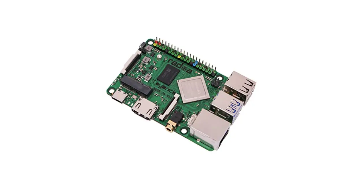
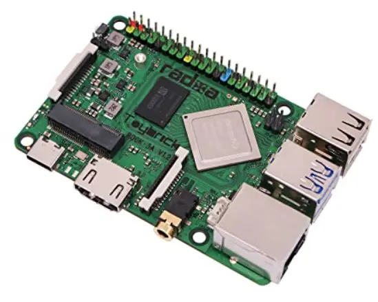
Product Description
Edge 2 is a high-performance and rich-interface ARM64 single-board computer targeted for a wide range of IoT networking and computing applications. It may apply in networking, computing, controlling, and home entertainment areas for further achievement with the help of multipurpose software. The single-board computer combines a MIXTILE System-on-Module Core 3568, a WLAN+BT wireless module, and plenty of expansion interfaces.
Package list
- 1x MIX TILE Edge 2 with customizable shell
- 1x 1m type-c to type-c cable
- 2x 16mm 6dbi 2.4G/5.8G Antennas
Main Features
- Quad-core Cortex-A55 SoC Processor RK3568 up to 2.0GHz
- 2/4GBytes LPDDR4 SDRAM Memory
- 16/32GBytes eMMC Flash Memory
- 0.8 Tops NPU
- Wi-Fi 6 802.11ax
- Dual-Mode Bluetooth 5.0
- Support 4G/5G/LoRa/Zigbee module
- 1x Gigabit Ethernet Port
- 1x MicroSD 3.0 Flash Expansion Socket
- 3x USB 2.0/3.0 ports up to 5Gbps
- 1x M.2 Socket: PCIe 3.0, USB 3.0, SIM Socket
- 1x Mini-PCIe Socket: USB2.0, SIM Socket
- 1 x U.2 Socket: SATA/PCIe, SATA, RGMII/SPI/I2S, USB2.0
- 1x HDMI2.0, 1x eDP, 2x MIPI-DSI, and 1x MIPI-CSI
- 4KP60 H.265/H.264/VP9 video decoder
- 1080P100 H.264/H.265 video encoder
- 1x RS485, 1x CAN, 1x I2C, and 2x UART
- 3x PDM, 1x SPDIF, 1x Speaker, 1x IR, and 4x ADC
- Real Time Clock with Battery Backup
- 2x power supply ports:
- Type-C PD3.0 Power input (Max 3A @ 20V)
- 12V DC/SATA Power input (Max 3A)
- Android 11 Board Support Package
- 0 to +80°C Operating Temperature
Key Component Specifications
The key component specifications are described below with relevant hardware information and developing notices. For more information, pin assignments and signal descriptions are listed in Chapter 2, Connectors & Pin Assignments.
MIXTILE Core 3568
The Core 3568 is a System-on-Module that expands all CPU functions to pins with an innovative connector. The Rockchip RK3568 ARM64 CPU contains many peripherals to support multi-purpose.
- Quad Cortex-A55 processing cores
- Core operating frequencies up to 2.0GHz
- Neural Process Unit with processing performance up to 0.8 TOPS
- Support 4k@60fps H.265/H.264/VP9 decoder; 1080P@100fps H.265/H.264 encoder
- LPDDR4 SDRAM supports up to 8GB The SDRAM is 32bits data width, 4 ranks LPDDR4 memory capacities from 2GBytes to 8GBytes. The system flash memory supports eMMC 5.1 memory capacities from 16GBytes to 256GBytes. The default memory setting is 2/4GBytes LPDDR4 and 16/32GBytes eMMC for Edge 2.
Wi-Fi 6 / Bluetooth
Edge 2 integrates a Wi-Fi and Bluetooth module AP6275S, that can wake up the device from sleep mode. AP6275S supports Wi-Fi 6 and dual-mode Bluetooth 5.0 that could interact with different vendors’ 802.11a/b/g/n/ac/ax 2×2 Access Points with MIMO standard and can accomplish up to a speed of 1200Mbps with the dual-stream. Wi-Fi wake and enable signals connect to GPIO0 in the processor, which can be operating while the device is sleep.
MicroSD Socket
The MicroSD socket accepts standard 11mm x 15mm Micro-SD cards with capacities up to 64GBytes. The 4bits data interface supports the SDMMC3.0 protocol. The default boot setting is the eMMC Flash which can change to the MicroSD card.
M.2 Socket
M.2, Next Generation Form Factor (NGFF), is specified for expansion modules. The M.2 interface uses a standard 75 pins B key socket, which supports USB3.0-based WWAN modules, PCIe-based WWAN modules, and PCIe-based SSD modules. The M.2 socket supports the module sizes of 2242, 3042, and 3052. The module supporting configuration, including power, reset, and interrupt signals, is under software control by Core 3568. Since each module needs specific configuration definitions, check the configuration setting before connecting the module.
SIM Support
The M.2 socket includes a SIM socket with the SIM_M.2 mark, which supports 12mm x 15mm micro-SIM cards for 4G/5G cellular function. This socket does not support dual SIM.
USB Support
The M.2 socket supports one standard USB 3.0 interface. Since the USB 3.0 data signals and one lane of PCIe data signals are using the same set of pins, a GPIO is used to select USB 3.0 and a lane of two-lane PCIe 3.0 signal.
PCIe Support
The M.2 socket supports a two-lane PCIe 3.0 interface. Edge 2 uses PI6C557-03BLE as a clock generator to provide a 100MHz clock signal for the CPU and M.2 socket. For full functioning of the two-lane PCIe signal, the selecting GPIO, PCIE_USB_SEL_GPIO1_D0, needs to set LOW to active.
Mini-PCIe Socket
The mini-PCIe is a small form factor PCI card interface, which uses a standard 52 pins mini-PCIe socket. It contains a USB 2.0 interface with a supported SIM signal. The mini-PCIe socket supports the module sizes of 3052.
The module supporting configuration, including power, reset, and interrupt signals, is under software control by Core 3568. Since each module needs specific configuration definitions, check the configuration setting before connecting the module.
SIM Support
The mini-PCIe socket includes a SIM socket with SIM_Mini mark, which supports 12mm x 15mm micro-SIM cards for 4G cellular function. This socket does not support dual SIM.
USB Support
The mini-PCIe socket supports a standard USB 2.0 interface.
Gigabit Ethernet
The IEEE802.3 compliant ethernet supports 10/100/1000Mb half-duplex and full-duplex auto-negotiation. The GbE communicates to an external PHY, RTL8211F-CG, through an RGMII interface from the processor. The RJ45 connector contains status and speed lights. The green light is on for connection and flashing for data transmitting. The yellow light is on for 1000Mbps and off for 10/100Mbps.
Power Input
Power Delivery (PD)
The power port uses a USB-C port, which supports USB PD 3.0 . An on-board Power Delivery controller allows the maximum power input of 20V @ 3A. The Edge 2, as device mode, can be communicated by USB-C, which supports USB 2.0 for ADB debugging, firmware update. 12V DC DC power inputs from a DC power jack socket or a SATA power socket require 12V @ 3A.
USB 2.0/3.0 Host Ports
Edge 2 has three standard USB 2.0/3.0 host ports using type-A connectors and one USB 2.0/3.0 port connects M.2 socket. These USB 2.0/3.0 ports are provided by a USB 3.0 hub, VL817. The three type-A connectors support 5V at 1A power and dependent software power dis/enabling.
RS485
RS485 connector has three pins, pin A, B, and GND for communication. RS485 connects to UART4 in CPU via interface IC, SP485REN-L. RS485 is a half-duplex bus with a default setting on receiving state. It will automatically switch to the sending state when needed. RS485 uses full isolation designs, the power supply and ground are isolated from the module used in the board, and the signal is isolated by an optocoupler.
Display Support
The video output processor supports the resolution from 1920×1080@60Hz to 4096×2304@60Hz and three simultaneous displays in the following interfaces. The default main display is HDMI.
HDMI
HDMI display compliant HDMI 1.4 and HDMI 2.0. It supports up to 1920×1080@120Hz and 4096×2304@60Hz resolution.
eDP
The eDP display supports up to 2560×1600@60Hz resolution, up to 4 lanes of 2.7Gbps/lane. The 30-pin FPC connector includes the eDP interface and a backlight source. The pin assignments are listed in the next chapter.
MIPI-DSI
The MIPI-DSI display supports two-channel DSI and 2.5Gbps maximum data rate per lane. It supports up to 1920×1080@60Hz display output for single-MIPI mode and 2560×1440@60Hz for dual-MIPI mode. Two MIPI-DIS interfaces use 30-pin FPC connectors, MIPI-DSI0 and MIPI-DSI1, which include one channel MIPI-DSI and one touch panel signal (TP). The connectivity is show in the following figure:
U.2 Connector
The U.2 interface uses a 68-pin U.2 connector including a standard SATA signal, which supports 5V at 3A maximum, a SATA 3.0/PCIe 2.0 signal, a USB 2.0 signal, and another set of RGMII for ethernet.
Buttons & LEDs
The POWER button controls three statuses of the device, on, off, and sleep. Short press POWER button to turn on device when the device is off, press and hold POWER button to turn off device. Short press POWER button to enter sleep mode when the device is on. Short press RESET button to reset the device. When the device is on, press the RECOVERY button and hold, it will restart and restore the factory settings. The MASK ROM button is for development only, hold the MASKROM button and power up (or reset). The system will enter MaskROM mode for firmware development.The power and system LEDs indicate the statuses of the power supply and system operating. And two small LEDs on the front side of board indicate the network status of M.2 and mini-PCIe modules.
Connectors & Pin Assignments
The following section lists the interfaces connector pin assignments, pin types with corresponding signal descriptions. The interface connectors on Edge 2 are listed in the table below.
Debug
| Pin # | Pin Name | Pin Type | Input/ Output | Signal Description |
| 1 | UART2_RXD | IO | Input | UART2 serial data input for debug |
| 2 | UART2_TXD | IO | Output | UART2 serial data output for debug |
| 3 | GND | GND | – | Ground |
UART
| Pin # | Pin Name | Pin Type | Input/ Output | Signal Description |
| 1 | 3.3V | PWR | Output | 3.3V @ 100mA Max |
| 2 | UART3_RX | IO | Input | UART3 serial data input |
| 3 | UART3_TX | IO | Output | UART3 serial data output |
| 4 | GND | GND | – | Ground |
| Pin # | Pin Name | Pin Type | Input/ Output | Signal Description |
| 1 | 3.3V | PWR | Output | 3.3V @ 100mA Max |
| 2 | UART5_RX | IO | Input | UART5 serial data input |
| 3 | UART5_TX | IO | Output | UART5 serial data output |
| 4 | GND | GND | – | Ground |
CAN-IO
| Pin # | Pin Name | Pin Type | Input/ Output | Signal Description |
| 1 | 5V | PWR | Output | 5V @ 200mA Max |
| 2 | CAN1_RX | IO | Input | CAN receive data, connect to CAN transceiver |
| 3 | CAN1_TX | IO | Output | CAN transmit data, connect to CAN transceiver |
| 4 | GND | GND | – | Ground |
I2C
| Pin # | Pin Name | Pin Type | Input/ Output | Signal Description |
| 1 | 3.3V | PWR | Output | 3.3V @ 100mA Max |
| 2 | I2C3_SCL | IO | Output | I2C clock signal |
| 3 | I2C3_SDA | IO | I/O | I2C data signal |
| 4 | GND | GND | – | Ground |
5V Output
| Pin # | Pin Name | Pin Type | Input/ Output | Signal Description |
| 1 | 5V | PWR | Output | 5V @ 2A Max in total |
| 2 | 5V | PWR | Output | 5V @ 2A Max in total |
| 3 | GND | GND | – | Ground |
| 4 | GND | GND | – | Ground |
Power button connector
| Pin # | Pin Name | Pin Type | Input/ Output | Signal Description |
| 1 | PWRON_CON | IO | Input | Active-low, same as PWR button |
| 2 | GND | GND | – | Ground |
Reset button connector
| Pin # | Pin Name | Pin Type | Input/ Output | Signal Description |
| 1 | RESET_KEY | IO | Input | Active-low reset signal, same as RESET button |
| 2 | GND | GND | – | Ground |
SPDIF
| Pin # | Pin Name | Pin Type | Input/ Output | Signal Description |
| 1 | SPDIF_TX | IO | Output | SPDIF output signal |
| 2 | 3.3V | PWR | Output | 3.3V @ 100mA Max |
| 3 | GND | GND | – | Ground |
RS485
| Pin # | Pin Name | Pin Type | Input/ Output | Signal Description |
| 1 | GND | GND | – | Ground |
| 2 | 485B | DS | I/O | RS485 differential signal Negative |
| 3 | 485A | DS | I/O | RS485 differential signal Positive |
ADC
| Pin # | Pin Name | Pin Type | Input/ Output | Signal Description |
| 1 | 3.3V | PWR | Output | 3.3V @ 100mA Max |
| 2 | SARADC_VIN4 | ANA | Input | ADC analog signal |
| 3 | SARADC_VIN5 | ANA | Input | ADC analog signal |
| 4 | SARADC_VIN6 | ANA | Input | ADC analog signal |
| 5 | SARADC_VIN7 | ANA | Input | ADC analog signal |
| 6 | GND | GND | – | Ground |
Speaker
| Pin # | Pin Name | Pin Type | Input/ Output | Signal Description |
| 1 | SPK+ | ANA | Output | speaker driver output Positive |
| 2 | SPK- | ANA | Output | speaker driver output Negative |
DMIC
| Pin # | Pin Name | Pin Type | Input/ Output | Signal Description |
| 1 | 3.3V | PWR | Output | 3.3V @ 500mA Max in total |
| 2 | 3.3V | PWR | Output | 3.3V @ 500mA Max in total |
| 3 | GND | GND | – | Ground |
| 4 | GND | GND | – | Ground |
| 5 | PDM_SDI1 | IO | Input | PDM data signal |
| 6 | PDM_SDI2 | IO | Input | PDM data signal |
| 7 | PDM_SDI3 | IO | Input | PDM data signal |
| 8 | GND | GND | – | Ground |
| 9 | PDM_CLK1 | IO | Output | PDM clock signal |
| 10 | GND | GND | – | Ground |
MIPI-DSI0
| Pin # | Pin Name | Pin Type | Input/ Output | Signal Description |
| 1 | GND | GND | – | Ground |
| 2 | MIPI_DSI_TX0_D0N | LVDS | Output | MIPI-DSI0 data signal Negative |
| 3 | MIPI_DSI_TX0_D0P | LVDS | Output | MIPI-DSI0 data signal Positive |
| 4 | GND | GND | – | Ground |
| 5 | MIPI_DSI_TX0_D1N | LVDS | Output | MIPI-DSI0 data signal Negative |
| 6 | MIPI_DSI_TX0_D1P | LVDS | Output | MIPI-DSI0 data signal Positive |
| 7 | GND | GND | – | Ground |
| 8 | MIPI_DSI_TX0_CLKN | LVDS | Output | MIPI-DSI0 clock signal Negative |
| 9 | MIPI_DSI_TX0_CLKP | LVDS | Output | MIPI-DSI0 clock signal Positive |
| 10 | GND | GND | – | Ground |
| 11 | MIPI_DSI_TX0_D2N | LVDS | Output | MIPI-DSI0 data signal Negative |
| 12 | MIPI_DSI_TX0_D2P | LVDS | Output | MIPI-DSI0 data signal Positive |
| 13 | GND | GND | – | Ground |
| 14 | MIPI_DSI_TX0_D3N | LVDS | Output | MIPI-DSI0 data signal Negative |
| 15 | MIPI_DSI_TX0_D3P | LVDS | Output | MIPI-DSI0 data signal Positive |
| 16 | GND | GND | – | Ground |
| 17 | LCD0_BL_PWM4 | IO | Output | PWM Output for backlight adjust |
| 18 | NC | – | – | Not connected pin |
| 19 | 3.3V | PWR | Output | 3.3V @ 200mA Max |
| 20 | LCD0_RST_L_GPIO1_D1 | IO | Output | GPIO output for lcd reset |
| 21 | SARADC_VIN2_LCD_ID | ANA | Input | Analog signal Input |
| 22 | LCD0_PWREN_H_GPIO0_C7 | IO | Output | GPIO output for lcd power on |
| 23 | I2C1_SCL_TP | IO | Output | I2C clock signal for touch panel |
| 24 | I2C1_SDA_TP | IO | I/O | I2C data signal for touch panel |
| 25 | TP_INT_L_GPIO0_B5 | IO | Input | GPIO for touch panel interrupt |
| 26 | TP_RST_L_GPIO0_B6 | IO | Output | GPIO for touch panel reset |
| 27 | GND | GND | – | Ground |
| 28 | 5V | PWR | Output | 5V @ 500mA Max in total |
| 29 | 5V | PWR | Output | 5V @ 500mA Max in total |
| 30 | 5V | PWR | Output | 5V @ 500mA Max in total |
MIPI-DSI1
| Pin # | Pin Name | Pin Type | Input/ Output | Signal Description |
| 1 | GND | GND | – | Ground |
| 2 | MIPI_DSI_TX1_D0N | LVDS | Output | MIPI-DSI1 data signal Negative |
| 3 | MIPI_DSI_TX1_D0P | LVDS | Output | MIPI-DSI1 data signal Positive |
| 4 | GND | GND | – | Ground |
| 5 | MIPI_DSI_TX1_D1N | LVDS | Output | MIPI-DSI1 data signal Negative |
| 6 | MIPI_DSI_TX1_D1P | LVDS | Output | MIPI-DSI1 data signal Positive |
| 7 | GND | GND | – | Ground |
| 8 | MIPI_DSI_TX1_CLKN | LVDS | Output | MIPI-DSI1 clock signal Negative |
| 9 | MIPI_DSI_TX1_CLKP | LVDS | Output | MIPI-DSI1 clock signal Positive |
| 10 | GND | GND | – | Ground |
| 11 | MIPI_DSI_TX1_D2N | LVDS | Output | MIPI-DSI1 data signal Negative |
| 12 | MIPI_DSI_TX1_D2P | LVDS | Output | MIPI-DSI1 data signal Positive |
| 13 | GND | GND | – | Ground |
| 14 | MIPI_DSI_TX1_D3N | LVDS | Output | MIPI-DSI1 data signal Negative |
| 15 | MIPI_DSI_TX1_D3P | LVDS | Output | MIPI-DSI1 data signal Positive |
| 16 | GND | GND | – | Ground |
| 17 | PWM5 | IO | Output | PWM Output for backlight adjust |
| 18 | NC | – | – | Not connected pin |
| 19 | 3.3V | PWR | Output | 3.3V @ 200mA Max |
| 20 | LCD1_RST_L_GPIO3_B6 | IO | Output | GPIO output for lcd reset |
| 21 | SARADC_VIN2_LCD_ID | ANA | Input | Analog signal Input |
| 22 | LCD1_PWREN_H_GPIO4_D2 | IO | Output | GPIO output for lcd power enable |
| 23 | I2C1_SCL_TP | IO | Output | I2C clock signal for touch panel |
| 24 | I2C1_SDA_TP | IO | I/O | I2C data signal for touch panel |
| 25 | TP_INT_L_GPIO0_B5 | IO | Input | GPIO for touch panel interrupt |
| 26 | TP_RST_L_GPIO0_B6 | IO | Output | GPIO for touch panel reset |
| 27 | GND | GND | – | Ground |
| 28 | 5V | PWR | Output | 5V @ 500mA Max in total |
| 29 | 5V | PWR | Output | 5V @ 500mA Max in total |
| 30 | 5V | PWR | Output | 5V @ 500mA Max in total |
eDP
| Pin # | Pin Name | Pin Type | Input/ Output | Signal Description |
| 1 | GND | GND | – | Ground |
| 2 | EDP_TX_D1N | LVDS | Output | EDP data signal Negative |
| 3 | EDP_TX_D1P | LVDS | Output | EDP data signal Positive |
| 4 | GND | GND | – | Ground |
| 5 | EDP_TX_D0N | LVDS | Output | EDP data signal Negative |
| 6 | EDP_TX_D0P | LVDS | Output | EDP data signal Positive |
| 7 | GND | GND | – | Ground |
| 8 | EDP_TX_AUXN_CON | LVDS | Output | EDP clock signal Negative |
| 9 | EDP_TX_AUXP_CON | LVDS | Output | EDP clock signal Positive |
| 10 | GND | GND | – | Ground |
| 11 | EDP_TX_D2N | LVDS | Output | EDP data signal Negative |
| 12 | EDP_TX_D2P | LVDS | Output | EDP data signal Positive |
| 13 | GND | GND | – | Ground |
| 14 | EDP_TX_D3N | LVDS | Output | EDP data signal Negative |
| 15 | EDP_TX_D3P | LVDS | Output | EDP data signal Positive |
| 16 | 3.3V | PWR | Output | 3.3V @ 500mA Max in total |
| 17 | 3.3V | PWR | Output | 3.3V @ 500mA Max in total |
| 18 | GND | GND | – | Ground |
| 19 | GND | GND | – | Ground |
| 20 | EDP_HPD_GPIO0_C2 | IO | Input | eDP hot plug detect signal |
| 21 | GND | GND | – | Ground |
| 22 | GND | GND | – | Ground |
| 23 | GND | GND | – | Ground |
| 24 | GND | GND | – | Ground |
| 25 | EDP_BL_EN_GPIO3_C1 | IO | Output | Output for enable backlight power |
| 26 | EDP_PWM12_GPIO4_C5 | IO | Output | PWM Output for backlight adjust |
| 27 | GND | GND | – | Ground |
| 28 | 12V | PWR | Output | 12V power supply for backlight |
| 29 | 12V | PWR | Output | 12V power supply for backlight, |
| 30 | 12V | PWR | Output | 12V power supply for backlight |
Camera
| Pin # | Pin Name | Pin Type | Input/ Output | Signal Description |
| 1 | GND | GND | – | Ground |
| 2 | MIPI_CSI_RX_D0N | LVDS | Input | MIPI_CSI data signal Negative |
| 3 | MIPI_CSI_RX_D0P | LVDS | Input | MIPI_CSI data signal Positive |
| 4 | GND | GND | – | Ground |
| 5 | MIPI_CSI_RX_D1N | LVDS | Input | MIPI_CSI data signal Negative |
| 6 | MIPI_CSI_RX_D1P | LVDS | Input | MIPI_CSI data signal Positive |
| 7 | GND | GND | – | Ground |
| 8 | MIPI_CSI_RX_CLK0N | LVDS | Input | MIPI_CSI clock signal Negative |
| 9 | MIPI_CSI_RX_CLK0P | LVDS | Input | MIPI_CSI clock signal Positive |
| 10 | GND | GND | – | Ground |
| 11 | MIPI_CSI_RX_D2N | LVDS | Input | MIPI_CSI data signal Negative |
| 12 | MIPI_CSI_RX_D2P | LVDS | Input | MIPI_CSI data signal Positive |
| 13 | GND | GND | – | Ground |
| 14 | MIPI_CSI_RX_D3N | LVDS | Input | MIPI_CSI data signal Negative |
| 15 | MIPI_CSI_RX_D3P | LVDS | Input | MIPI_CSI data signal Positive |
| 16 | GND | GND | – | Ground |
| 17 | CIF_CLKOUT | IO | Output | CLOCK output for camera |
| 18 | GND | GND | – | Ground |
| 19 | NC | – | – | Not connected pin |
| 20 | CAMERA0_RST_L_GPIO4_B5 | IO | Output | GPIO output for camera reset |
| 21 | CAMERA0_PDN_L_GPIO4_B4 | IO | Output | GPIO output for camera disable |
| 22 | CAMERA0_PWREN_GPIO1_D4 | IO | Output | GPIO output for camera enable |
| 23 | I2C4_SCL_M0 | IO | Output | I2C clock signal |
| 24 | I2C4_SDA_M0 | IO | Input | I2C data signal |
| 25 | PWM14_M0 | IO | Output | PWM Output signal |
| 26 | GND | GND | – | Ground |
| 27 | GND | GND | – | Ground |
| 28 | 5V | PWR | Output | 5V @ 500mA Max in total |
| 29 | 5V | PWR | Output | 5V @ 500mA Max in total |
| 30 | 5V | PWR | Output | 5V @ 500mA Max in total |
| 31 | GND | GND | – | Ground |
| 32 | NC | – | – | Not connected pin |
| 33 | NC | – | – | Not connected pin |
| 34 | NC | – | – | Not connected pin |
| 35 | GND | GND | – | Ground |
| 36 | MIPI_MCLK1 | IO | Output | CLOCK output for camera |
| 37 | GND | GND | – | Ground |
| 38 | MIPI_CSI_RX_CLK1N | LVDS | Input | MIPI_CSI clock signal Negative |
| 39 | MIPI_CSI_RX_CLK1P | LVDS | Input | MIPI_CSI clock signal Positive |
| 40 | GND | GND | – | Ground |
M.2
| Pin # | Pin Name | Pin Type | Input/ Output | Signal Description |
| 1 | NC | – | – | Not connected pin |
| 2 | 3.8V | PWR | Output | 3.8V @ 3A Max in total |
| 3 | GND | GND | – | Ground |
| 4 | 3.8V | PWR | Output | 3.8V @ 3A Max in total |
| 5 | GND | GND | – | Ground |
| 6 | M2_ONOFF_GPIO1_D2 | IO | Output | GPIO output for on or off to module |
| 7 | HUB_HOST3_DP | LVDS | I/O | USB2.0 data signal Positive |
| 8 | NC | – | – | Not connected pin |
| 9 | HUB_HOST3_DM | LVDS | I/O | USB2.0 data signal Negative |
| 10 | M2_LED1 | IO | Input | Connect negative for network status |
| 11 | GND | GND | – | Ground |
| 20 | NC | – | – | Not connected pin |
| 21 | NC | – | – | Not connected pin |
| 22 | NC | – | – | Not connected pin |
| 23 | M2_WAKE_GPIO0_B7 | IO | Input | GPIO for module to wakeup CPU |
| 24 | NC | – | – | Not connected pin |
| 25 | NC | – | – | Not connected pin |
| 26 | NC | – | – | Not connected pin |
| 27 | GND | GND | – | Ground |
| 28 | NC | – | – | Not connected pin |
| 29 | PCIE30_TX1_N/HUB_USB3_SSTXN | LVDS | Output | PCIE3.0/USB3.0 data signal Negative |
| 30 | M2_UIM_RESET | IO | Input | Reset signal to SIM socket |
| 31 | PCIE30_TX1_P/HUB_USB3_SSTXP | LVDS | Output | PCIE3.0/USB3.0 data signal Positive |
| 32 | M2_UIM_CLK | IO | Input | Clock signal to SIM socket |
| 33 | GND | GND | – | Ground |
| 34 | M2_UIM_DATA | IO | Input | data signal to SIM socket |
| 35 | PCIE30_RX1N/HUB_USB3_SSRXN | LVDS | Input | PCIE3.0/USB3.0 data signal Negative |
| 36 | M2_UIM_PWR | IO | Input | power to SIM socket |
| 37 | PCIE30_RX1P/HUB_USB3_SSRXP | LVDS | Input | PCIE3.0/USB3.0 data signal Positive |
| 38 | NC | – | – | Not connected pin |
| 39 | GND | GND | – | Ground |
| 40 | NC | – | – | Not connected pin |
| 41 | PCIE30_TX0_N | LVDS | Output | PCIE3.0 data signal output Negative |
| 42 | NC | – | – | Not connected pin |
| 43 | PCIE30_TX0_P | LVDS | Output | PCIE3.0 data signal output Positive |
| 44 | NC | – | – | Not connected pin |
| 45 | GND | GND | – | Ground |
| 46 | NC | – | – | Not connected pin |
| 47 | PCIE30_RX0N | LVDS | Input | PCIE3.0 data signal input Negative |
| 48 | NC | – | – | Not connected pin |
| 49 | PCIE30_RX0P | LVDS | Input | PCIE3.0 data signal input Positive |
| 50 | PCIE30X2_PERSTN_M1 | IO | Output | PCIe warm reset request |
| 51 | GND | GND | – | Ground |
| 52 | PCIE30X2_CLKREQN_M1 | IO | Input | clock request from PCIe peripheral |
| 53 | CLK0N_CON | LVDS | Output | PCIE3.0 clock signal output Negative |
| 54 | PCIE30X2_WAKEN_M1 | IO | Input | PCIe wake up |
| 55 | CLK0P_CON | LVDS | Output | PCIE3.0 clock signal output Positive |
| 56 | NC | – | – | Not connected pin |
| 57 | GND | GND | – | Ground |
| 58 | NC | – | – | Not connected pin |
| 59 | NC | – | – | Not connected pin |
| 60 | NC | – | – | Not connected pin |
| 61 | NC | – | – | Not connected pin |
| 62 | NC | – | – | Not connected pin |
| 63 | NC | – | – | Not connected pin |
| 64 | NC | – | – | Not connected pin |
| 65 | NC | – | – | Not connected pin |
| 66 | M2_SIM_DETECT | IO | Output | Card detect signal to SIM socket |
| 67 | M2_RESET_GPIO3_B5 | IO | Output | GPIO output for reset to module |
| 68 | CLK32K_OUT0 | IO | Output | Clock output 32.768K to module |
| 69 | NC | – | – | Not connected pin |
| 70 | 3.8V | PWR | Output | 3.8V @ 3A Max in total |
| 71 | GND | GND | – | Ground |
| 72 | 3.8V | PWR | Output | 3.8V @ 3A Max in total |
| 73 | GND | GND | – | Ground |
| 74 | 3.8V | PWR | Output | 3.8V @ 3A Max in total |
| 75 | NC | – | – | Not connected pin |
Mini-PCIe
| Pin # | Pin Name | Pin Type | Input/ Output | Signal Description |
| 1 | WAKEUP_MINIPCIE_GPIO0_C1 | IO | Input | GPIO for module to wakeup CPU |
| 2 | 3.8V | PWR | Output | 3.8V @ 3A Max in total |
| 3 | NC | – | – | Not connected pin |
| 4 | GND | GND | – | Ground |
| 5 | NC | – | – | Not connected pin |
| 6 | NC | – | – | Not connected pin |
| 7 | NC | – | – | Not connected pin |
| 8 | UIM_PWR | PWR | Input | SIM power supply |
| 9 | GND | GND | – | Ground |
| 10 | UIM_DATA | IO | Input | SIM data signal |
| 11 | NC | – | – | Not connected pin |
| 12 | UIM_CLK | IO | Input | SIM clock signal |
| 13 | NC | – | – | Not connected pin |
| 14 | UIM_RESET | IO | Input | SIM reset signal |
| 15 | GND | GND | – | Ground |
| 16 | NC | – | – | Not connected pin |
| 17 | NC | – | – | Not connected pin |
| 18 | GND | GND | – | Ground |
| 19 | NC | – | – | Not connected pin |
| 20 | NC | – | – | Not connected pin |
| 21 | GND | GND | – | Ground |
| 22 | MiniPCIE_reset_GPIO3_D4 | IO | Output | GPIO output for reset to module |
| 23 | NC | – | – | Not connected pin |
| 24 | 3.8V | PWR | Output | 3.8V @ 3A Max in total |
| 25 | NC | – | – | Not connected pin |
| 26 | GND | GND | – | Ground |
| 27 | GND | GND | – | Ground |
| 28 | NC | – | – | Not connected pin |
| 29 | GND | GND | – | Ground |
| 30 | NC | – | – | Not connected pin |
| 31 | NC | – | – | Not connected pin |
| NC | NC | – | – | Not connected pin |
| 33 | NC | – | – | Not connected pin |
| 34 | GND | GND | – | Ground |
| 35 | GND | GND | – | Ground |
| 36 | USB2_HOST2_DM | LVDS | I/O | USB2.0 data signal Negative |
| 37 | NC | – | – | Not connected pin |
| 38 | USB2_HOST2_DP | LVDS | I/O | USB2.0 data signal Positive |
| 39 | 3.8V | PWR | Output | 3.8V @ 3A Max in total |
| 40 | GND | GND | – | Ground |
| 41 | 3.8V | PWR | Output | 3.8V @ 3A Max in total |
| 42 | LED | IO | Input | System status LED |
| 43 | NC | – | – | Not connected pin |
| 44 | SIM_DETECT | IO | Output | SIM detect |
| 45 | NC | – | – | Not connected pin |
| 46 | NC | – | – | Not connected pin |
| 47 | NC | – | – | Not connected pin |
| 48 | NC | – | – | Not connected pin |
| 49 | NC | – | – | Not connected pin |
| 50 | GND | GND | – | Ground |
| 51 | NC | – | – | Not connected pin |
| 52 | 3.8V | PWR | Output | 3.8V @ 3A Max in total |
U.2
| Pin # | Pin Name | Pin Type | Input/ Output | Signal Description |
| 1 | GND | GND | – | Ground |
| 2 | SATA0_SSRXP | LVDS | Input | SATA data signal input Positive |
| 3 | SATA0_SSRXN | LVDS | Input | SATA data signal input Negative |
| 4 | GND | GND | – | Ground |
| 5 | SATA0_SSTXN | LVDS | Output | SATA data signal output Negative |
| 6 | SATA0_SSTXP | LVDS | Output | SATA data signal output Positive |
| 7 | GND | GND | – | Ground |
| 8 | GMAC0_TXEN | IO | Output | RGMII signal |
| 9 | GMAC0_RXD2 | IO | Input | RGMII signal |
| 10 | NC | – | – | Not connected pin |
| 11 | GMAC0_RXD3 | IO | Input | RGMII signal |
| 12 | GMAC0_RXD0 | IO | Input | RGMII signal |
| 13 | GMAC0_RXD1 | IO | Input | RGMII signal |
| 14 | NC | – | – | Not connected pin |
| 15 | I2C3_SCL_M0 | IO | Output | I2C clock signal |
| 16 | I2C3_SDA_M0 | IO | I/O | I2C data signal |
| 17 | GND | GND | – | Ground |
| 18 | GND | GND | – | Ground |
| 19 | GND | GND | – | Ground |
| 20 | 5V | PWR | Output | 5V @ 3A Max |
| 21 | 5V | PWR | Output | 5V @ 3A Max |
| 22 | 5V | PWR | Output | 5V @ 3A Max |
| 23 | GND | GND | GND | Ground |
| 24 | NC | – | – | Not connected pin |
| 25 | GND | GND | – | Ground |
| 26 | NC | – | – | Not connected pin |
| 27 | NC | – | – | Not connected pin |
| 28 | NC | – | – | Not connected pin |
| 29 | SATA0_LED | IO | Output | SATA0 status for LED |
| 30 | SATA2_LED | IO | Output | SATA2 status for LED |
| 31 | GMAC0_MCLKINOUT | IO | I/O | CLOCK output 125MHz for GMAC0 |
| 32 | GND | GND | – | Ground |
| 33 | ETH0_REFCLKO_25M | IO | Output | CLOCK output 25MHz for GMAC0 |
| 34 | GMAC0_MDIO | IO | I/O | GMAC management interface data |
| 35 | GND | GND | – | Ground |
| 36 | GMAC0_MDC | IO | Output | GMAC management interface clock |
| 37 | GMAC0_RXDV_CRS | IO | Input | RGMII signal |
| 38 | GND | GND | – | Ground |
| 39 | NC | – | – | Not connected pin |
| 40 | NC | – | – | Not connected pin |
| 41 | GND | GND | – | Ground |
| 42 | NC | – | – | Not connected pin |
| 43 | NC | – | – | Not connected pin |
| 44 | GND | GND | – | Ground |
| 45 | USB2_USB3_DM | LVDS | I/O | USB2.0 data signal Negative |
| 46 | USB2_USB3_DP | LVDS | I/O | USB2.0 data signal Positive |
| 47 | GND | GND | – | Ground |
| 48 | GMAC0_RSTN_GPIO2_D3 | IO | Output | RGMII signal |
| 49 | GMAC0_INT/PMEB_GPIO2_D2 | IO | Input | RGMII signal |
| 50 | GND | GND | – | Ground |
| 51 | GMAC0_RXCLK | IO | Output | RGMII signal |
| 52 | GND | GND | – | Ground |
| 53 | GMAC0_TXD3 | IO | Output | RGMII signal |
| 54 | GMAC0_TXD2 | IO | Output | RGMII signal |
| 55 | GND | GND | – | Ground |
| 56 | GMAC0_TXD1 | IO | Output | RGMII signal |
| 57 | GMAC0_TXD0 | IO | Output | RGMII signal |
| 58 | GND | GND | – | Ground |
| 59 | GMAC0_TXCLK | IO | Output | RGMII signal |
| 60 | GND | GND | – | Ground |
| 61 | SATA2_TXN | LVDS | Output | SATA data signal output Negative |
| 62 | SATA2_TXP | LVDS | Output | SATA data signal output Positive |
| 63 | GND | GND | – | Ground |
| 64 | SATA2_RXN | LVDS | Input | SATA data signal Input Negative |
| 65 | SATA2_RXP | LVDS | Input | SATA data signal Input Positive |
| 66 | GND | GND | – | Ground |
| 67 | PCIE20_REFCLKN | LVDS | Output | PCIE2.0 reference clock Negative |
| 68 | PCIE20_REFCLKP | LVDS | Output | PCIE2.0 reference clock Positive |
SATA Power
| Pin # | Pin Name | Pin Type | Input/ Output | Signal Description |
| 1 | ADC_VIN3 | ANA | Input | Measure external voltage, 1.8V Max |
| 2 | I2C0_SCL | IO | Output | I2C clock signal |
| 3 | I2C0_SDA | IO | I/O | I2C data signal |
| 4 | GND | GND | – | Ground |
| 5 | GND | GND | – | Ground |
| 6 | GND | GND | – | Ground |
| 7 | NC | – | – | Not connected pin |
| 8 | NC | – | – | Not connected pin |
| 9 | NC | – | – | Not connected pin |
| 10 | GND | GND | – | Ground |
| 11 | GND | GND | – | Ground |
| 12 | GND | GND | – | Ground |
| 13 | VIN_12V | PWR | Input | 12V @ 3A |
| 14 | VIN_12V | PWR | Input | 12V @ 3A |
| 15 | VIN_12V | PWR | Input | 12V @ 3A |
Specifications
Environmental
| Parameter | Specifications |
| Operating Temperature | 0 ° to +70 °C |
| Storage Temperature | 0 ° to +70 °C |
Mechanical
| Parameter | Specifications |
| PCBA dimensions, Length x Width | 140mm x 100mm |
| Edge 2 dimensions, Length x Width x Height | 148mm x 105mm x 32mm |
| Weight, Device (Board) | 665g (113g) |
Support
Technical Support
MIXTILE technical support team assists you with the questions you may have. Contact us with the following methods below.
Email: [email protected] Website: https://www.mixtile.com
FCC Statement
This device complies with part 15 of the FCC rules. Operation is subject to the following two conditions: this device may not cause harmful interference, and this device must accept any interference received, including interference that may cause undesired operation.
Changes or modifications not expressly approved by the party responsible for compliance could void the user’s authority to operate the equipment.
NOTE:
This equipment has been tested and found to comply with the limits for a Class B digital device, pursuant to part 15 of the FCC Rules. These limits are designed to provide reasonable protection against harmful interference in a residential installation. This equipment generates uses and can radiate radio frequency energy and, if not installed and used in accordance with the instructions, may cause harmful interference to radio communications. However, there is no guarantee that interference will not occur in a particular installation. If this equipment does cause harmful interference to radio or television reception, which can be determined by turning the equipment off and on, the user is encouraged to try to correct the interference by one or more of the following measures:
- Reorient or relocate the receiving antenna.
- Increase the separation between the equipment and receiver.
- Connect the equipment into an outlet on a circuit different from that to which the receiver is connected.
- Consult the dealer or an experienced radio/TV technician for help.
Radiation Exposure Statement
To comply with FCC RF exposure compliance requirements, this grant is applicable to only mobile configurations. The antennas used for this transmitter must be installed to provide a separation di stance of at least 20cm from all persons and must not be co-located or operating in conjunction with any other antenna or transmitter.


