FORENEX FR-E2L 2-Lane DisplayPort Receiver
Feature
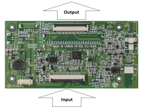
(Input): eDP (2Lane) signals with ZIF-30/40P connector.
(Output): LVDS (Single/Dual Port) with DF14-30S/ZIF-40P connector.
- 2-Lane DisplayPortTM receiver speed up to 1.62/2.7Gbps per Lane.
- Support AUX channel and HPD detection.
- Support LVDS VESA format, DE mode, Res. up to 1920×1080 via dual port.
- Support LVDS Spread-Spectrum clock to reduce EMI.
- Optional AVDD,VGH,VGL,VCOM circuit within the ZIF output connector.
- Optional Inner backlight driver.
Ordering Information:
Part Number: FR-e2Lx y a b mn
- X : Define Main Power(PWR-IN), Backlight Power (BL-VCC) and Panel Power (PNL-VDD).
X PWR-IN BL-VCC PNL-VDD 0 3.3V 5V 2.8V 1 3.3V 5V 3.3V 2 5V 12V 5V 3 5V 12V 12V - Y : The Input Connector Selection
- Input Connector (ZIF-30P).
- Input Connector (ZIF-40P).
- a : The LVDS Output Connector Selection
- DF14-30P.
- ZIF-40P/0.5mm/Down contact.
- ZIF-40P/0.5mm/Dual contact.
- b : The LVDS Output Pin Assignment Version
- A version.
- B version.
- mn : The BL and Touch Connector.

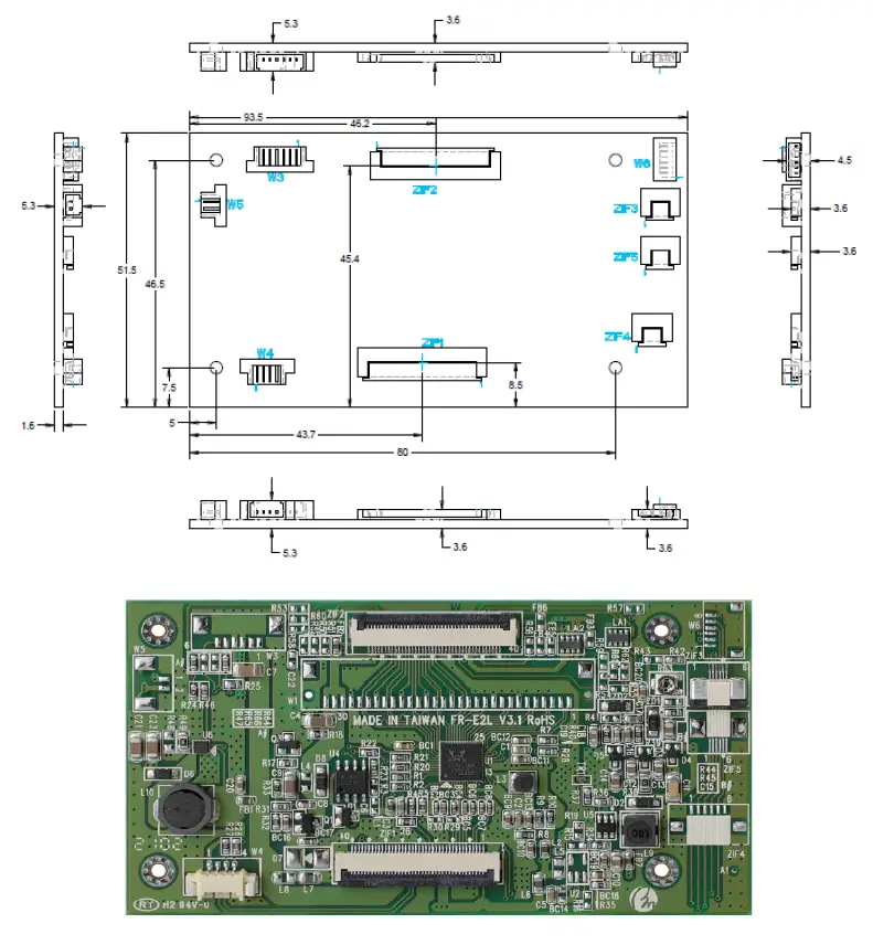
Pin Assignment
Input Interface
| eDP Input Connector(ZIF1): ZIF-30P/40P | |||
| Pin num | Description | Pin num | Description |
| Pin1 (*) | PWR-IN (3.3V/5V) | Pin2 | GND |
| Pin3 | EDP_TX1N | Pin4 | EDP_TX1P |
| Pin5 | GND | Pin6 | EDP_TX0N |
| Pin7 | EDP_TX0P | Pin8 | GND |
| Pin9 | EDPAUXP | Pin10 | EDPAUXN |
| Pin11 | GND | Pin12 (*) | PWR-IN (3.3V/5V) |
| Pin13 (*) | PWR-IN (3.3V/5V) | Pin14 (*) | PWR-IN (3.3V/5V) |
| Pin15 | GND | Pin16 | GND |
| Pin17 | HPD | Pin18 | GND |
| Pin19 | GND | Pin20 | GND |
| Pin21 | GND | Pin22 | NC |
| Pin23 | BL-PWM-In (logical 3.3V) | Pin24 | NC |
| Pin25 | NC | Pin26 (*) | BL-VCC (input) |
| Pin27 (*) | BL-VCC (input) | Pin28 (*) | BL-VCC (input) |
| Pin29 (*) | BL-VCC (input) | Pin30 | NC |
| Pin31(**) | NC | Pin32(**) | NC |
| Pin33(**) | Touch_GND | Pin34(**) | NC |
| Pin35(**) | Reserved for Touch_PWR_IN | Pin36(**) | NC |
| Pin37(**) | Reserved for Touch_SCL/(D+) | Pin38(**) | Reserved for Touch_SDA/(D-) |
| Pin39(**) | Reserved for Touch_INT(3.3V) | Pin40(**) | Reserved for Touch_RST(3.3V) |
(*). The power source of PWR-IN and BL-VCC, definition refer to Table-1. (**).These pins only available for ZIF-40P model (FR-e2Lx4Zxx).
Backlight Control Signals Output Interface
| Backlight Output Connector(W3): Wafer-6P-1.25mm | |||
| Pin num | Description | Pin num | Description |
| Pin1,2 | BL-VCC, wired to pin26,27,28,29 of the eDP input connector(ZIF1) | ||
| Pin3 | GND | Pin4 | GND |
| Pin5 | BL-EN (active high,3.3V) | Pin6 | BL-PWM-Out (3.3V) |
Touch Signals Extension Connectors
Over the touch signals extension connectors to make a connection between touch panel and HOST.
| Touch Signals Extension Connector (ZIF3/W6) Option: (ZIF3): ZIF-6P-0.5mm (W6): Wafer-6P-1.25mm | |||
| Pin num | Description | Pin num | Description |
| Pin1 | (PWR)Wired to pin35 of ZIF1 | Pin2 | (RST)Wired to pin40 of ZIF1 |
| Pin3 | (INT)Wired to pin39 of ZIF1 | Pin4(***) | (SCL/D+)Wired to pin37 of ZIF1 |
| Pin5(***) | (SDA/D-)Wired to pin38 of ZIF1 | Pin6 | GND |
The LVDS output Interface(W1)
| LVDS Output Connector(W1): DF14-30P | |||
| Pin num | Description | Pin num | Description |
| Pin1 | TXE3+ | Pin2 | TXE3- |
| Pin3 | TXEC+ | Pin4 | TXEC- |
| Pin5 | TXE2+ | Pin6 | TXE2- |
| Pin7 | GND | Pin8 | TXE1+ |
| Pin9 | TXE1- | Pin10 | GND |
| Pin11 | TXE0+ | Pin12 | TXE0- |
| Pin13 | TXO3+ | Pin14 | TXO3- |
| Pin15 | GND | Pin16 | TXOC+ |
| Pin17 | TXOC- | Pin18 | GND |
| Pin19 | TXO2+ | Pin20 | TXO2- |
| Pin21 | GND | Pin22 | TXO1+ |
| Pin23 | TXO1- | Pin24 | GND |
| Pin25 | TXO0+ | Pin26 | TXO0- |
| Pin27 | GND | Pin28 (****) | PNL-VDD |
| Pin29 (****) | PNL-VDD | Pin30 (****) | PNL-VDD |
The optional LVDS output interface(ZIF2) with pin multiplexing
(Available FR-e2Lx”4Z”xx only) To know detail about the most of pin multiplexing within ZIF2, don’t hesitate to contact your sales person, asking a help to check if ZIF2 is suitable with customer’s LCM panel interface.
| LVDS Output Connector(ZIF2): ZIF-40P/0.5mm/Down contact | |||
| Pin num | Description | Pin num | Description |
| Pin1 | Vcom/ NC | Pin2 | PNL-VDD |
| Pin3 | PNL-VDD | Pin4 | PNL-VDD/ NC |
| Pin5 | Reset/ NC | Pin6 | NC |
| Pin7 | NC | Pin8 | TX0- |
| Pin9 | TX0+ | Pin10 | GND |
| Pin11 | TX1- | Pin12 | TX1+ |
| Pin13 | GND | Pin14 | TX2- |
| Pin15 | TX2+ | Pin16 | GND |
| Pin17 | TXCLK- | Pin18 | TXCLK+ |
| Pin19 | GND | Pin20 | TX3- |
| Pin21 | TX3+ | Pin22 | GND |
| Pin23 | GND | Pin24 | GND |
| Pin25 | GND | Pin26 | NC |
| Pin27 | BL_PWM_IN/ NC | Pin28 | 68 SEL/ BL-EN/ NC |
| Pin29 | AVDD/ BL_EN/ GND/ NC | Pin30 | PNL-VDD |
| Pin31 | LED_Cathode/_Anode/NC | Pin32 | LED_Cathode/_Anode/NC |
| Pin33 | LED_Cathode/_Anode/NC | Pin34 | GND/ NC |
| Pin35 | VGL/ PULL_H/ BL_PWM/ NC | Pin36 | BL_EN/ NC |
| Pin37 | GND | Pin38 | VGH/ LED_Anode/ NC |
| Pin39 | LED_Anode/ NC | Pin40 | LED_Anode/ NC |
Inner Backlight Driver Output Interface (Option)
The (max.) driving capability of inner Backlight driver is 3.5W and only available while the BL-VCC power is DC-5V as well. The output of backlight driver is reserved on connectors W5 and ZIF1-40p.
| Backlight Output Connector(W5): Wafer-2P-1.25mm | |||
| Pin num | Description | Pin num | Description |
| Pin1 | LED_Cathode | Pin2 | LED_Anode |
Dimension: 51.5mm (w) x 93.5mm(L) x 5.3mm(H)