Zenchant Electronics ZEN-BDM10A-V2.0 Dual Mode Bluetooth Module
 Overview
 Overview
Features
- Comply with Bluetooth 5.0 specification
- Support BLE data transfer
- Support HID Profile
- Support the GATT
- Support for classic Bluetooth protocol (A2DP/AVRCP/HFP/SPP/HID)
- The 16-bit stereo audio DAC output
- 12-bit precision 1-channel stereo audio ADC with MIC amplifier circuit
- Support IIS digital audio output
- External audio input interface
- Three-way high-speed UART interface
- USB 2.0 Full Speed OTG control interface
- Support U disk, card reader, USB sound card, and other applications
- SDIO read-write SD/MMC CARDS are supported.
- The module is equipped with a 2.4g PCB antenna
Applications
- Bluetooth speakers
- Smart home
- The data transfer
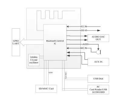
Functional Block Diagram
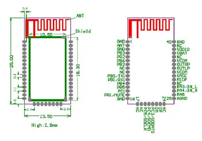
Pin Configuration
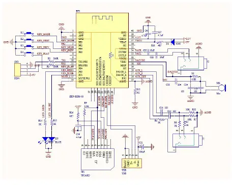
Typical application circuits
Module hardware function specifications
- PMU Characteristics
| Symbol | Parameter | Min | Typ | Max | Unit | Test Conditions |
| VBA | Voltage Input | 2.2 | 3.7 | 5.5 | V | |
| VIDEO | Voltage output | — | 3.3 | — | V | VBAT = 5V,100mA |
| VIC | ADC/DAC Voltage | — | 3.1 | — | V | VBAT = 5V,100mA |
| VIDEO | Loading current | — | — | 150 | mA | VBAT =5V |
- IO Input/Out Electrical Logical Characteristics
| IO Input Characteristics | ||||||
| Symbol | Parameter | Min | Typ | Max | Unit | Test Conditions |
| VIL | Low-Level Input Voltage | -0.3 | — | 0.3* VIDEO | V | VDDIO = 3.3V |
| VIA | High-Level Input Voltage | 0.7* VIDEO | 3.3 | — | V | VBAT = 5V,100mA |
| IO output characteristics | ||||||
| VOL | Low-Level | — | — | 0.33 | V | VDDIO = 3.3V |
| Output Voltage | ||||||
| VEOH | High-Level Output Voltage | 2.7 | — | — | V | VDDIO=3.3V |
- Internal Resistor Characteristics
| Port | General Output | High Drive | Internal Pull-Up Resistor | Internal Pull-Dow n Resistor | Comment |
| PAx PCx | 8mA | 24mA | 10K | 10K | 1. PR1 Default Out 0 2. PR2 Default Pull up 3. USBDP/DM default pull down |
| PBx | 4mA | 8mA | 10K | 10K | |
| PRx | 8mA | 10mA | 10K | 10K | |
| USBDM USBDP | 4mA | — | 1.5K | 15K |
- DAC Characteristics
| Parameter | Min | Typ | Max | Unit | Test Conditions |
| Frequency Response | 20 | — | 20K | Hz | 1KHz/0dB 10Kohm Loading With A-Weighted Filter |
| THD+N | — | -69 | — | dB | |
| S/N | — | 95 | — | dB | |
| Crosstalk | — | -80 | — | dB | |
| Output Swing | 1 | Vrms | |||
| Dynamic Range | 90 | dB | 1KHz/-60dB 10Kohm Loading With A-Weighted Filter | ||
| DAC Output Power | 11 | mW | 32-ohm Loading |
- ADC Characteristics
| Parameter | Min | Typ | Max | Unit | Test Conditions |
| Dynamic Range | 85 | dB | 1KHz/-60dB 10Kohm Loading With A-Weighted Filter | ||
| S/N | 90 | dB | 1KHz/-60dB 10Kohm Loading With A-Weighted Filter | ||
| THD+N | -72 | dB | |||
| Crosstalk | -80 | dB |
- BT Characteristics Transmitter Basic Data Rate
| Parameter | Min | Typ | Max | Unit | Test Conditions | |
| RF Transmit Power | 0 | 4 | dBm |
25℃, Power Supply Voltage=5V 2441MHz | ||
| RF Power Control Range | 20 | dB | ||||
| 20dB Bandwidth | 950 | KHz | ||||
| Adjacent Channel Transmit Power | +2MHz | -40 | dBm | |||
| -2MHz | -38 | dBm | ||||
| +3MHz | -44 | dBm | ||||
| -3MHz | -35 | dBm | ||||
- Enhanced Data Rate
| Parameter | Min | Typ | Max | Unit | Test conditions |
| Relative Power | 1.2 | dBm | ||||
| π/4 DQPSK | DEVM RMS | 6 | % | |||
| Modulation Accuracy | DVM 99% | 10 | % | 25℃, Power Supply Voltage=5V 2441MHz | ||
| DEVM Peak | 15 | % | ||||
| Adjacent | +2MHz | -40 | dBm | |||
| Channel | -2MHz | -38 | dBm | |||
| Transmit | +3MHz | -44 | dBm | |||
| Power | -3MHz | -35 | dBm | |||
- Receive Basic Data Rate
| Parameter | Min | Typ | Max | Unit | Test Conditions | |
| Sensitivity | -89 | dBm |
25℃, Power Supply Voltage=5V 2441MHz | |||
| Co-channel Interference Rejection | -13 | dB | ||||
|
Adjacent Channel Transmit Power | +1MHz | +5 | dBm | |||
| +1MHz | +2 | dBm | ||||
| +2MHz | -37 | dBm | ||||
| -2MHz | -36 | dBm | ||||
| +3MHz | -40 | dBm | ||||
| -3MHz | -35 | dBm | ||||
- Enhanced Data Rate
| Parameter | Min | Typ | Max | Unit | Test Conditions | |
| Sensitivity | -89 | dBm |
25℃, Power Supply Voltage=5V 2441MHz | |||
| Co-channel Interference Rejection | -13 | dB | ||||
|
Adjacent Channel Transmit Power | +1MHz | +5 | dBm | |||
| +1MHz | +2 | dBm | ||||
| +2MHz | -37 | dBm | ||||
| -2MHz | -36 | dBm | ||||
| +3MHz | -40 | dBm | ||||
| -3MHz | -35 | dBm | ||||
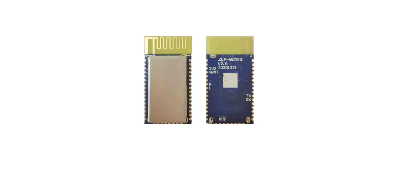
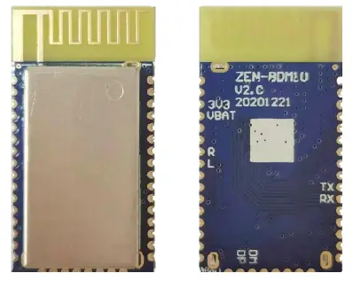
- Product options
| Model | Instructions | Photo |
|
ZEN-BDM10_V2. 0 |
Generic version | 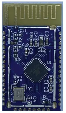 |
|
ZEN-BDM10A-V 2.0 |
With a mask version | 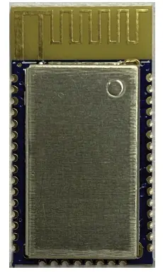 |
- Release notes
| Date | Version | Instructions |
| 2020.08.13 | V1.0 | New document |
| 2020.10.14 | V1.1 | Modify typical application circuit for USB |
| 2021.01.29 | V2.0 | The hardware version is modified to v2.0, The The antenna part is mainly modified |
FCC Statement
This device complies with part 15 of the FCC rules. Operation is subject to the following two conditions:
- this device may not cause harmful interference, and
- this device must accept any interference received, including interference that may cause undesired operation.
NOTE: The manufacturer is not responsible for any radio or TV interference caused by unauthorized modifications or changes to this equipment. Such modifications or changes could void the user’s authority to operate the equipment.
NOTE: This equipment has been tested and found to comply with the limits for a Class B digital device, pursuant to part 15 of the FCC Rules. These limits are designed to provide reasonable protection against harmful interference in a residential installation. This equipment generates uses and can radiate radio frequency energy and, if not installed and used in accordance with the instructions, may cause harmful interference to radio communications. However, there is no guarantee that interference will not occur in a particular installation. If this equipment does cause harmful interference to radio or television reception, which can be determined by turning the equipment off and on, the user is encouraged to try to correct the interference by one or more of the following measures:
- Reorient or relocate the receiving
- Increase the separation between the equipment and
- Connect the equipment into an outlet on a circuit different from that to which the receiver is connected.
- Consult the dealer or an experienced radio/TV technician for help.
This device is intended only for OEM integrators under the following conditions:
- The antenna must be installed such that 20 cm is maintained between the antenna and users.
- The transmitter module may not be co-located with any other transmitter or antenna. As long as the two conditions above are met, additional transmitter testing will not be required. However, the OEM integrator is still responsible for testing their end-product for any additional compliance requirements required for the installed
Important Note:
In the event that these conditions cannot be met (for example certain laptop configurations or co-location with another transmitter), then the Federal Communications Commission of the U.S. Government (FCC) and the Canadian Government authorizations are no longer considered valid and the FCC ID and IC ID cannot be used on the final product. In these circumstances, the OEM integrator shall be responsible for re-evaluating the end-product (including the transmitter) and obtaining a separate FCC and IC authorization in the U.S. and
Canada.
OEM Integrators – End Product Labeling Considerations:
This transmitter module is authorized only for use in device where the antenna may be installed such that 20 cm may be maintained between the antenna and users. The final end product must be labeled in a visible area with the following: “Contains, FCC ID:
2AOC9-ZENBDM10AV20. The grantee’s FCC ID can be used only when all FCC compliance requirements are met.
OEM Integrators – End Product Manual Provided to the End User:
The OEM integrator shall not provide information to the end user regarding how to install or remove this RF module in end product user manual.
The end user manual must include all required regulatory information and warnings as outlined in this document.


 Module User Manual")


