VANTEON ADRV9002 vProtean Software Defined Radio
Introduction
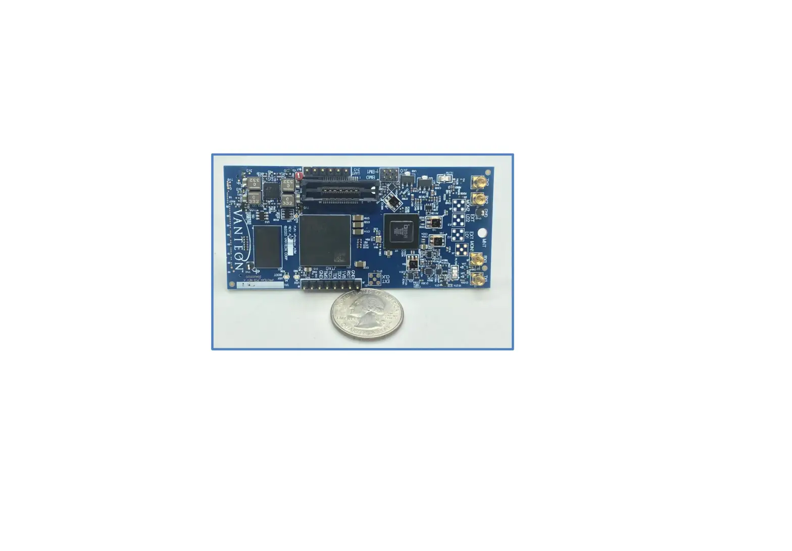
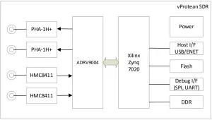
The Vanteon vProteanTM is a 2×2 MIMO software defined radio (SDR) that targets signal intelligence and multi-band processing applications. It is based on the Analog Devices ADRV9004 highly integrated wideband RF transceiver and the Xilinx Zynq-7020 All Programmable System-on-Chip (SoC). The vProtean SDR has a custom RF front end that is highly flexible, allowing its frequency range to be configured from 30 to 6000 MHz, and its instantaneous bandwidth from 12 kHz to 40 MHz.
Proper Care and Handling
All Vanteon products are thoroughly tested before shipment. The vProtean SDR is guaranteed to be functional at the time it is received by the customer. Improper use or handling of the vProtean SDR can easily cause the device to become non-functional. Listed below are some examples of actions which can prevent damage to the unit:
- Never allow metal objects to touch the circuit board while powered.
- Always properly terminate the transmit port with an antenna or 50 load.
- Always handle the board with proper anti-static methods.
- Never allow the board to directly or indirectly come into contact with any voltage spikes.
- Never allow any water, or condensing moisture, to come into contact with the boards.
- Never apply more than 0 dBm of power into any RF input.
- Always use at least 30dB attenuation if operating in a loopback configuration.
The vProtean SDR is sold for evaluation purposes and test equipment. If you choose to use your vProtean and Carrier to transmit using an antenna, it is your responsibility to make sure that you are in compliance with all laws for the country, frequency, and power levels in which the device is used. Additionally, some countries regulate reception in certain frequency bands. Again, it is the responsibility of the user to maintain compliance with all local laws and regulations.
Technical Overview
Block Diagram
High Level Specifications
| Frequency Band 1 | 30 to 6000 MHz |
| Instantaneous Bandwidth | 12 kHz to 40 MHz |
| Number of transmitters | 2 |
| Number of receivers | 2 |
| Output Transmit Power | Variable up to 19 dBm |
| Dimensions | 9.0 cm x 4.2 cm |
| Host interface | UART, USB, Ethernet, I2C and SD Card |
| Antenna connections | MMCX RF connectors |
| Power control | Wide range of output power from –20 dBm to +19 dBm |
| Flash | 512 Mb |
| DDR SDRAM | 4 Gb |
| Input Voltage | 2.0 VDC to 3.6 VDC |
| Front End Module Voltage | 3.3 VDC to 4.5 VDC |
Hardware Interfaces
Connectors
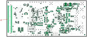
The vProtean SDR has a number of connectors that allow it to be interfaced to a host carrier board, and connectors for antennas. That table below lists all of the connectors and their associated functions. This is followed by board diagrams showing the location of each connector.
| Connector | Type | Function |
| J1 | 1×6 6 pin header | UART |
| J2 | 2×50 100 pin header | JTAG, UART, Boot Mode, Power, Reset, USB, Ethernet, SD Card, I2C, GPIO |
| J3 | Antenna | Transmit 1 |
| J4 | Antenna | Unused |
| J5 | Antenna | Receive 1 |
| J6 | 1×8 8 pin header | JTAG |
| J7 | Antenna | Transmit 2 |
| J8 | Antenna | Unused |
| J9 | Antenna | Receive 2 |
| J10 | MICTOR | Debug |
| J11 | Antenna | External Clock |
| J12 | Antenna | External LO1 |
| J13 | Antenna | External LO2 |
| SW1 | 2×3 6 pin header | Boot Mode |
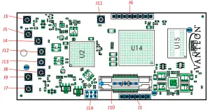
J1 Connector
The J1 connector is a 6 pin header which provides a serial console interface.
| Pin | Description |
| 1 | GND |
| 2 | Unused |
| 3 | VCC_SYS |
| 4 | FTDI_TXD_3P3V |
| 5 | FTDI_RXD_3P3V |
| 6 | Unused |
J2 Connector
The J2 connector is a 100 pin header which may be used as an interface to a host carrier board, such as the Vanteon Carrier board. The connector provides signals for several peripheral interfaces including JTAG, UART, USB, Ethernet, SD Card, I2C and GPIO. Unless otherwise noted, minimum voltage for ground (GND) is PCB ground.
| Pin ID | Mnemonic | Type | Description |
| 1, 3, 5, 7 | VCC_1P8V | Power | 1.8 V nominal to GND |
| 2, 4, 6, 8 | VCC_SYS | Power | |
| 9, 10, 11, 12 | GND | Power | PCB Ground |
| 13 | UART0_TXD_1P8V | Output | UART transmit |
| 14, 16 | VCC_3P3V | Power | 3.3 V nominal to GND |
| 15 | PS_BOOT_MODE0 | Input | Boot Mode Logic |
| 17 | PS_BOOT_MODE1 | Input | Boot Mode Logic |
| 18 | GND | Power | PCB Ground |
| 19 | PS_GPIO | Input/Output | General Purpose I/O, 1.8 V nominal |
| 20 | GND | Power | PCB Ground |
| 21 | PS_GPIO1 | Input/Output | General Purpose I/O, 1.8 V nominal |
| 22 | VCC_1P0V | Power | 1.0 V nominal to GND |
| 23 | SDCARD_CD | Input | If SD Card used, will be input. Otherwise can be used for 3.3V GPIO. |
| 24 | GND | Power | PCB Ground |
| 25 | UART0_RXD_1P8V | Input | UART Receive |
| 26 | USB_DATA2 | Input/Output | USB Data |
| 27 | USB_CTL.CLKOUT | Output | USB Clock |
| 28 | USB_DATA6 | Input/Output | USB Data |
| 29 | USB_CTL.DIR | Input | USB Control |
| 30 | USB_DATA3 | Input/Output | USB Data |
| 31 | USB_CTL.NXP | Input | USB Control |
| 32 | USB_DATA7 | Input/Output | USB Data |
| 33 | USB_CTL.STP | Input | USB Control |
| 34 | USB_DATA5 | Input/Output | USB Data |
| 35 | USB_CTL.RESET_n | Input | USB Reset |
| 36 | USB_DATA4 | Input/Output | USB Data |
| 37 | PS_SRSTn | Input | Open-drain wire-or. Drive with open- drain or switch closure to GND. |
| 38 | USB_DATA1 | Input/Output | USB Data |
| 39 | GND | Power | PCB Ground |
| 40 | USB_DATA0 | Input/Output | USB Data |
| 41 | ETH0.TX.CLK | Input | MII Clock Transmit |
| 42 | GND | Power | PCB Ground |
| 43 | ETH0.TX.D0 | Output | MII Data Transmit |
| 44 | ETH0.RESET_n | Input | MII Reset |
| 45 | ETH0.TX.D1 | Output | MII Data Transmit |
| 46 | ETH0.RX.CLK | Input | MII Clock Receive |
| 47 | ETH0.TX.D2 | Output | MII Data Transmit |
| 48 | ETH0.RX.CTRL | Input | MII Receive Enable |
| 49 | ETH0.TX.D3 | Output | MII Data Transmit |
| 50 | ETH0.RX.D1 | Input | MII Data Receive |
| 51 | ETH0.TX.CTRL | Output | MII Transmit Enable |
| 52 | ETH0.MDIO | Input/Output | MII Management Data I/O |
| 53 | GND | Power | PCB Ground |
| 54 | ETH0.RX.D3 | Input | MII Data Receive |
| 55 | J1_GPIO7 | Input/Output | General Purpose I/O, 1.8 V nominal |
| 56 | ETH0.RX.D0 | Input | MII Data Receive |
| 57 | J1_GPIO4 | Input/Output | General Purpose I/O, 1.8 V nominal |
| 58 | ETH0.RX.D2 | Input | MII Data Receive |
| 59 | J1_GPIO5 | Input/Output | General Purpose I/O, 1.8 V nominal |
| 60 | ETH0.MDC | Output | MII Management Data Clock |
| 61 | J1_GPIO0 | Input/Output | General Purpose I/O, 1.8 V nominal |
| 62 | GND | Power | PCB Ground |
| 63 | J1_GPIO2 | Input/Output | General Purpose I/O, 1.8 V nominal |
| 64 | SD_CARD.D2 | Input/Output | microSD Card Data |
| 65 | J1_GPIO3 | Input/Output | General Purpose I/O, 1.8 V nominal |
| 66 | SD_CARD.CMD | Output | microSD Card Data |
| 67 | J1_GPIO6 | Input/Output | General Purpose I/O, 1.8 V nominal |
| 68 | SD_CARD.D1 | Input/Output | microSD Card Data |
| 69 | J1_GPIO1 | Input/Output | General Purpose I/O, 1.8 V nominal |
| 70 | SD_CARD.D3 | Input/Output | microSD Card Data |
| 71 | GND | Power | PCB Ground |
| 72 | SD_CARD.D0 | Input/Output | microSD Card Data |
| 73 | J_TMS | Input | JTAG Test Mode Select |
| 74 | SD_CARD.CLK | Output | microSD Card Clock |
| 75 | J_TDO | Output | JTAG Test Data Output |
| 76 | GND | Power | PCB Ground |
| 77 | J_TDI | Input | JTAG Test Data Input |
| 78 | I2C_SDA | Input/Output | I2C Serial Data |
| 79 | J_TCK | Input | JTAG Test Clock |
| 80 | I2C_SCL | Output | I2C Serial Clock |
| 81, 82 | GND | Power | PCB Ground |
| 83 | SPARE_PAIRS.0._N | Input/Output | Differential I/O Pairs, 2.5 V nominal |
| 84 | SPARE_PAIRS.3._P | Input/Output | Differential I/O Pairs, 2.5 V nominal |
| 85 | SPARE_PAIRS.0._P | Input/Output | Differential I/O Pairs, 2.5 V nominal |
| 86 | SPARE_PAIRS.3._N | Input/Output | Differential I/O Pairs, 2.5 V nominal |
| 87, 88 | GND | Power | PCB Ground |
| 89 | SPARE_PAIRS.1._P | Input/Output | Differential I/O Pairs, 2.5 V nominal |
| 90 | SPARE_PAIRS.2._P | Input/Output | Differential I/O Pairs, 2.5 V nominal |
| 91 | SPARE_PAIRS.1._N | Input/Output | Differential I/O Pairs, 2.5 V nominal |
| 92 | SPARE_PAIRS.2._N | Input/Output | Differential I/O Pairs, 2.5 V nominal |
| 93, 94, 95, 96, 97, 98, 99, 100 | GND | Power | PCB Ground |
J6 Connector
The J6 connector is a 8 pin header which provides a JTAG interface.
| Pin | Description |
| 1 | GND |
| 2 | JTAG_TMS |
| 3 | JTAG_TCK |
| 4 | JTAG_TDI |
| 5 | JTAG_TDO |
| 6 | VCC_1P8V |
| 7 | PS_SRSTn |
| 8 | GND |
J14 Connector
The J14 connector is a 6 pin header that defines the boot mode for vProtean
| Pin | Description |
| 1 | GND |
| 2 | JTAG_TMS |
| 3 | JTAG_TCK |
| 4 | JTAG_TDI |
| 5 | JTAG_TDO |
| 6 | VCC_1P8V |
| 7 | PS_SRSTn |
| 8 | GND |
The boot mode settings are defined by pins 3 and 4.
| Mode | PS_BOOT_MODE0 | PS_BOOT_MODE1 |
| JTAG | 0 | 0 |
| QSPI | 0 | 1 |
| SD Card | 1 | 1 |
The boot mode jumpers are provided on the vProtean SDR and the Carrier board. The vProtean SDR boot mode jumpers should only be used when the vProtean SDR is used without the Vanteon Carrier board. Otherwise, the Carrier board vProtean jumpers should be used.
LEDs
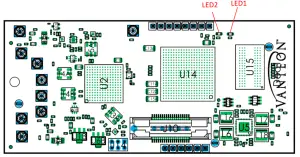
The vProtean software defined radio has two (2) LEDs, whose function is described in the table below.
This is followed by a board diagram showing the location of each LED.
| LED1 | Blue | On when Zynq 7020 programmable logic has been programmed |
| LED2 | Green | Software control |
User Console
If the vProtean SDR was purchased as part of an evaluation kit, it is preloaded with a menu-based application that allows a user to perform transmit and receive functions. This section explains how to use the vProtean SDR evaluation application.
UART
The simplest method to access the preloaded test application on the vProtean SDR is to mount it to a the Vanteon Carrier board. The Carrier board provides a serial console interface via the Type-C USB connector. Connect the vProtean Carrier Board to a PC using the appropriate USB cable. Use a terminal emulator program on the PC to open a terminal session using the virtual COM port associated with the vProtean Carrier Board. The serial port parameters are: 115200 baud, 8 bits, no parity, 1 stop bit, no handshaking.
The vProtean software defined radio has a hierarchical menu structure that allows you to configure the radio and to transmit and receive test waveforms. The main menu consists of the following status and commands:
| Item | Name | Function |
| – | TX RX Sample Rate | Display of the pre-configured sample rate (not user changeable) |
| – | FPGA Temperature | Display of the FPGA temperature |
| – | ADRV Temperature | Display of the RF IC temperature |
| – | RX1 RSSI | Display of RX1 RSSI |
| – | RX2 RSSI | Display of RX2 RSSI |
| 1 | TX1 RX1 Settings | Configure TX1 and RX1 |
| 2 | TX2 RX2 Settings | Configure TX2 and RX2 |
| 3 | Capture RX | Initiate RX capture according to RX capture settings |
| 4 | RX Capture Waveform Settings | Configure the RX capture parameters |
| 5 | Recalibrate System | Force a transceiver recalibration |
TX1/RX1 and TX2/RX2 Settings Menu
There are two submenus for configuring the TX1/RX1 and TX2/RX2 pairs. This section covers both submenus, and refers to TX1 and TX2 as a generic TX_, and RX1 and RX2 as a generic RX_.
| Item | Name | Function |
| 1 | TX_/RX_ Frequency | Set the TX_/RX_ frequency (30 MHz to 6000 MHz) |
| 2 | Toggle TX_ | Toggles transmit for TX_ on/off |
| 3 | TX_ Waveform Select | Go to TX_ waveform select menu |
| 4 | Digital Attenuation (dB) | Attenuation that is applied digitally to the transmit waveform (0 to 100 dB) |
| 5 | TX_ Front End Atten (dB) | Sets the attenuation in the ADRV9004 (0 to 41.5 dB), value can only be changed when TX is enabled |
| 6 | TX_ BOOST | Adds an additional 3 dB to the transmit |
| 7 | Toggle RX_ | Toggles receive for RX_ on/off |
Note: The vProtean SDR may require external cooling, should both transmit channels be used continuously. The FPGA and ADRV temperatures displayed on the main menu should be monitored by the user, and external cooling (i.e. directed fan) should be applied as needed.
TX1 and TX2 Waveform Select Menu
The TX Waveform Select Menu configures the waveform that is transmitted when the TX is toggled on. When the transmit is enabled, the selected waveform is transmitted repeatedly.
| Item | Name | Function |
| – | Current Waveform | Display the current selected waveform |
| 1 | Zeros | Fills transmit buffer with zero waveform |
| 2 | CW | Single tone at carrier frequency |
| 3 | USB Tone, Offset=FS/32 | Upper side band waveform, FS=sample rate |
| 4 | Dual Tone, Offset=FS/32+FS/8 | Dual tone waveform, FS=sample rate |
| 5 | File | Go to file select menu to load waveform file from SD card |
TX1 and TX2 File Select Menu
The File Menu allows the user to select a user defined file that specifies the transmit waveform.
The file must exist on the SD card to be listed in this menu. The format of the filename must have a “.iq” extension to show up in the file list.
The format of a transmit waveform is a .CSV file with one sample (IQ p air) per line with I and Q values separated by a comma.
For Version 1.x Software
The TX waveform file must contain between a minimum of 256 samples and a maximum of 2,097,150 samples, inclusive.
For Version 2.x Software
The TX waveform file must contain between a minimum of 512 samples and a maximum of 4,194,304 samples, inclusive. The number of samples should be a multiple of 512. If the number of samples is not a multiple of 512, the TX waveform will be zero padded to the next multiple of 512.
Note: The vProtean SDR and Carrier board should be powered down whenever mounting or removing the SD card.
RX Waveform Capture Settings Menu
The RX Waveform Capture Settings Menu allows the user to set the number of samples captured and the file to which the samples are saved. It also allows the user to configure which RX channel will be captured.
The format of a captured waveform is a .CSV file with one sample (IQ pair) per line with I and Q values separated by a comma.
If the captured waveform filename has an “.iq” extension it will show up in the TX waveform list if the capture was successful.
For Version 1.x Software
The number of RX samples to capture must be between a minimum of 256 samples and a maximum of 2,097,150 samples, inclusive.
For Version 2.x Software
The number of RX samples to capture must be a multiple of 512. If it is not a multiple of 512 the capture will fail.
| Item | Name | Function |
| 1 | Filename | The name of the file to save the RX samples to. The filename can be up to 9 characters. The filename extension can be up to 2 characters. It is recommended that the filename extension be “.iq” |
| 2 | Samples | The number of samples to capture. |
| 3 | RX Channel [1,2] | Configure which RX channel the capture should be performed on. |
Customer Support
If you experience difficulty after reading the manual and/or using the product, please feel free to contact [email protected] for additional assistance.
Vanteon offers contract engineering services and can assist you in implementing the vProtean SDR into your system.
Terms and Conditions of Sale
All sales of product are subject to the terms and conditions described in “Vanteon Corporation – Terms and Conditions of Product Sales”. Unless explicitly agreed to in writing, Vanteon rejects all modifications to these standard terms and conditions.
One Year Warranty
Vanteon Corporation provides a One-Year Limited Warranty for all products sold. Should this product, in Vanteon Corporation’s opinion, fail to be in good working order during the warranty period, Vanteon Corporation will, at its option, repair or replace this product at no charge, provid
ed that the product has
not been subject to abuse, misuse, accident or unauthorized modification or repair.Products returned to Vanteon must be pre-authorized by Vanteon and sent prepaid, insured, and packaged for safe shipment. Vanteon will return this product by prepaid ground shipment service.
Should the product prove to be irreparable, Vanteon reserves the right to substitute an equivalent product if available.
See accompanying “Vanteon Corporation – Terms and Conditions of Product Sales” for additional information regarding this warranty.
The above warranty is the only warranty authorized by Vanteon for this product. Under no circumstances will Vanteon be liable in any way for any damages, including any lost profits, business revenue, special, indirect, incidental, exemplary, punitive, or consequential damages arising out of the use of, or inability to use such product.
Copyright Notice
he information contained in this document is subject to change without notice. Vanteon Corporation shall not be liable for errors contained herein or for incidental or consequential damages in connection with the furnishing, performance, or use of this material. This document contains proprietary information that is protected by copyright. All rights are reserved. No part of this document may be photocopied, reproduced, or translated to another language without the prior written consent of Vanteon Corporation.
Copyright © 2020 by Vanteon Corporation.
Trademark Acknowledgement
Vanteon Corporation acknowledges all trademarks, registered trademarks and/or copyrights referred to in this document as the property of their respective owners. Not listing all possible trademarks or copyright acknowledgements does not constitute a lack of acknowledgement to the rightful owners of the trademarks and copyrights mentioned in this document.