
CIMCON Lighting CIMX1PRO V3 RF Module

No part of this document may be reproduced or transmitted in any form or by any means, electronic or mechanical, for any purpose, without the express written permission of CIMCON Lighting, Inc. Information in this document is subject to change without notice. CIMCON Lighting, Inc. may have patents or pending patent applications, trademarks, copyrights, or other intellectual property rights covering subject matter in this document. The furnishing of this document does not give you license to these patents, trademarks, copyrights, or other intellectual property except as expressly provided in any written license agreement from CIMCON Lighting, Inc.
© 2013 CIMCON Lighting,
Inc. All rights reserved.
GETTING STARTED
Overview
This manual describes the key features, pin out, recommended operating conditions, working of RF module and operating instructions to test the module for FCC.
CIMCON RF modules are designed to operate within the ZigBee protocol and support the unique needs of low-cost, low-power wireless sensor networks. The modules require minimal power and provide reliable delivery of data between remote devices. The modules operate within the ISM 2.4 GHz frequency band work on ZigBee protocol.
Key Features
The key features of RF modules are as follows:
- Operates from wide 2.1VDC to 3.6VDC
- Maximum transmit current is 150MA (Typical at 3.3V)
- Maximum Receive current is 38mA
- Maximum transmit power is +20 DBM
- Receiver Sensitivity of -104dBm
- Various serial interfaces like UART, SPI (master/ slave), and TWI
- Six external ADC sources with 14-bit resolution
- Urban range of ~85m
- Line of sight range of ~1750m
- Network Type: Self-forming mesh network
- Network Fault Tolerance: Self-healing mesh
- Data Protection: 256-bit AES encrypt
- Hardware: IEEE 802.15.4-2003 CS MA-CA algorithm3
- Operational channel: Channel 11 to 25
- 2.4GHz Zigbee radio produces an O-QPSK-modulated signal using the analog front end and digital baseband.
FCC Warnings and Labeling
Warning:
This device is intended only for OEM integrator under the following conditions:
- The antenna must be installed such that 20 cm is maintained between the antenna and users, and
- The transmitter module may not be co-located with any other transmitter or antenna,
- For all products market in US, OEM has to limit the operation channels in CH11 to CH25 for 2.4G band by supplied firmware programming tool. OEM shall not supply any tool or info to the end-user regarding to Regulatory Domain change.
As long as the three conditions above are met, further transmitter testing will not be required. However, the OEM integrator is still responsible for testing their end-product for any additional compliance requirements required with this module installed.
Important Note:
In the event that these conditions cannot be met (for example certain laptop configurations or co-location with another transmitter), then the FCC authorization is no longer considered valid and the FCC ID cannot be used on the final product. In these circumstances, the OEM integrator will be responsible for re-evaluating the end product (including the transmitter) and obtaining a separate FCC authorization.
End Product Labeling
This transmitter module is authorized only for use in device where the antenna may be installed such that 20 cm may be maintained between the antenna and users. The final end product must be labeled in a visible area with the following: Contains FCC ID: S3Z-CIM35X2.
Manual Information to the End User
The OEM integrator has to be aware not to provide information to the end user regarding how to install or remove this RF module in the user’s manual of the end product which integrates this module. The end user manual shall include all required regulatory information/warning as show in this manual.
This information is confidential and proprietary to CLI and is to be used only for the purpose for which it is provided. Reproduction by any means, electronic or mechanical, and distribution to third parties without express written permission from CLI is not permitted.
Zigbee MODULE PIN-OUT
Following is the pin out of CIMCON RF module with description of each pin
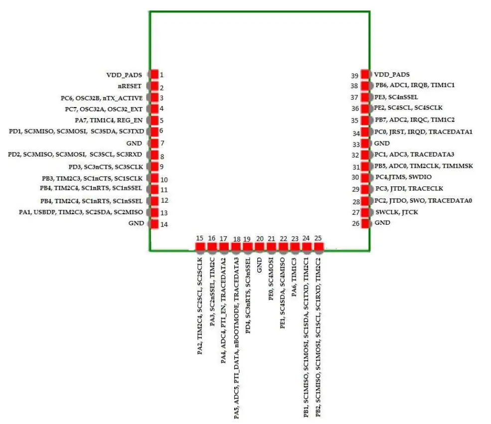
| PIN | SIGNAL | DIRECTION | DESCRIPTION |
| 1 | 3.3V | Power | Used to power the CIMCON RF module. |
| 2 | nReset | I | Active Low chip reset (Internal pull up) |
| 3 | PC6 | I/O | Digital I/O |
| OSC32B | I/O | 32.768 KHZ CRYSTAL OSCILLATOR | |
| nTX_ACTIVE | O | Inverted TX_ACTIVE signal | |
| 4 | PC7 | I/O | Digital I/O |
| OSC32A | I/O | 32.768 KHZ CRYSTAL OSCILLATOR | |
| OSC32_EXT | I | Digital 32.768 kHz clock input source | |
| 5 | PA7 | I/O | Digital I/O |
| TIM1C4 | O | Timer 1 Channel 4 output | |
| TIM1C4 | I | Timer 1 Channel 4 input | |
| REG_EN | O | External regulator open drain output | |
| 6 | PD1 | I/O | Digital I/O |
| SC3MISO | I | SPI slave data out of Serial Controller 3 | |
| SC3MOSI | O | SPI master data out of Serial Controller 3 | |
| SC3SDA | I/O | TWI data of Serial Controller 3 | |
| SC3TXD | O | UART transmit data of Serial Controller 3 | |
| 7 | GND | Power | Ground pin of RF module. |
| 8 | PD2 | I/O | Digital I/O |
| SC3MISO | I | SPI master data in of Serial Controller 3 | |
| SC3MOSI | O | SPI slave data in of Serial Controller 3 | |
| SC3SCL | I/O | TWI clock of Serial Controller 3 | |
| SC3RXD | I | UART receive data of Serial Controller 3 | |
| 9 | PD3 | I/O | Digital I/O |
| SC3nCTS | I | UART CTS handshake of Serial Controller 3 | |
| SC3SCLK | O | SPI master clock of Serial Controller 3 | |
| SC3SCLK | I | SPI slave clock of Serial Controller 3 | |
| 10 | PB3 | I/O | Digital I/O |
| TIM2C3 | O | Timer 2 channel 3 output | |
| TIM2C3 | I | Timer 2 channel 3 input | |
| SC1nCTS | I | UART CTS handshake of Serial Controller 1 | |
| SC1SCLK | O | SPI master clock of Serial Controller 1 | |
| SC1SCLK | I | SPI slave clock of Serial Controller 1 | |
| 11 | PB4 | I/O | Digital I/O |
| TIM2C4 | O | Timer 2 channel 4 output | |
| TIM2C4 | I | Timer 2 channel 4 input | |
| SC1NRTS | O | UART RTS handshake of Serial Controller 1 | |
| SC1NSSEL | I | SPI slave select of Serial Controller 1 | |
| 12 | PA0 | I/O | Digital I/O |
| TIM2C1 | O | Timer 2 channel 1 output | |
| TIM2C1 | I | Timer 2 channel 1 input | |
| SC2MOSI | O | SPI master data out of Serial Controller 2 | |
| SC2MOSI | I | SPI slave data in of Serial Controller 2 | |
| 13 | PA1 | I/O | Digital I/O |
| TIM2C3 | O | Timer 2 channel 3 output | |
| TIM2C3 | I | Timer 2 channel 3 input | |
| SC2SDA | I/O | TWI data of Serial Controller 2 | |
| SC2MISO | O | SPI slave data out of Serial Controller 2 | |
| SC2MISO | I | SPI master data in of Serial Controller 2 | |
| 14 | GND | Power | Ground pin of RF module. |
|
15 | PA2 | I/O | Digital I/O |
| TIM2C4 | O | Timer 2 channel 4 output | |
| TIM2C4 | I | Timer 2 channel 4 input Disable remap with TIM2_OR[7] | |
| SC2SCL | I/O | TWI clock of Serial Controller 2 | |
| SC2SCLK | O | SPI master clock of Serial Controller 2 | |
| SC2SCLK | I | SPI slave clock of Serial Controller 2 | |
| 16 | PA3 | I/O | Digital I/O |
| SC2nSSEL | I | SPI slave select of Serial Controller 2 | |
| TIM2C2 | O | Timer 2 channel 2 output | |
| TIM2C2 | I | Timer 2 channel 2 input | |
| 17 | PA4 | I/O | Digital I/O |
| ADC4 | Analog | ADC Input 4 | |
| PTI_EN | O | Frame signal of Packet Trace Interface (PTI) | |
| TRACEDATA2 | O | Synchronous CPU trace data bit 2 | |
| 18 | PA5 | I/O | Digital I/O |
| ADC5 | Analog | ADC Input 5 | |
| PTI_DATA | O | Data signal of Packet Trace Interface (PTI) | |
| nBOOTMODE | I | Embedded serial bootloader activation out of reset | |
| TRACEDATA3 | O | Synchronous CPU trace data bit 3 | |
| 19 | PD4 | I/O | Digital I/O |
| SC3nRTS | O | UART RTS handshake of Serial Controller 3 | |
| SC3nSSEL | I | SPI slave select of Serial Controller 3 | |
| 20 | GND | Power | Ground pin of RF module. |
| 21 | PE0 | I/O | Digital I/O |
| SC4MOSI | O | SPI master data out of Serial Controller 4 | |
| SC4MOSI | I | SPI slave data in of Serial Controller 4 | |
| 22 | PE1 | I/O | Digital I/O |
| SC4SDA | I/O | TWI data of Serial Controller 4 | |
| SC4MISO | O | SPI slave data out of Serial Controller 4 | |
| SC4MISO | I | SPI master data in of Serial Controller 4 | |
| 23 | PA6 | I/O | Digital I/O |
| TIM1C3 | O | Timer 1 channel 3 output | |
| TIM1C3 | I | Timer 1 channel 3 input | |
| 24 | PB1 | I/O | Digital I/O |
| SC1MISO | O | SPI slave data out of Serial Controller 1 | |
| SC1MOSI | O | SPI master data out of Serial Controller 1 | |
| SC1SDA | I/O | TWI data of Serial Controller 1 | |
| SC1TXD | O | UART transmit data of Serial Controller 1 | |
| TIM2C1 | O | Timer 2 channel 1 output | |
| TIM2C1 | I | Timer 2 channel 1 input | |
| 25 | PB2 | I/O | Digital I/O |
| SC1MISO | I | SPI master data in of Serial Controller 1 | |
| SC1MOSI | I | SPI slave data in of Serial Controller 1 | |
| SC1SCL | I/O | TWI clock of Serial Controller 1 | |
| SC1RXD | I | UART receive data of Serial Controller 1 | |
| TIM2C2 | O | Timer 2 channel 2 output | |
| TIM2C2 | I | Timer 2 channel 2 input | |
| 26 | GND | Power | Ground pin of RF module. |
| 27 | SWCLK | I/O | Serial Wire clock input/output with debugger |
| JTCK | I | JTAG clock input from debugger | |
| 28 | PC2 | I/O | Digital I/O |
| JTDO | O | JTAG data out to debugger | |
| SWO | O | Serial Wire Output asynchronous trace output to debugger | |
| TRACEDATA0 | O | Synchronous CPU trace data bit 3 | |
| 29 | PC3 | I/O | Digital I/O |
| JTDI | I | JTAG data in from debugger | |
| TRACECLK | O | Synchronous CPU trace clock | |
| 30 | PC4 | I/O | Digital I/O |
| JTMS | I | JTAG mode select from debugger | |
| SWDIO | I/O | Serial Wire bidirectional data to/from debugger | |
| 31 | PB5 | I/O | Digital I/O |
| ADC0 | Analog | ADC Input 0 | |
| TIM2CLK | I | Timer 2 external clock input | |
| TIM1MSK | I | Timer 1 external clock mask input | |
| 32 | PC1 | I/O | Digital I/O |
| ADC3 | Analog | ADC Input 3 | |
| TRACEDATA3 | O | Synchronous CPU trace data bit 0 | |
| 33 | GND | Power | Ground pin of RF module. |
| 34 | PC0 | I/O | Digital I/O |
| JRST | I | JTAG reset input from debugger | |
| IRQD | I | Default external interrupt source D | |
| TRACEDATA1 | O | Synchronous CPU trace data bit 1 | |
| 35 | PB7 | I/O | Digital I/O |
| ADC2 | Analog | ADC Input 2 | |
| IRQC | I | Default external interrupt source C | |
| TIM1C2 | O | Timer 1 channel 2 output | |
| TIM1C2 | I | Timer 1 channel 2 input | |
| 36 | PE2 | I/O | TWI clock of Serial Controller 4 |
| SC4SCL | I/O | TWI clock of Serial Controller 4 | |
| SC4SCLK | O | SPI master clock of Serial Controller 4 | |
| SC4SCLK | I | SPI slave clock of Serial Controller 4 | |
| 37 | PE3 | I/O | Digital I/O |
| SC4nSSEL | I | SPI slave select of Serial Controller 4 | |
| 38 | PB6 | I/O | Digital I/O |
| ADC1 | Analog | ADC Input 1 | |
| IRQB | I | External interrupt source B | |
| TIM1C1 | O | Timer 1 channel 1 output | |
| TIM1C1 | I | Timer 1 channel 1 input | |
| 39 | 3.3V | Power | Used to power the CIMCON RF module. |
CONFIGURATIONINFORMATION
A.Absolute Maximum Ratings of RF Module
The following table provides maximum ratings of RF Module:
| Sr. No. | Parameter | Symbol | Absolute Maximum ratings | Unit |
| 1 | Supply Voltage | Vcc | -0.3 to +3.6 | VDC |
| 2 | Voltage on any GPIO including nReset and JCLK | VIN | -0.3 to Vcc+0.3 | VDC |
| 3 | Voltage on any GPIO [PA4, PA5, PB5, PB6, PB7, PC1] when used as input to ADC | VIN | -0.3 to +2.0 | VDC |
| 4 | Storage Temperature Range | Tstg | -40 to +105 | °C |
| 5 | Operating Temperature Range | Top | -40 to +85 | °C |
| 6 | ESD on any pin (HBM) | Vhbm | +/-2 | KV |
| 7 | ESD on RF port (CDM) | Vcdm | +/-225 | V |
| 8 | Moisture Sensitivity Level (MSL) | MSL3 | ||
| 9 | Reflow Temperature | Treflow | Refer in next pages |
B. Recommended Operating Conditions
| Sr. No | Parameter | Symbol | Recommended Operating Conditions | Unit |
| 1 | Supply Voltage | Vcc | 2.1 to 3.6 | VDC |
| 2 | Operating frequency | Fin | 2405 to 2475 | MHz |
| 3 | Operating Temperature | Top | -40 to +85 | °C |
C. DC Electrical Characteristics
| Parameter | Test Conditions | Min. | Typical | Max | Unit |
| Voltage supply | 2.1 | 3.6 | VDC | ||
| Low Schmitt switching threshold | VSWIL Schmitt input threshold going from high to low | 0.42 x VDD_PADS | – | 0.50 x VDD_PADS | |
| High Schmitt switching threshold | VSWIH Schmitt input threshold going from low to high | 0.62 x VDD_PADS | – | 0.80 x VDD_PADS | V |
| Input current for logic 0 | IIL | – | – | -0.5 | uA |
| Input current for logic 1 | IIH | – | – | +0.5 | uA |
| Input pull-up resistor value | RIPU | 24 | 29 | 34 | kΩ |
| Input pull-down resistor value | RIPD | 24 | 29 | 34 | kΩ |
| Output voltage for logic 0 | VOL (IOL = 4 mA for standard pads, 8 mA for high current pads) | 0 | 0.18 x VDD_PADS | V | |
| Output voltage for logic 1 | VOH (IOH = 4 mA for standard pads, 8 mA for high current pads) | 0.82 x VDD_PADS | VDD_PADS | V | |
| Output source current (standard current pad) | IOHS | 4 | mA | ||
| Output sink current (standard current pad) | IOLS | 4 | mA | ||
| Output source current high current pad: PA6, PA7, PB6, PB7, PC0 | IOHH | 8 | mA | ||
| Output sink current high current pad: PA6, PA7, PB6, PB7, PC0 | IOLH | 8 | mA | ||
| Total output current (for I/O Pads) | IOH + IOL | 40 | mA |
D. Power Settings for Regulatory Compliance
Because of the high gain of the frontend module output power of up to 24DBM can be achieved When the antenna gain is included then the output power of the EM3597 transceivers needs to be reduced for regulatory compliance. The following tables list the maximum permitted power setting for the different antenna types listed. This is the power out of the EM3597 chip, and the power delivered to the antenna will be higher by the gain of the PA.
settxpower P (set the channel power)
UFL Antenna Unit
- Channel 11 TO Channel 24: P = -5 [dBm]
- Channel 25: P = -10 [dBm]
Fixed Antenna Unit
- Channel 11 to Channel 24: P = -3 [dBm]
- Channel 25: P = -10 [dBm]
BOARD LAYOUT
CIMCON RF modules do not have any specific sensitivity to nearby processors, crystal or other PCB components. Other than mechanical considerations, no special PCB placement is required for integrating CIMCON RF radios. In general, Power and GND traces should be thicker than signal traces and be able to comfortably support the maximum currents.
The radios are also designed to be self-sufficient and work with wire whip and external antennas without the need for additional ground planes on the host PCB. However, considerations should be taken on the choice of antenna and antenna location. Metal objects that are near an antenna cause reflections and may reduce the ability for an antenna to efficiently radiate. Using an integral antenna (like a wire whip antenna) in an enclosed metal box will greatly reduce the range of a radio. For this type of application an external antenna would be a better choice. External antennas should be positioned away from metal objects as much as possible. Metal objects next to the antenna or between transmitting and receiving antennas can often block or reduce the transmission distance. Some objects that are often overlooked are metal poles, metal studs or beams in structures, concrete (it is usually reinforced with metal rods), metal enclosures, vehicles, elevators, ventilation ducts, refrigerators and microwave ovens.
The Wire Whip Antenna should be straight and perpendicular to the ground plane and/or chassis. It should reside above or away from any metal objects like batteries, tall electrolytic capacitors or metal enclosures. If the antenna is bent to fit into a tight space, it should be bent so that as much of the antenna as possible is away from metal. Caution should be used when bending the antenna, since this will weaken the solder joint where the antenna connects to the module. Antenna elements radiate perpendicular to the direction they point. Thus a vertical antenna emits across the horizon.
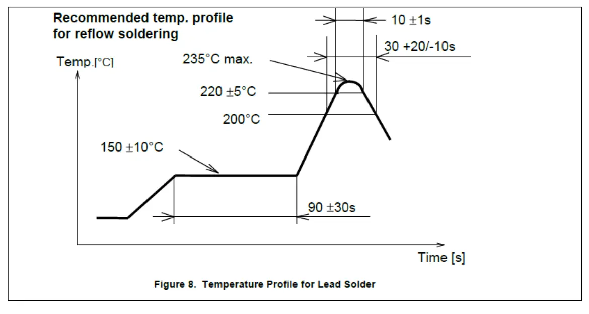
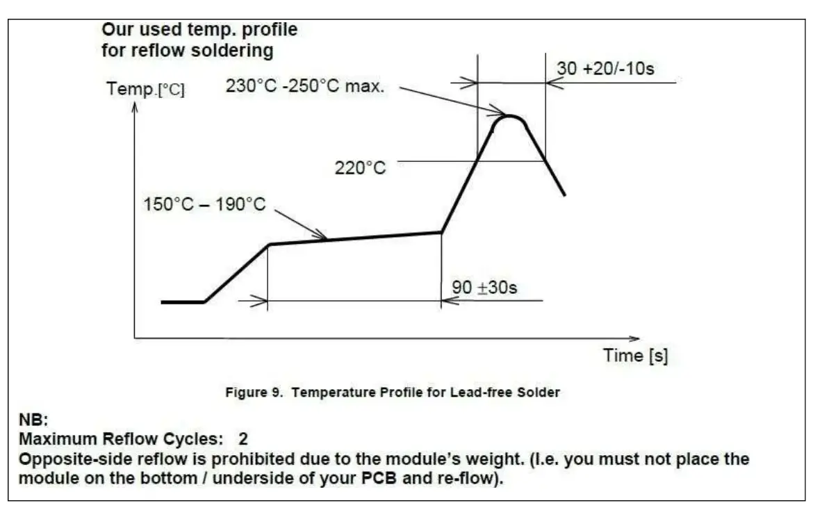
SOLDERING TEMPERATURE PROFILE
Leaded Process
Lead Free Process
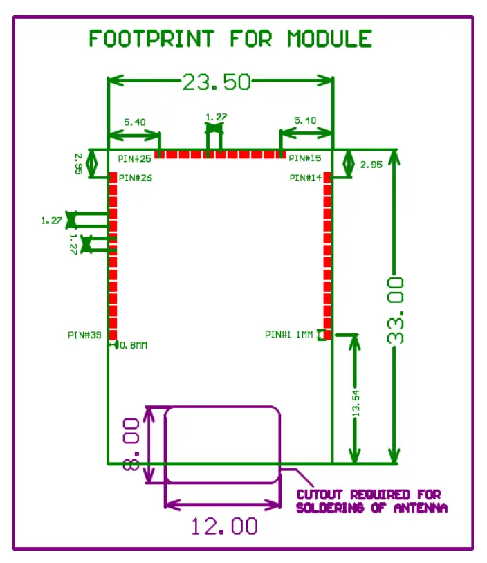
MECHANICAL DIMENSIONS OF THE SMT MODULES
Dimensions
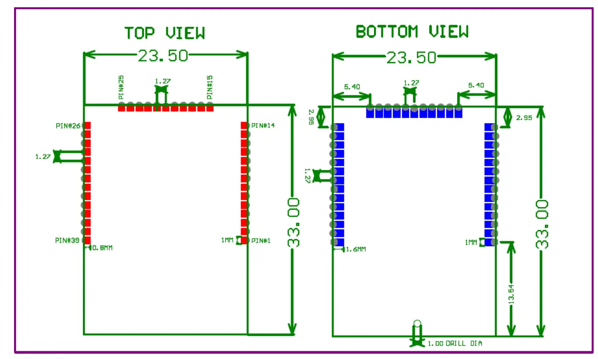
FOOTPRINT of the Module
CIMCON Lighting, Inc.
200 Summit Drive,
Suite 500, South
Tower, Burlington,
United States
www.cimconlighting.com


