ATMEL ATtiny11 8-bit Microcontroller with 1K Byte Flash
Features
- Utilizes the AVR® RISC Architecture
- High-performance and Low-power 8-bit RISC Architecture
- 90 Powerful Instructions – Most Single Clock Cycle Execution
- 32 x 8 General Purpose Working Registers
- Up to 8 MIPS Throughput at 8 MHz
Nonvolatile Program and Data Memory
- 1K Byte of Flash Program Memory
- In-System Programmable (ATtiny12)
- Endurance: 1,000 Write/Erase Cycles (ATtiny11/12)
- 64 Bytes of In-System Programmable EEPROM Data Memory for ATtiny12
- Endurance: 100,000 Write/Erase Cycles
- Programming Lock for Flash Program and EEPROM Data Security
Peripheral Features
- Interrupt and Wake-up on Pin Change
- One 8-bit Timer/Counter with Separate Prescaler
- On-chip Analog Comparator
- Programmable Watchdog Timer with On-chip Oscillator
Special Microcontroller Features
- Low-power Idle and Power-down Modes
- External and Internal Interrupt Sources
- In-System Programmable via SPI Port (ATtiny12)
- Enhanced Power-on Reset Circuit (ATtiny12)
- Internal Calibrated RC Oscillator (ATtiny12)
Specification
- Low-power, High-speed CMOS Process Technology
- Fully Static Operation
Power Consumption at 4 MHz, 3V, 25°C
- Active: 2.2 mA
- Idle Mode: 0.5 mA
- Power-down Mode: <1 μA
Packages
- 8-pin PDIP and SOIC
Operating Voltages
- 1.8 – 5.5V for ATtiny12V-1
- 2.7 – 5.5V for ATtiny11L-2 and ATtiny12L-4
- 4.0 – 5.5V for ATtiny11-6 and ATtiny12-8
Speed Grades
- 0 – 1.2 MHz (ATtiny12V-1)
- 0 – 2 MHz (ATtiny11L-2)
- 0 – 4 MHz (ATtiny12L-4)
- 0 – 6 MHz (ATtiny11-6)
- 0 – 8 MHz (ATtiny12-8)
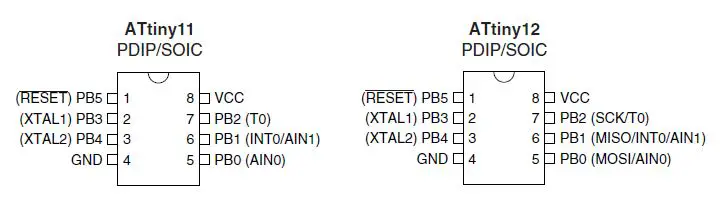
Pin Configuration
Overview
The ATtiny11/12 is a low-power CMOS 8-bit microcontroller based on the AVR RISC architecture. By executing powerful instructions in a single clock cycle, the ATtiny11/12 achieves throughputs approaching 1 MIPS per MHz, allowing the system designer to optimize power consumption versus processing speed. The AVR core combines a rich instruction set with 32 general-purpose working registers. All the 32 registers are directly connected to the Arithmetic Logic Unit (ALU), allowing two independent registers to be accessed in one single instruction executed in one clock cycle. The resulting architecture is more code efficient while achieving throughputs up to ten times faster than conventional CISC microcontrollers.
Table 1. Parts Description
| Device | Flash | EEPROM | Register | Voltage Range | Frequency |
| ATtiny11L | 1K | – | 32 | 2.7 – 5.5V | 0-2 MHz |
| ATtiny11 | 1K | – | 32 | 4.0 – 5.5V | 0-6 MHz |
| ATtiny12V | 1K | 64 B | 32 | 1.8 – 5.5V | 0-1.2 MHz |
| ATtiny12L | 1K | 64 B | 32 | 2.7 – 5.5V | 0-4 MHz |
| ATtiny12 | 1K | 64 B | 32 | 4.0 – 5.5V | 0-8 MHz |
The ATtiny11/12 AVR is supported with a full suite of program and system development tools including: macro assemblers, program debugger/simulators, in-circuit emulators,
and evaluation kits.
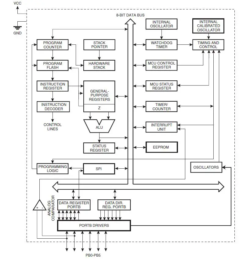
ATtiny11 Block Diagram
See Figure 1 on page 3. The ATtiny11 provides the following features: 1K bytes of Flash, up to five general-purpose I/O lines, one input line, 32 general-purpose working registers, an 8-bit timer/counter, internal and external interrupts, programmable Watchdog Timer with internal oscillator, and two software-selectable power-saving modes. The Idle Mode stops the CPU while allowing the timer/counters and interrupt system to continue functioning. The Power-down Mode saves the register contents but freezes the oscillator, disabling all other chip functions until the next interrupt or hardware reset. The wake-up or interrupt on pin change features enable the ATtiny11 to be highly responsive to external events, still featuring the lowest power consumption while in the power-down modes. The device is manufactured using Atmel’s high-density nonvolatile memory technology. By combining an RISC 8-bit CPU with Flash on a monolithic chip, the Atmel ATtiny11 is a powerful microcontroller that provides a highly-flexible and cost-effective solution to many embedded control applications.
Figure 1. The ATtiny11 Block Diagram
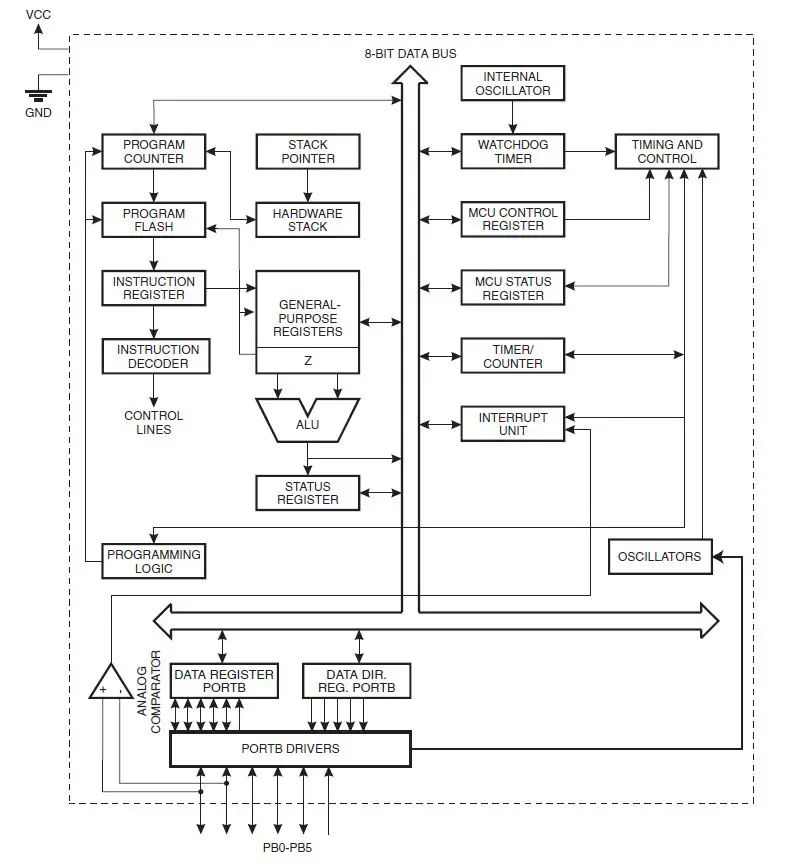
ATtiny12 Block Diagram
Figure 2 on page 4. The ATtiny12 provides the following features: 1K bytes of Flash, 64 bytes EEPROM, up to six general-purpose I/O lines, 32 general-purpose working registers, an 8-bit timer/counter, internal and external interrupts, programmable Watchdog Timer with internal oscillator, and two software-selectable power-saving modes. The Idle Mode stops the CPU while allowing the timer/counters and interrupt system to continue functioning. The Power-down Mode saves the register contents but freezes the oscillator, disabling all other chip functions until the next interrupt or hardware reset. The wake-up or interrupt on pin change features enable the ATtiny12 to be highly responsive to external events, still featuring the lowest power consumption while in the power-down modes. The device is manufactured using Atmel’s high-density nonvolatile memory technology. By combining an RISC 8-bit CPU with Flash on a monolithic chip, the Atmel ATtiny12 is a powerful microcontroller that provides a highly-flexible and cost-effective solution to many embedded control applications.
Figure 2. The ATtiny12 Block Diagram
Pin Descriptions
- Supply voltage pin.
- Ground pin.
Port B is a 6-bit I/O port. PB4..0 are I/O pins that can provide internal pull-ups (selected for each bit). On ATtiny11, PB5 is input only. On ATtiny12, PB5 is input or open-drain output. The port pins are tri-stated when a reset condition becomes active, even if the clock is not running. The use of pins PB5..3 as input or I/O pins is limited, depending on reset and clock settings, as shown below.
Table 2. PB5..PB3 Functionality vs. Device Clocking Options
| Device Clocking Option | PB5 | PB4 | PB3 |
| External Reset Enabled | Used(1) | -(2) | – |
| External Reset Disabled | Input(3)/I/O(4) | – | – |
| External Crystal | – | Used | Used |
| External Low-frequency Crystal | – | Used | Used |
| External Ceramic Resonator | – | Used | Used |
| External RC Oscillator | – | I/O(5) | Used |
| External Clock | – | I/O | Used |
| Internal RC Oscillator | – | I/O | I/O |
Notes
- Used” means the pin is used for reset or clock purposes.
- means the pin function is unaffected by the option.
- Input means the pin is a port input pin.
- On ATtiny11, PB5 is input only. On ATtiny12, PB5 is input or open-drain output.
- I/O means the pin is a port input/output pin.
XTAL1 Input to the inverting oscillator amplifier and input to the internal clock operating circuit.
XTAL2 Output from the inverting oscillator amplifier.
RESET Reset input. An external reset is generated by a low level on the RESET pin. Reset pulses longer than 50 ns will generate a reset, even if the clock is not running. Shorter pulses are not guaranteed to generate a reset.
Register Summary ATtiny11
| Address | Name | Bit 7 | Bit 6 | Bit 5 | Bit 4 | Bit 3 | Bit 2 | Bit 1 | Bit 0 | Page |
| $3F | SREG | I | T | H | S | V | N | Z | C | page 9 |
| $3E | Reserved | |||||||||
| $3D | Reserved | |||||||||
| $3C | Reserved | |||||||||
| $3B | GIMSK | – | INT0 | PCIE | – | – | – | – | – | page 33 |
| $3A | GIFR | – | INTF0 | PCIF | – | – | – | – | – | page 34 |
| $39 | TIMSK | – | – | – | – | – | – | TOIE0 | – | page 34 |
| $38 | TIFR | – | – | – | – | – | – | TOV0 | – | page 35 |
| $37 | Reserved | |||||||||
| $36 | Reserved | |||||||||
| $35 | MCUCR | – | – | SE | SM | – | – | ISC01 | ISC00 | page 32 |
| $34 | MCUSR | – | – | – | – | – | – | EXTRF | PORF | page 28 |
| $33 | TCCR0 | – | – | – | – | – | CS02 | CS01 | CS00 | page 41 |
| $32 | TCNT0 | Timer/Counter0 (8 Bit) | page 41 | |||||||
| $31 | Reserved | |||||||||
| $30 | Reserved | |||||||||
| … | Reserved | |||||||||
| $22 | Reserved | |||||||||
| $21 | WDTCR | – | – | – | WDTOE | WDE | WDP2 | WDP1 | WDP0 | page 43 |
| $20 | Reserved | |||||||||
| $1F | Reserved | |||||||||
| $1E | Reserved | |||||||||
| $1D | Reserved | |||||||||
| $1C | Reserved | |||||||||
| $1B | Reserved | |||||||||
| $1A | Reserved | |||||||||
| $19 | Reserved | |||||||||
| $18 | PORTB | – | – | – | PORTB4 | PORTB3 | PORTB2 | PORTB1 | PORTB0 | page 37 |
| $17 | DDRB | – | – | – | DDB4 | DDB3 | DDB2 | DDB1 | DDB0 | page 37 |
| $16 | PINB | – | – | PINB5 | PINB4 | PINB3 | PINB2 | PINB1 | PINB0 | page 37 |
| $15 | Reserved | |||||||||
| … | Reserved | |||||||||
| $0A | Reserved | |||||||||
| $09 | Reserved | |||||||||
| $08 | ACSR | ACD | – | ACO | ACI | ACIE | – | ACIS1 | ACIS0 | page 45 |
| … | Reserved | |||||||||
| $00 | Reserved | |||||||||
Notes
- For compatibility with future devices, reserved bits should be written to zero if accessed. Reserved I/O memory addresses should never be written.
- Some of the status flags are cleared by writing a logical one to them. Note that the CBI and SBI instructions will operate on all bits in the I/O register, writing a one back into any flag read as set, thus clearing the flag. The CBI and SBI instructions work with registers $00 to $1F only.
Register Summary ATtiny12
| Address | Name | Bit 7 | Bit 6 | Bit 5 | Bit 4 | Bit 3 | Bit 2 | Bit 1 | Bit 0 | Page |
| $3F | SREG | I | T | H | S | V | N | Z | C | page 9 |
| $3E | Reserved | |||||||||
| $3D | Reserved | |||||||||
| $3C | Reserved | |||||||||
| $3B | GIMSK | – | INT0 | PCIE | – | – | – | – | – | page 33 |
| $3A | GIFR | – | INTF0 | PCIF | – | – | – | – | – | page 34 |
| $39 | TIMSK | – | – | – | – | – | – | TOIE0 | – | page 34 |
| $38 | TIFR | – | – | – | – | – | – | TOV0 | – | page 35 |
| $37 | Reserved | |||||||||
| $36 | Reserved | |||||||||
| $35 | MCUCR | – | PUD | SE | SM | – | – | ISC01 | ISC00 | page 32 |
| $34 | MCUSR | – | – | – | – | WDRF | BORF | EXTRF | PORF | page 29 |
| $33 | TCCR0 | – | – | – | – | – | CS02 | CS01 | CS00 | page 41 |
| $32 | TCNT0 | Timer/Counter0 (8 Bit) | page 41 | |||||||
| $31 | OSCCAL | Oscillator Calibration Register | page 12 | |||||||
| $30 | Reserved | |||||||||
| … | Reserved | |||||||||
| $22 | Reserved | |||||||||
| $21 | WDTCR | – | – | – | WDTOE | WDE | WDP2 | WDP1 | WDP0 | page 43 |
| $20 | Reserved | |||||||||
| $1F | Reserved | |||||||||
| $1E | EEAR | – | – | EEPROM Address Register | page 18 | |||||
| $1D | EEDR | EEPROM Data Register | page 18 | |||||||
| $1C | EECR | – | – | – | – | EERIE | EEMWE | EEWE | EERE | page 18 |
| $1B | Reserved | |||||||||
| $1A | Reserved | |||||||||
| $19 | Reserved | |||||||||
| $18 | PORTB | – | – | – | PORTB4 | PORTB3 | PORTB2 | PORTB1 | PORTB0 | page 37 |
| $17 | DDRB | – | – | DDB5 | DDB4 | DDB3 | DDB2 | DDB1 | DDB0 | page 37 |
| $16 | PINB | – | – | PINB5 | PINB4 | PINB3 | PINB2 | PINB1 | PINB0 | page 37 |
| $15 | Reserved | |||||||||
| … | Reserved | |||||||||
| $0A | Reserved | |||||||||
| $09 | Reserved | |||||||||
| $08 | ACSR | ACD | AINBG | ACO | ACI | ACIE | – | ACIS1 | ACIS0 | page 45 |
| … | Reserved | |||||||||
| $00 | Reserved | |||||||||
Note
- For compatibility with future devices, reserved bits should be written to zero if accessed. Reserved I/O memory addresses should never be written.
- Some of the status flags are cleared by writing a logical one to them. Note that the CBI and SBI instructions will operate on all bits in the I/O register, writing a one back into any flag read as set, thus clearing the flag. The CBI and SBI instructions work with registers $00 to $1F only.
Instruction Set Summary
| Mnemonics | Operands | Description | Operation | Flags | #Clocks |
| ARITHMETIC AND LOGIC INSTRUCTIONS | |||||
| ADD | Rd, Rr | Add two Registers | Rd ¬ Rd + Rr | Z,C,N,V,H | 1 |
| ADC | Rd, Rr | Add with Carry two Registers | Rd ¬ Rd + Rr + C | Z,C,N,V,H | 1 |
| SUB | Rd, Rr | Subtract two Registers | Rd ¬ Rd – Rr | Z,C,N,V,H | 1 |
| SUBI | Rd, K | Subtract Constant from Register | Rd ¬ Rd – K | Z,C,N,V,H | 1 |
| SBC | Rd, Rr | Subtract with Carry two Registers | Rd ¬ Rd – Rr – C | Z,C,N,V,H | 1 |
| SBCI | Rd, K | Subtract with Carry Constant from Reg. | Rd ¬ Rd – K – C | Z,C,N,V,H | 1 |
| AND | Rd, Rr | Logical AND Registers | Rd ¬ Rd · Rr | Z,N,V | 1 |
| ANDI | Rd, K | Logical AND Register and Constant | Rd ¬ Rd · K | Z,N,V | 1 |
| OR | Rd, Rr | Logical OR Registers | Rd ¬ Rd v Rr | Z,N,V | 1 |
| ORI | Rd, K | Logical OR Register and Constant | Rd ¬ Rd v K | Z,N,V | 1 |
| EOR | Rd, Rr | Exclusive OR Registers | Rd ¬ RdÅRr | Z,N,V | 1 |
| COM | Rd | One’s Complement | Rd ¬ $FF – Rd | Z,C,N,V | 1 |
| NEG | Rd | Two’s Complement | Rd ¬ $00 – Rd | Z,C,N,V,H | 1 |
| SBR | Rd,K | Set Bit(s) in Register | Rd ¬ Rd v K | Z,N,V | 1 |
| CBR | Rd,K | Clear Bit(s) in Register | Rd ¬ Rd · (FFh – K) | Z,N,V | 1 |
| INC | Rd | Increment | Rd ¬ Rd + 1 | Z,N,V | 1 |
| DEC | Rd | Decrement | Rd ¬ Rd – 1 | Z,N,V | 1 |
| TST | Rd | Test for Zero or Minus | Rd ¬ Rd · Rd | Z,N,V | 1 |
| CLR | Rd | Clear Register | Rd ¬ RdÅRd | Z,N,V | 1 |
| SER | Rd | Set Register | Rd ¬ $FF | None | 1 |
| BRANCH INSTRUCTIONS | |||||
| RJMP | k | Relative Jump | PC ¬ PC + k + 1 | None | 2 |
| RCALL | k | Relative Subroutine Call | PC ¬ PC + k + 1 | None | 3 |
| RET | Subroutine Return | PC ¬ STACK | None | 4 | |
| RETI | Interrupt Return | PC ¬ STACK | I | 4 | |
| CPSE | Rd,Rr | Compare, Skip if Equal | if (Rd = Rr) PC ¬ PC + 2 or 3 | None | 1/2 |
| CP | Rd,Rr | Compare | Rd – Rr | Z, N,V,C,H | 1 |
| CPC | Rd,Rr | Compare with Carry | Rd – Rr – C | Z, N,V,C,H | 1 |
| CPI | Rd,K | Compare Register with Immediate | Rd – K | Z, N,V,C,H | 1 |
| SBRC | Rr, b | Skip if Bit in Register Cleared | if (Rr(b)=0) PC ¬ PC + 2 or 3 | None | 1/2 |
| SBRS | Rr, b | Skip if Bit in Register is Set | if (Rr(b)=1) PC ¬ PC + 2 or 3 | None | 1/2 |
| SBIC | P, b | Skip if Bit in I/O Register Cleared | if (P(b)=0) PC ¬ PC + 2 or 3 | None | 1/2 |
| SBIS | P, b | Skip if Bit in I/O Register is Set | if (P(b)=1) PC ¬ PC + 2 or 3 | None | 1/2 |
| BRBS | s, k | Branch if Status Flag Set | if (SREG(s) = 1) then PC¬PC + k + 1 | None | 1/2 |
| BRBC | s, k | Branch if Status Flag Cleared | if (SREG(s) = 0) then PC¬PC + k + 1 | None | 1/2 |
| BREQ | k | Branch if Equal | if (Z = 1) then PC ¬ PC + k + 1 | None | 1/2 |
| BRNE | k | Branch if Not Equal | if (Z = 0) then PC ¬ PC + k + 1 | None | 1/2 |
| BRCS | k | Branch if Carry Set | if (C = 1) then PC ¬ PC + k + 1 | None | 1/2 |
| BRCC | k | Branch if Carry Cleared | if (C = 0) then PC ¬ PC + k + 1 | None | 1/2 |
| BRSH | k | Branch if Same or Higher | if (C = 0) then PC ¬ PC + k + 1 | None | 1/2 |
| BRLO | k | Branch if Lower | if (C = 1) then PC ¬ PC + k + 1 | None | 1/2 |
| BRMI | k | Branch if Minus | if (N = 1) then PC ¬ PC + k + 1 | None | 1/2 |
| BRPL | k | Branch if Plus | if (N = 0) then PC ¬ PC + k + 1 | None | 1/2 |
| BRGE | k | Branch if Greater or Equal, Signed | if (N Å V= 0) then PC ¬ PC + k + 1 | None | 1/2 |
| BRLT | k | Branch if Less Than Zero, Signed | if (N Å V= 1) then PC ¬ PC + k + 1 | None | 1/2 |
| BRHS | k | Branch if Half Carry Flag Set | if (H = 1) then PC ¬ PC + k + 1 | None | 1/2 |
| BRHC | k | Branch if Half Carry Flag Cleared | if (H = 0) then PC ¬ PC + k + 1 | None | 1/2 |
| BRTS | k | Branch if T Flag Set | if (T = 1) then PC ¬ PC + k + 1 | None | 1/2 |
| BRTC | k | Branch if T Flag Cleared | if (T = 0) then PC ¬ PC + k + 1 | None | 1/2 |
| BRVS | k | Branch if Overflow Flag is Set | if (V = 1) then PC ¬ PC + k + 1 | None | 1/2 |
| BRVC | k | Branch if Overflow Flag is Cleared | if (V = 0) then PC ¬ PC + k + 1 | None | 1/2 |
| BRIE | k | Branch if Interrupt Enabled | if ( I = 1) then PC ¬ PC + k + 1 | None | 1/2 |
| BRID | k | Branch if Interrupt Disabled | if ( I = 0) then PC ¬ PC + k + 1 | None | 1/2 |
| Mnemonics | Operands | Description | Operation | Flags | #Clocks |
| DATA TRANSFER INSTRUCTIONS | |||||
| LD | Rd,Z | Load Register Indirect | Rd ¬ (Z) | None | 2 |
| ST | Z,Rr | Store Register Indirect | (Z) ¬ Rr | None | 2 |
| MOV | Rd, Rr | Move Between Registers | Rd ¬ Rr | None | 1 |
| LDI | Rd, K | Load Immediate | Rd ¬ K | None | 1 |
| IN | Rd, P | In Port | Rd ¬ P | None | 1 |
| OUT | P, Rr | Out Port | P ¬ Rr | None | 1 |
| LPM | Load Program Memory | R0 ¬ (Z) | None | 3 | |
| BIT AND BIT-TEST INSTRUCTIONS | |||||
| SBI | P,b | Set Bit in I/O Register | I/O(P,b) ¬ 1 | None | 2 |
| CBI | P,b | Clear Bit in I/O Register | I/O(P,b) ¬ 0 | None | 2 |
| LSL | Rd | Logical Shift Left | Rd(n+1) ¬ Rd(n), Rd(0) ¬ 0 | Z,C,N,V | 1 |
| LSR | Rd | Logical Shift Right | Rd(n) ¬ Rd(n+1), Rd(7) ¬ 0 | Z,C,N,V | 1 |
| ROL | Rd | Rotate Left Through Carry | Rd(0) ¬ C, Rd(n+1) ¬ Rd(n), C ¬ Rd(7) | Z,C,N,V | 1 |
| ROR | Rd | Rotate Right Through Carry | Rd(7) ¬ C, Rd(n) ¬ Rd(n+1), C ¬ Rd(0) | Z,C,N,V | 1 |
| ASR | Rd | Arithmetic Shift Right | Rd(n) ¬ Rd(n+1), n = 0..6 | Z,C,N,V | 1 |
| SWAP | Rd | Swap Nibbles | Rd(3..0) ¬ Rd(7..4), Rd(7..4) ¬ Rd(3..0) | None | 1 |
| BSET | s | Flag Set | SREG(s) ¬ 1 | SREG(s) | 1 |
| BCLR | s | Flag Clear | SREG(s) ¬ 0 | SREG(s) | 1 |
| BST | Rr, b | Bit Store from Register to T | T ¬ Rr(b) | T | 1 |
| BLD | Rd, b | Bit load from T to Register | Rd(b) ¬ T | None | 1 |
| SEC | Set Carry | C ¬ 1 | C | 1 | |
| CLC | Clear Carry | C ¬ 0 | C | 1 | |
| SEN | Set Negative Flag | N ¬ 1 | N | 1 | |
| CLN | Clear Negative Flag | N ¬ 0 | N | 1 | |
| SEZ | Set Zero Flag | Z ¬ 1 | Z | 1 | |
| CLZ | Clear Zero Flag | Z ¬ 0 | Z | 1 | |
| SEI | Global Interrupt Enable | I ¬ 1 | I | 1 | |
| CLI | Global Interrupt Disable | I ¬ 0 | I | 1 | |
| SES | Set Signed Test Flag | S ¬ 1 | S | 1 | |
| CLS | Clear Signed Test Flag | S ¬ 0 | S | 1 | |
| SEV | Set Twos Complement Overflow | V ¬ 1 | V | 1 | |
| CLV | Clear Twos Complement Overflow | V ¬ 0 | V | 1 | |
| SET | Set T in SREG | T ¬ 1 | T | 1 | |
| CLT | Clear T in SREG | T ¬ 0 | T | 1 | |
| SEH | Set Half Carry Flag in SREG | H ¬ 1 | H | 1 | |
| CLH | Clear Half Carry Flag in SREG | H ¬ 0 | H | 1 | |
| NOP | No Operation | None | 1 | ||
| SLEEP | Sleep | (see specific descr. for Sleep function) | None | 1 | |
| WDR | Watch Dog Reset | (see specific descr. for WDR/timer) | None | 1 | |
Ordering Information
ATtiny11
| Power Supply | Speed (MHz) | Ordering Code | Package | Operation Range |
|
2.7 – 5.5V |
2 | ATtiny11L-2PC ATtiny11L-2SC | 8P3 8S2 | Commercial (0°C to 70°C) |
| ATtiny11L-2PI ATtiny11L-2SI ATtiny11L-2SU(2) | 8P3 8S2 8S2 | Industrial (-40°C to 85°C) | ||
|
4.0 – 5.5V |
6 | ATtiny11-6PC ATtiny11-6SC | 8P3 8S2 | Commercial (0°C to 70°C) |
| ATtiny11-6PI ATtiny11-6PU(2) ATtiny11-6SI ATtiny11-6SU(2) | 8P3 8P3 8S2 8S2 | Industrial (-40°C to 85°C) |
Notes
- The speed grade refers to maximum clock rate when using an external crystal or external clock drive. The internal RC oscillator has the same nominal clock frequency for all speed grades.
- Pb-free packaging alternative, complies to the European Directive for Restriction of Hazardous Substances (RoHS directive). Also Halide free and fully Green.
| Package Type | |
| 8P3 | 8-lead, 0.300″ Wide, Plastic Dual Inline Package (PDIP) |
| 8S2 | 8-lead, 0.200″ Wide, Plastic Gull-Wing Small Outline (EIAJ SOIC) |
ATtiny12
| Power Supply | Speed (MHz) | Ordering Code | Package | Operation Range |
|
1.8 – 5.5V |
1.2 | ATtiny12V-1PC ATtiny12V-1SC | 8P3 8S2 | Commercial (0°C to 70°C) |
| ATtiny12V-1PI ATtiny12V-1PU(2) ATtiny12V-1SI ATtiny12V-1SU(2) | 8P3 8P3 8S2 8S2 | Industrial (-40°C to 85°C) | ||
|
2.7 – 5.5V |
4 | ATtiny12L-4PC ATtiny12L-4SC | 8P3 8S2 | Commercial (0°C to 70°C) |
| ATtiny12L-4PI ATtiny12L-4PU(2) ATtiny12L-4SI ATtiny12L-4SU(2) | 8P3 8P3 8S2 8S2 | Industrial (-40°C to 85°C) | ||
|
4.0 – 5.5V |
8 | ATtiny12-8PC ATtiny12-8SC | 8P3 8S2 | Commercial (0°C to 70°C) |
| ATtiny12-8PI ATtiny12-8PU(2) ATtiny12-8SI ATtiny12-8SU(2) | 8P3 8P3 8S2 8S2 | Industrial (-40°C to 85°C) |
Notes
- The speed grade refers to maximum clock rate when using an external crystal or external clock drive. The internal RC oscillator has the same nominal clock frequency for all speed grades.
- Pb-free packaging alternative, complies to the European Directive for Restriction of Hazardous Substances (RoHS directive). Also Halide free and fully Green.
| Package Type | |
| 8P3 | 8-lead, 0.300″ Wide, Plastic Dual Inline Package (PDIP) |
| 8S2 | 8-lead, 0.200″ Wide, Plastic Gull-Wing Small Outline (EIAJ SOIC) |
Packaging Information
8P3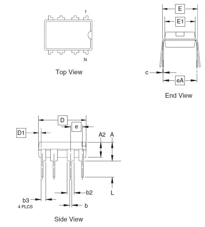
COMMON DIMENSIONS
(Unit of Measure = inches)
| SYMBOL | MIN | NOM | MAX | NOTE |
| A | 0.210 | 2 | ||
| A2 | 0.115 | 0.130 | 0.195 | |
| b | 0.014 | 0.018 | 0.022 | 5 |
| b2 | 0.045 | 0.060 | 0.070 | 6 |
| b3 | 0.030 | 0.039 | 0.045 | 6 |
| c | 0.008 | 0.010 | 0.014 | |
| D | 0.355 | 0.365 | 0.400 | 3 |
| D1 | 0.005 | 3 | ||
| E | 0.300 | 0.310 | 0.325 | 4 |
| E1 | 0.240 | 0.250 | 0.280 | 3 |
| e | 0.100 BSC | |||
| eA | 0.300 BSC | 4 | ||
| L | 0.115 | 0.130 | 0.150 | 2 |
Notes
- This drawing is for general information only; refer to JEDEC Drawing MS-001, Variation BA for additional information.
- Dimensions A and L are measured with the package seated in JEDEC seating plane Gauge GS-3.
- D, D1 and E1 dimensions do not include mold Flash or protrusions. Mold Flash or protrusions shall not exceed 0.010 inch.
- E and eA measured with the leads constrained to be perpendicular to datum.
- Pointed or rounded lead tips are preferred to ease insertion.
- b2 and b3 maximum dimensions do not include Dambar protrusions. Dambar protrusions shall not exceed 0.010 (0.25 mm).
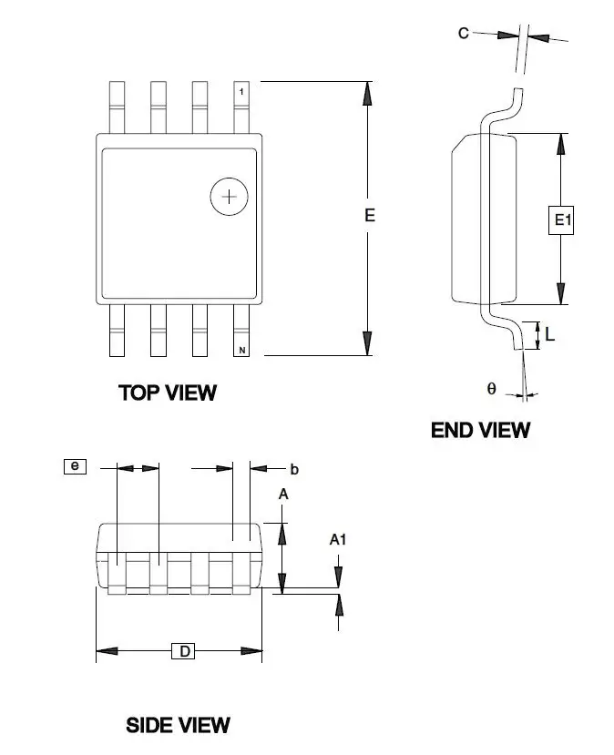
COMMON DIMENSIONS
(Unit of Measure = mm)
| SYMBOL | MIN | NOM | MAX | NOTE |
| A | 1.70 | 2.16 | ||
| A1 | 0.05 | 0.25 | ||
| b | 0.35 | 0.48 | 5 | |
| C | 0.15 | 0.35 | 5 | |
| D | 5.13 | 5.35 | ||
| E1 | 5.18 | 5.40 | 2, 3 | |
| E | 7.70 | 8.26 | ||
| L | 0.51 | 0.85 | ||
| q | 0° | 8° | ||
| e | 1.27 BSC | 4 | ||
Notes
- This drawing is for general information only; refer to EIAJ Drawing EDR-7320 for additional information.
- Mismatch of the upper and lower dies and resin burrs are not included.
- It is recommended that upper and lower cavities be equal. If they are different, the larger dimension shall be regarded.
- Determines the true geometric position.
- Values b,C apply to plated terminal. The standard thickness of the plating layer shall measure between 0.007 to .021 mm.
Datasheet Revision History
Please note that the page numbers listed in this section are refering to this document. The revision numbers are referring to the document revision.
Rev. 1006F-06/07
- Not recommended for new design”
Rev. 1006E-07/06
- Updated chapter layout.
- Updated Power-down in “Sleep Modes for the ATtiny11” on page 20.
- Updated Power-down in “Sleep Modes for the ATtiny12” on page 20.
- Updated Table 16 on page 36.
- Updated “Calibration Byte in ATtiny12” on page 49.
- Updated “Ordering Information” on page 10.
- Updated “Packaging Information” on page 12.
Rev. 1006D-07/03
- Updated VBOT values in Table 9 on page 24.
Rev. 1006C-09/01
- N/A
Headquarters International
- Atmel Corporation 2325 Orchard Parkway San Jose, CA 95131 USA Tel: 1(408) 441-0311 Fax: 1(408) 487-2600
- Atmel Asia Room 1219 Chinachem Golden Plaza 77 Mody Road Tsimshatsui East Kowloon Hong Kong Tel: (852) 2721-9778 Fax: (852) 2722-1369
- Atmel Europe Le Krebs 8, Rue Jean-Pierre Timbaud BP 309 78054 Saint-Quentin-en- Yvelines Cedex France Tel: (33) 1-30-60-70-00 Fax: (33) 1-30-60-71-11
- Atmel Japan 9F, Tonetsu Shinkawa Bldg. 1-24-8 Shinkawa Chuo-ku, Tokyo 104-0033 Japan Tel: (81) 3-3523-3551 Fax: (81) 3-3523-7581
Product Contact
Web Site www.atmel.com Technical Support [email protected] Sales Contact www.atmel.com/contacts Literature Requests www.atmel.com/literature
Disclaimer: The information in this document is provided in connection with Atmel products. No license, express or implied, by estoppel or otherwise, to any
intellectual property right is granted by this document or in connection with the sale of Atmel products. EXCEPT AS SET FORTH IN ATMEL’S TERMS AND CONDITIONS OF SALE LOCATED ON ATMEL’S WEB SITE, ATMEL ASSUMES NO LIABILITY WHATSOEVER AND DISCLAIMS ANY EXPRESS, IMPLIED OR STATUTORY
WARRANTY
RELATING TO ITS PRODUCTS INCLUDING, BUT NOT LIMITED TO, THE IMPLIED WARRANTY OF MERCHANTABILITY, FITNESS FOR A PARTICULAR
PURPOSE, OR NON-INFRINGEMENT. IN NO EVENT SHALL ATMEL BE LIABLE FOR ANY DIRECT, INDIRECT, CONSEQUENTIAL, PUNITIVE, SPECIAL OR INCIDENTAL DAMAGES (INCLUDING, WITHOUT LIMITATION, DAMAGES FOR LOSS OF PROFITS, BUSINESS INTERRUPTION, OR LOSS OF INFORMATION) ARISING OUT OF THE USE OR INABILITY TO USE THIS DOCUMENT, EVEN IF ATMEL HAS BEEN ADVISED OF THE POSSIBILITY OF SUCH DAMAGES. Atmel makes no representations or warranties with respect to the accuracy or completeness of the contents of this document and reserves the right to make changes to specifications and product descriptions at any time without notice. Atmel does not make any commitment to update the information contained herein. Unless specifically provided otherwise, Atmel products are not suitable for, and shall not be used in, automotive applications. Atmel’s products are not intended, authorized, or warranted for use as components in applications intended to support or sustain life.
© 2007 Atmel Corporation. All rights reserved. Atmel®, logo and combinations thereof, and others are registered trademarks or trademarks of Atmel Corporation or its subsidiaries. Other terms and product names may be trademarks of others.


