OMNIVISION WS4694C Image Sensor 
Descriptions
The WS4694C is a small, low RON, single channel load switch with controlled slew rate. The device operates over an input voltage range of 2.6 V to 5.5 V. The device supports current limit from 0.05 A to 2 A.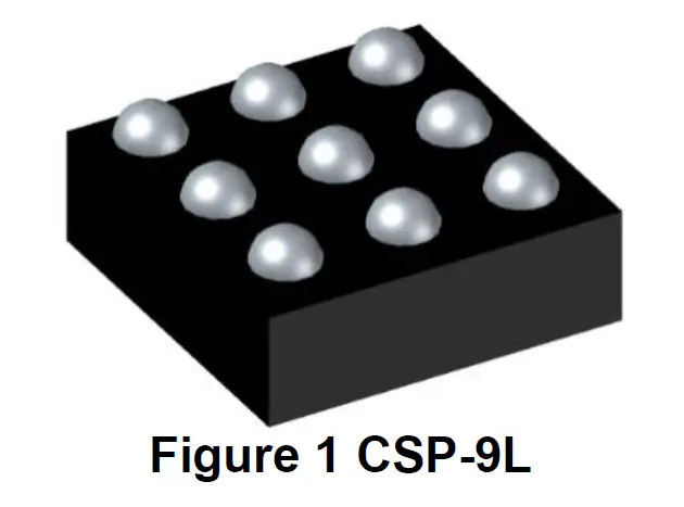
The controlled rising time of the device greatly reduces inrush current caused by large bulk load capacitance, thereby reducing or eliminating power supply drop. The WS4694C has a True Reverse-Current Blocking (TRCB) function that obstructs unwanted reverse current from VOUT to VIN during ON and OFF states. The small size and low RON device is designed for space constrained battery powered applications. The wide input voltage range of the switch makes it a versatile solution for many different voltage rails.
The WS4694C are available in a CSP-9L package. Standard products are Pb-free and Halogen-free.
Features
- Input Voltage Range: 2.6 V ~ 5.5 V
- Absolute Rating at VOUT: 28 V
- Maximum Output current: 2.0 A
- Adjustable Current Limit: 0.05 A ~ 2.0 A
1 A ~2.0 A with 15% Accuracy - True Reverse-Current Blocking (TRCB)
- Under-Voltage Lockout and Thermal Shutdown
- CSP-9L
Order Information
Table 1
| Device | Package | Shipping |
| WS4694C-9/TR | CSP-9L | 3000/Reel&Tape |
Applications
- Smart Phones, Tablet PCs
- Storage, DSLRs, and other portable devices
Pin Information 
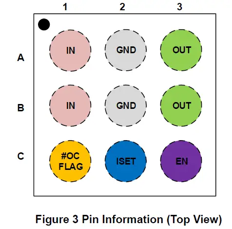
Table 2
| Pin | Symbol | Description |
| A3, B3 | OUT | Output pin |
| A1, B1 | IN | Input pin |
| A2, B2 | GND | Ground |
| C3 | EN | ON/OFF Control Input: Active HIGH |
| C2 | ISET | Current Limit Set Input: A resistor from ISET to ground sets the current limit for the switch. |
| C1 | #OCFLAG | Fault Output: Active LOW, open-drain output that indicates an input over current. An external pull-up resistor to VDD is required. |
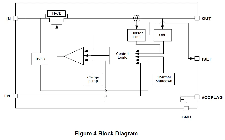
Block Diagram 
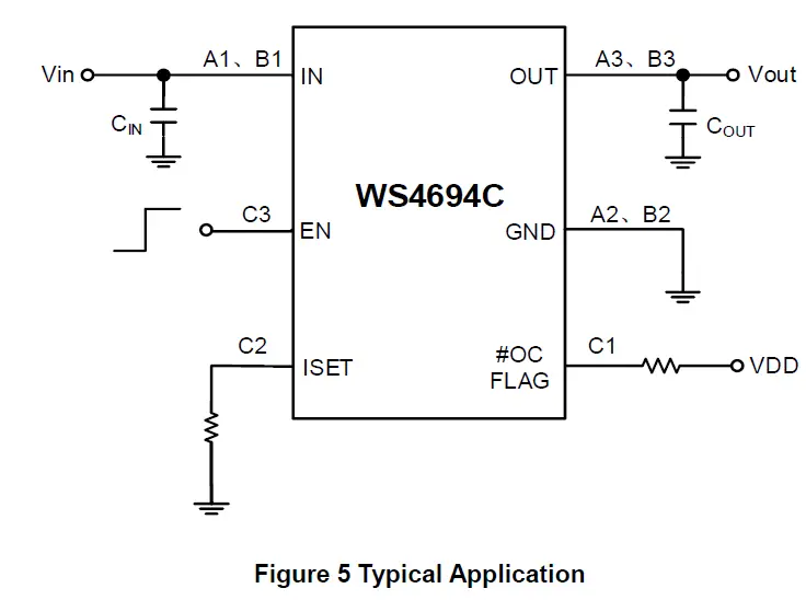
Typical Application 
Absolute Maximum Ratings
These are stress ratings only. Stresses exceeding the range specified in Table 3 might cause substantial damage to the device. Functional operation of the device at other conditions beyond those listed in the specification is not implied. Prolonged exposure to extreme conditions might affect device reliability.
Table 3
| Parameter | Symbol | Min. | Max. | Unit |
| VOUT to GND, VOUT to VIN | OUT | -0.3 | 28 | V |
| Other Pins to GND | IN, EN, ISET, #OCFLAG | -0.3 | 6 | V |
| Maximum Continuous Switch Current(1) | ISW | 2.3 | A | |
| Operating Junction Temperature | TJ | -40 | 150 | oC |
| Storage Temperature Range | TSTG | -65 | 150 | oC |
| Lead Temperature | TL | 260 | oC | |
|
ESD Ratings | HBM | 5 | kV | |
| CDM | 2 | kV | ||
| Air Discharge (VIN, VOUT to GND) | 15 | kV | ||
| Contact Discharge (VIN, VOUT to GND) | 8 | kV | ||
Maximum Junction Temperature = 85°C
Recommend Operation Ratings
The following table defines the conditions for actual device operation. Recommended operating conditions are specified to ensure optimal performance to the datasheet specifications.
Table 4
| Parameter | Symbol | Min. | Max. | Unit |
| Supply Voltage | VIN | 2.6 | 5.5 | V |
| Other Pins | EN, ISET, #OCFLAG | 2.5 | 5.5 | V |
| Operating Ambient Temperature | TA | -40 | 85 | oC |
| Thermal Resistance, RθJA (CSP-9L)(2) | RθJA | 110 | oC/W | |
Surface mounted on FR-4 Board using 2 oz, 1 square inch Cu area, PCB board size 1.5*1.5 square inches.
Electrical Characteristics
TA = -40 to +85°C, VIN = 2.6 to 5.5 V, Typical values are at VIN = 5 V and TA = 25oC, unless otherwise noted.
Table 5
| Parameter | Symbol | Condition | Min. | Typ. | Max. | Unit |
| Basic Operation | ||||||
| Input Voltage | VIN | 2.6 | 5.5 | V | ||
| Quiescent Current | IQ | VIN= VEN, VOUT=Open, TA=25oC | 80 | 150 | µA | |
| Shutdown Current | ISD | VIN=5.5 V, VOUT=0 V, VEN=GND | 0.1 | µA | ||
| Off Supply Current | IQ(OFF) | VEN=GND, VOUT=Open | 1 | µA | ||
|
On Resistance |
RON | VIN=VEN=5 V, IOUT=1 A, TA=25oC | 75 | 100 |
mΩ | |
| VIN=VEN=3.7 V, IOUT=1 A, TA=25oC | 85 | 105 | ||||
| EN Logic High Voltage | VIH | VIN=5 V, IOUT=0.1 A | 1.1 | V | ||
| EN Logic Low Voltage | VIL | VIN=5 V, IOUT=0.1 A | 0.4 | V | ||
| #OCFLAG Output Logic Low Voltage | VIL_FLAG | VIN=5 V, ISINK=10 mA | 0.1 | 0.2 | V | |
| VIN=2.6 V, ISINK=10 mA | 0.15 | 0.3 | V | |||
| #OCFLAG Output Logic High Leakage Current | IFLAG_LK | VIN=5 V, Switch on | 0.1 | 1 | µA | |
| EN Input Leakage | ION | VEN=0 V to VIN | 1 | µA | ||
| Pull-Down Resistance at EN Pin | REN_PD | VIN=2.6~5.5 V, VEN=High TA= –40 to 85oC | 14 | MΩ | ||
| Over-Voltage Protection | ||||||
| Output OVP Lockout | VOV_TRIP | VOUT Rising Threshold | 5.5 | 5.8 | 6 | V |
| VOUT Falling Threshold | 5.5 | |||||
| Output OVP Hysteresis | OUTHYS | 0.3 | V | |||
| OVP Response Time(3) | tOVP | IOUT=0.5 A, CL=1 µF, TA=25oC, VOUT from 5.5 V to 6.0 V | 1 | 4 | µs | |
| Over-Current Protection | ||||||
| Current Limit | ILIM | VIN=VEN=5 V, RSET=1000 Ω | 850 | 1000 | 1150 | mA |
| VIN=VEN=5 V, RSET=500 Ω | 1700 | 2000 | 2300 | |||
| Under-Voltage Lockout | VUVLO | VIN Increasing | 2.4 | V | ||
| VIN Decreasing | 2.2 | |||||
| UVLO Hysteresis | VUVLO_HYS | 200 | mV | |||
| RCB Protection Trip Point | VT_RCB | VOUT – VIN | 50 | mV | ||
| Parameter | Symbol | Condition | Min. | Typ. | Max. | Unit |
| RCB Protection Release Trip Point | VR_RCB | VIN – VOUT | 50 | mV | ||
| RCB Hysteresis | VRCB_HYS | 100 | mV | |||
| Default RCB Response Time(3) | tRCB | VIN=5 V, VEN=High/Low | 2 | µs | ||
| RCB Current | IRCB | VEN=0 V, VOUT=5.5 V | 7 | µA | ||
| Hard Over-Current Response Time(3) | tHOCP | Moderate Over-Current Condition, IOUT ≥ ILIM, VOUT=0 V | 2 | µs | ||
| Over-Current Response Time(3) | tOCP | Moderate Over-Current Condition, IOUT ≥ ILIM, VOUT ≤ VIN | 25 | µs | ||
| Over-Current Flag Response Time | tOC_FLAG | When Over-Current Occurs to Flag Pulling LOW | 8 | ms | ||
| Thermal Shutdown | TSD | Shutdown Threshold | 150 | oC | ||
| Return from Shutdown | 130 | |||||
| Hysteresis | 20 | |||||
| Turn-On Delay | TDON |
VIN=5 V, RL=100 Ω, CL=1 uF RSET=2000 Ω, TA=25oC | 0.8 | ms | ||
| VOUT Rise Time | TR | 0.3 | ||||
| Turn-On Time | TON | 1.1 | ||||
| Turn-Off Delay | TDOFF | 10 | µs | |||
| VOUT Fall Time | TF | 270 | ||||
| Turn-Off Time | TOFF | 280 | ||||
| Turn-On Delay | TDON |
VIN=5 V, RL=3.8 Ω, CL=10 uF RSET=600 Ω, TA=-40 to 85oC | 0.8 | ms | ||
| VOUT Rise Time | TR | 0.5 | ||||
| Turn-On Time | TON | 1.3 | ||||
| Turn-Off Delay | TDOFF | 10 | µs | |||
| VOUT Fall Time | TF | 230 | ||||
| Turn-Off Time | TOFF | 240 |
This parameter is guaranteed by design.
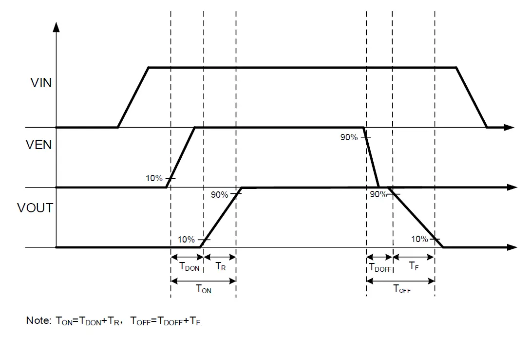
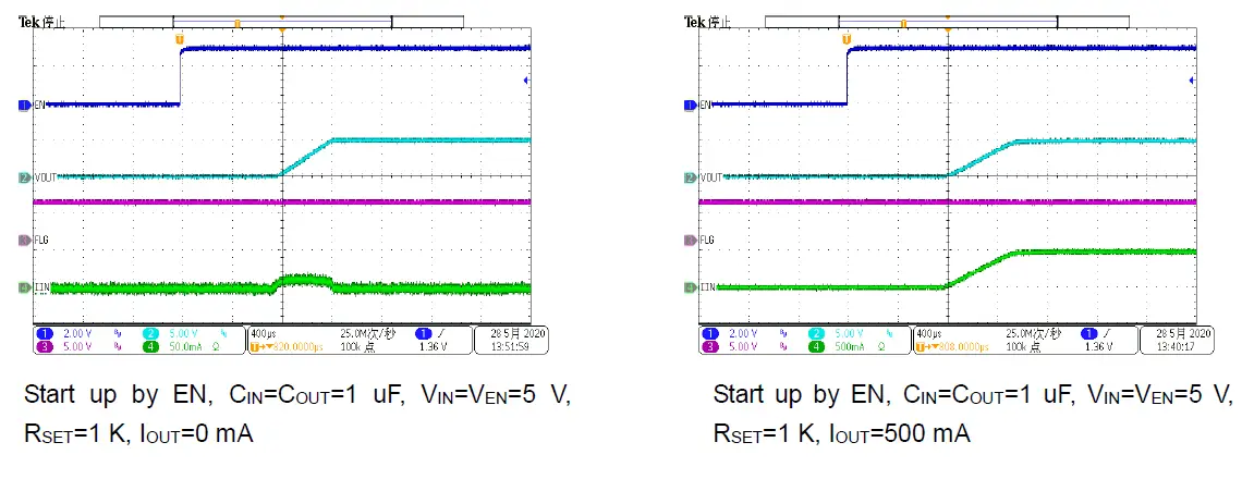
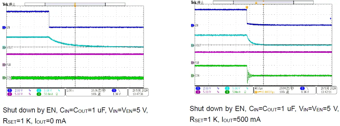
Timing Diagram 
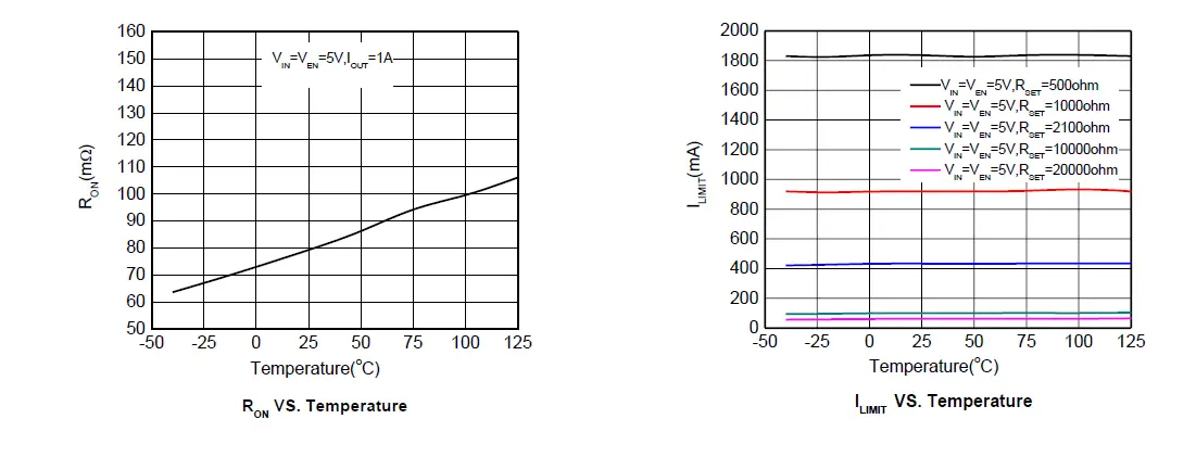
Typical characteristics
TA = 25oC, VIN = VEN = 5 V, CIN = 1 μF, COUT = 1 μF, unless otherwise noted. 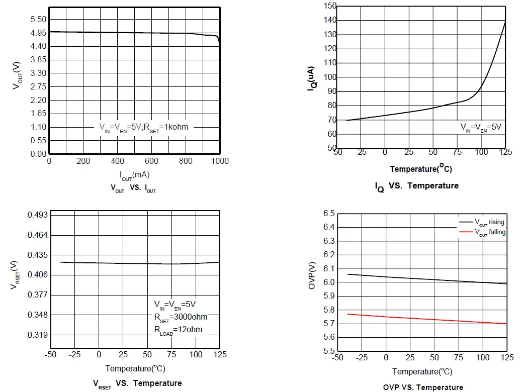

Application Information
Input Capacitor
To limit the voltage drop on the input supply caused by transient in-rush currents when the switch turns on, a capacitor needs to be placed between the VIN and the GND. Higher values of CIN can be used to further reduce the voltage drop in high-current applications.
Output capacitor
An output capacitor needs to be placed between the VOUT and the GND pin. The capacitor prevents parasitic board inductance from forcing VOUT below GND when the switch is on. The capacitor also prevents reverse inrush current from a voltage spike that could damage the device in the case of a VOUT short.
Fault Reporting
Upon the detection of an over-current, #OC_FLAG signals the fault by activating LOW.
Current Limiting
The current limit ensures that the current through the switch does not exceed the maximum set value, while not limiting the minimum value. The current at which the part’s limit is adjustable through the selection of the external resistor connected to the ISET pin. Information for selecting the resistor is found in the section below. The device acts as a constant-current source when the load draws more than the maximum value set by the device until thermal shutdown occurs. The device recovers if the die temperature drops below the threshold.
Under-Voltage Lockout
The Under-Voltage Lockout (UVLO) turns off the switch if the input voltage drops below the lockout threshold. With the EN pin activated, the input voltage rising above the UVLO threshold releases the lockout and enables the switch.
True Reverse-Current Blocking
The true reverse-current blocking feature protects the input source against current flow from output to input regardless of whether the load switch is on or not.
Thermal Shutdown
The thermal shutdown protects the die from internally or externally generated excessive temperature. During an over-temperature condition, the switch is turned off. The switch automatically turns on again if the temperature of the die drops below the threshold temperature.
Setting Current Limit
The current limit is set with an external resistor connected between the ISET and GND pins.
The current limit is calculated as the following: 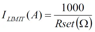
The resistor tolerance of 1% or less is recommended
Table 6 Current Limit Settings by RSET
| RSETΩ | Min. Current Limit (mA) | Typ. Current Limit (mA) | Max. Current Limit (mA) |
| 500 | 1700 | 2000 | 2300 |
| 571 | 1490 | 1750 | 2010 |
| 667 | 1275 | 1500 | 1725 |
| 800 | 1065 | 1250 | 1435 |
| 1000 | 850 | 1000 | 1150 |
| 1111 | 750 | 900 | 1050 |
| 1250 | 650 | 800 | 950 |
| 1429 | 550 | 700 | 850 |
| 1667 | 450 | 600 | 750 |
| 2000 | 350 | 500 | 650 |
Note: Table values are based on 1% tolerance resistors.
Layout Guide
For best performance, all traces need to be as short as possible. To be the most effective, the input and output capacitors need to be placed close to the device to minimize the effect that parasitic trace inductance might have on normal and short-circuit operation. Using wide traces for VIN, VOUT, GND helps minimize parasitic electrical effects along with the case-to-ambient thermal impedance.
Package Outline Dimensions 

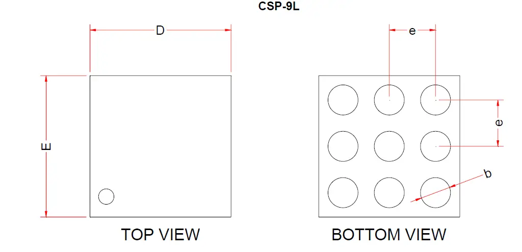
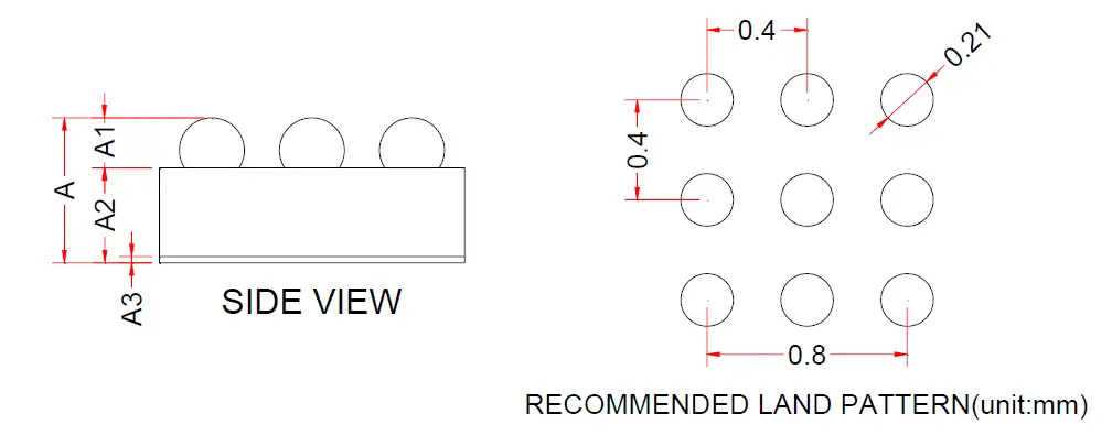
| Symbol | Dimensions in Millimeters | ||
| Min. | Typ. | Max. | |
| A | 0.54 | 0.58 | 0.63 |
| A1 | 0.18 | 0.20 | 0.22 |
| A2 | 0.36 | 0.38 | 0.41 |
| A3 | 0.025 Ref. | ||
| D | 1.19 | 1.22 | 1.25 |
| E | 1.19 | 1.22 | 1.25 |
| b | 0.24 | 0.26 | 0.28 |
| e | 0.40 BSC | ||
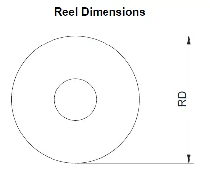
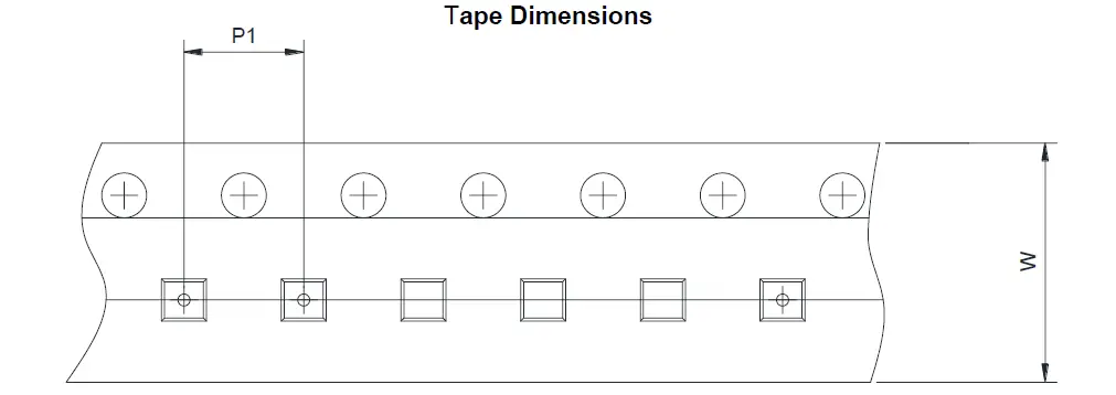
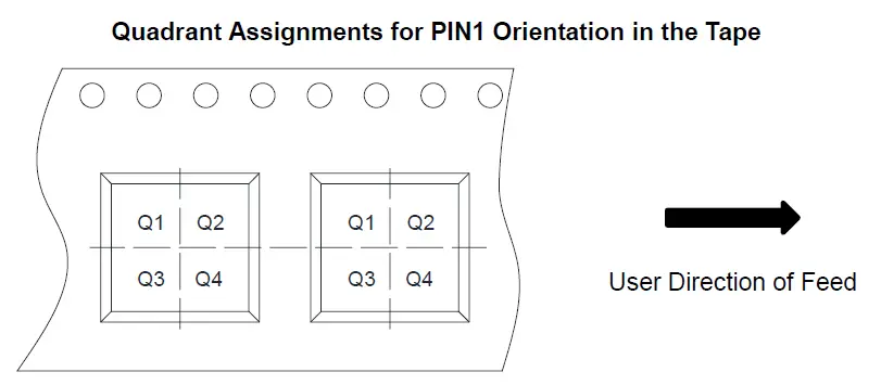
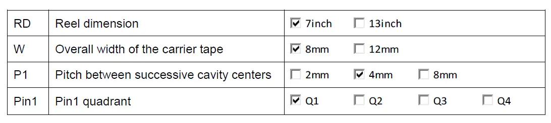
Tape And Reel Information 


4275 Burton Drive Santa Clara, CA 95054 USA
Tel: + 1 408 567 3000 Fax: + 1 408 567 3001 www.ovt.com
OMNIVISION reserves the right to make changes to their products or to discontinue any product or service without further notice. OMNIVISION and the OMNIVISION logo are trademarks or registered trademarks of OmniVision Technologies, Inc.
All other trademarks are the property of their respective owners.


