Fn-Link 3161A-SL Wi-Fi Single-band User Manual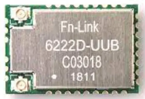
Overview
Introduction
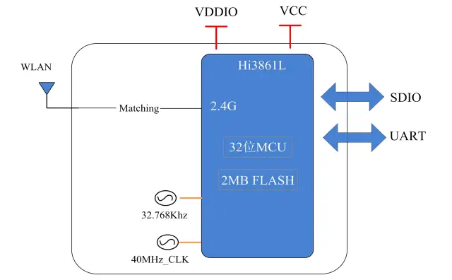
3161A-SL is a highly integrated 2.4 GHz Wi-Fi module that support the IEEE802.11b/g/nbaseband and RF circuit. It supports 20 MHz standard bandwidth and 5 MHz/10MHznarrow bandwidth, and provides a physical layer rate up to 72.2 Mbit/s. Wi-Fi baseband supports the orthogonal frequency division multiplexing (OFDM) technology and is backward compatible with the direct sequence spread spectrum(DSSS) and complementary code keying (CCK) technologies, offering various data rates defined in the IEEE 802.11 b/g/n protocol.
Module chipset integrates a high-performance 32-bit microprocessor, a hardware security engine, and various peripheral interfaces, including the SPI, UART, I2C, PWM,GPIO, and multi-channel ADC. In addition, it provides high-speed SDIO2.0slave interfaces, with clock frequency up to 50 MHz. Its built-in SRAM and flash can operate independently and even programming is allowed on the flash.
Block Diagram:
Features
- Operate at ISM frequency bands (2.4GHz)
- Maximum rate of 72.2 Mbit/s@HT20 MCS7
- SDIO interface for Wi-Fi
- Low power dissipation
- High transmitting power
- High receiving sensitivity
- PHY supporting IEEE 802.11b/g/n
- MAC supporting IEEE802.11 d/e/h/i/k/v/w
- Module integrated 32K clock
- WFA WPA, WFA WPA2 personal, and WPS2.0 for Wi-Fi
- Built-in 352 KB SRAM and 288 KB ROM
- Main chipset Built-in 32bit MCU and 2 MB flash memory
General Specification
| Model Name | 3161A-SL |
| Product Description | Support Wi-Fi functionality |
| Dimension | L x W x H: 12 x 12 x2.3 (typical) mm |
| Wi-Fi Interface | Support SDIO |
| Ambient temperature | -40°C to 85°C |
| Storage temperature | -40°C to 85°C |
| RoHS | All hardware components are fully compliant with EU RoHS directive |
Recommended Operating Rating
| Min. | Typ. | Max. | Unit | ||
| Ambient temperature | -40 | 25 | 85 | deg.C | |
| VCC | 2.3 | 3.3 | 3.6 | V | |
| VDDIO | – | 1.8V/3.3V | – | V | |
| Power Consumption | VCC = 3.3V(Unit:mA) | ||||
| Sleep Mode | 5uA | ||||
| TX Test mode (2.4G HT20@17dbm) | 288 | ||||
| RX Test mode (2.4G HT20) | 53 | ||||
Wi-Fi RF Specification
2.4GHz RF Specification
| Feature | Description | |||||
| WLAN Standard | IEEE 802.11 b/g/n Wi-Fi compliant | |||||
| Frequency Range | 2.400~2.4835GHz | |||||
| Number of Channels | Wi-Fi: US: channel 1~11; EU: channel 1~13; Japan: channel 1~14; | |||||
| Spectrum Mask | Min. b/g/n | Typ. b/g/n | Max. b/g/n | Unit b/g/n | ||
| 1st side lobes(to fc ± 11MHZ) | – | -43/-30/-40 | – | dBr | ||
| 2st side lobes(to fc ± 22MHZ) | – | -52/-33/-58 | – | dBr | ||
| Freq. Tolerance | -20/-20/-20 | – | 20/20/20 | ppm | ||
| Test Items | Typical Value | EVM | ||||
| Output Power | 802.11b /11Mbps : 16dBm ± 1.5 dB | EVM £ -10dB | ||||
| 802.11g /54Mbps : 16dBm ± 1.5 dB | EVM £ -25dB | |||||
| 802.11n /MCS7 | : 16dBm ± 1.5 dB | EVM £ -28dB | ||||
| Test Items | Test Value | Standard Value | ||||
| SISO Receive Sensitivity (11b,20MHz) @8% PER | – 1Mbps | PER @ -97 dBm | ≤-94 dBm | |||
| – 2Mbps | PER @ -95 dBm | ≤-92 dBm | ||||
| – 5.5Mbps | PER @ -92 dBm | ≤-89 dBm | ||||
| – 11Mbps | PER @ -90 dBm | ≤-87 dBm | ||||
|
SISO Receive Sensitivity (11g,20MHz) @10% PER | – 6Mbps | PER @ -94 dBm | ≤-89 dBm | |||
| – 9Mbps | PER @ -92 dBm | ≤-88 dBm | ||||
| – 12Mbps | PER @ -91 dBm | ≤-87 dBm | ||||
| – 18Mbps | PER @ -88 dBm | ≤-86 dBm | ||||
| – 24Mbps | PER @ -85 dBm | ≤-84 dBm | ||||
| – 36Mbps | PER @ -82 dBm | ≤-80 dBm | ||||
| – 48Mbps | PER @ -79 dBm | ≤-77 dBm | ||||
| – 54Mbps | PER @ -77 dBm | ≤-75 dBm | ||||
| SISO Receive Sensitivity (11n,20MHz) @10% PER | – MCS=0 | PER @ -93 dBm | ≤-89 dBm | |||
| – MCS=1 | PER @ -90 dBm | ≤-86 dBm | ||||
| – MCS=2 | PER @ -89 dBm | ≤-84 dBm | ||||
| – MCS=3 | PER @ -85 dBm | ≤-82 dBm | ||||
| – MCS=4 | PER @ -82 dBm | ≤-79 dBm | ||||
| – MCS=5 PER @ -78 dBm | ≤-76 dBm | |
| – MCS=6 PER @ -76 dBm | ≤-74 dBm | |
| – MCS=7 PER @ -73 dBm | ≤-72 dBm | |
| Maximum Input Level | 802.11b: -10 dBm | |
| 802.11g/n: -20 dBm | ||
| Antenna Reference | PCB antenna with 0~2 dBi peak gain | |
Pin Assignments
Pin Outline
TOP VIEW
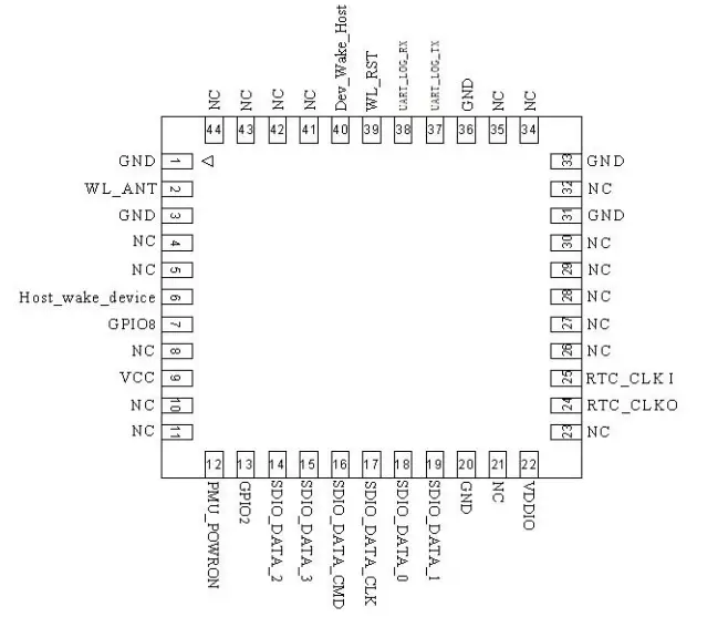
Pin Definition
| NO | Name | Type | Description | Voltage |
| 1 | GND | - | Ground connections | |
| 2 | WL_ANT | I/O | RF I/O port | |
| 3 | GND | - | Ground connections | |
| 4 | NC | - | Floating (Don’t connected to ground) | |
| 5 | NC | - | Floating (Don’t connected to ground) | |
| 6 | Host wake device | I | Host Wake up Wi-Fi,GPIO06 | VDDIO |
| 7 | GPIO8 | I/O | GPIO or configured as SDIO interrupt pin. (If not used keep Floating) | VDDIO |
| 8 | NC | - | Floating (Don’t connected to ground) | |
| 9 | VCC | P | Main power voltage source input 2.3V-3.6V | 3.3V |
| 10 | NC | - | Floating (Don’t connected to ground) | |
| 11 | NC | - | Floating (Don’t connected to ground) | |
| 12 | PMU_POWRON | I | Enable pin for WLAN device Defualt ON: pull high ; OFF: pull low | VDDIO |
| 13 | GPIO2 | I/O | SDIO data interrupt,or GPIO function. | VDDIO |
| 14 | SDIO_DATA_2 | I/O | SDIO data line 2, GPIO09 | VDDIO |
| 15 | SDIO_DATA_3 | I/O | SDIO data line 3, GPIO10 | VDDIO |
| 16 | SDIO_DATA_CMD | I/O | SDIO command line, GPIO11 | VDDIO |
| 17 | SDIO_DATA_CLK | I | SDIO clock line, GPIO12 | VDDIO |
| 18 | SDIO_DATA_0 | I/O | SDIO data line 0, GPIO13 | VDDIO |
| 19 | SDIO_DATA_1 | I/O | SDIO data line 1, GPIO14 | VDDIO |
| 20 | GND | - | Ground connections | |
| 21 | NC | - | Floating (Don’t connected to ground) | |
| 22 | VDDIO | P | I/O Voltage supply input 1.8V/3.3V | VDDIO |
| 23 | NC | - | Floating (Don’t connected to ground) | |
| 24 | RTC_CLK O | I/O | Floating(module have 32K clock), GPIO00 | VDDIO |
| 25 | RTC_CLK I | I | Floating(module have 32K clock), GPIO01 | VDDIO |
| 26 | NC | - | Floating (Don’t connected to ground) | |
| 27 | NC | - | Floating (Don’t connected to ground) | |
| 28 | NC | - | Floating (Don’t connected to ground) | |
| 29 | NC | - | Floating (Don’t connected to ground) | |
| 30 | NC | - | Floating (Don’t connected to ground) | |
| 31 | GND | - | Ground connections | |
| 32 | NC | - | Floating (Don’t connected to ground) |
| 33 | GND | - | Ground connections | |
| 34 | NC | – | Floating (Don’t connected to ground) | |
| 35 | NC | - | Floating (Don’t connected to ground) | |
| 36 | GND | - | Ground connections | |
| 37 | UART_LOG_TX | - | UART0_LOG_TX,GPIO03 For firmware download, can floating this pin | VDDIO |
| 38 | UART_LOG_RX | - | UART0_LOG_RX,GPIO04 For firmware download, can floating this pin | VDDIO |
| 39 | WL_RST | I | Wi-Fi reset pin. GPIO07 Low: reset enable, Defualt High: reset disable | VDDIO |
| 40 | Dev_Wake_Host | O | Wi-Fi wake up host. GPIO05 | VDDIO |
| 41 | NC | - | Floating (Don’t connected to ground) | |
| 42 | NC | - | Floating (Don’t connected to ground) | |
| 43 | NC | - | Floating (Don’t connected to ground) | |
| 44 | NC | - | Floating (Don’t connected to ground) |
Muti Pin definition
3861L all GPIO pin can configure as muti function,detail see below information.
| Pin | NAME | F.0 | F.1 | F.2 | F.3 | F.4 | F.5 | F.6 | F.7 | F.8 |
| 24 | GPIO00 | GPIO00 | UART1_TXD | SPI1_CLK | PWM3 | I2C1_SDA | RTC_OSC_32K | RTC32K_XOUT | / | / |
| 25 | GPIO01 | GPIO01 | UART1_RXD | SPI1_RXD | PWM4 | I2C1_SCL | / | RTC32K_XINT | / | / |
| 13 | GPIO02 | GPIO02 | UART1_RTS | SPI1_TXD | PWM2 | / | SSI_CLK | / | / | / |
| 37 | GPIO03 | UART0_LOG_TX | UART1_CTS | SPI1_CS1 | PWM5 | I2C1_SDA | SSI_DATA | GPIO03 | / | / |
| 38 | GPIO04 | UART0_LOG_RX | / | / | PWM1 | I2C1_SCL | / | GPIO04 | ADC1 | / |
| 40 | GPIO05 | UART1_RXD | GPIO05 | I2S0_MCK | PWM2 | / | BT_STATUS | SPI0_CS1 | ADC2 | / |
| 6 | GPIO06 | UART1_TXD | GPIO06 | I2S0_TX | PWM3 | / | COEX_SWITH | SPI0_CLK | / | / |
| 39 | GPIO07 | UART1_CTS | GPIO07 | I2S0_CLK | PWM0 | / | BT_ACTIVE | SPI0_RXD | ADC3 | / |
| 7 | GPIO08 | UART1_RTS | GPIO08 | I2S0_WS | PWM1 | / | WLAN_ACTIVE | SPI0_TXD | / | / |
| 14 | GPIO09 | GPIO09 | UART2_RTS | SPI0_TXD | PWM0 | I2C0_SCL | I2S0_MCK | SDIO_D2 | ADC4 | / |
| 15 | GPIO10 | GPIO10 | UART2_CTS | SPI0_CLK | PWM1 | I2C0_SDA | I2S0_TX | SDIO_D3 | / | / |
| 16 | GPIO11 | GPIO11 | UART2_TXD | SPI0_RXD | PWM2 | / | I2S0_RX | SDIO_CMD | ADC5 | / |
| 17 | GPIO12 | GPIO12 | UART2_RXD | SPI0_CS1 | PWM3 | / | I2S0_CLK | SDIO_CLK | ADC0 | / |
| 18 | GPIO13 | GPIO13 | UART2_RTS | UART0_LOG_TX | PWM4 | I2C0_SDA | I2S0_WS | SDIO_D0 | ADC6 | SSI_DATA |
| 19 | GPIO14 | GPIO14 | UART2_CTS | UART0_LOG_RX | PWM5 | I2C0_SCL | / | SDIO_D1 | / | SSI_CLK |
Notes:
- IO:Ispu/O.
- 1mA.
- 3/1.8V.
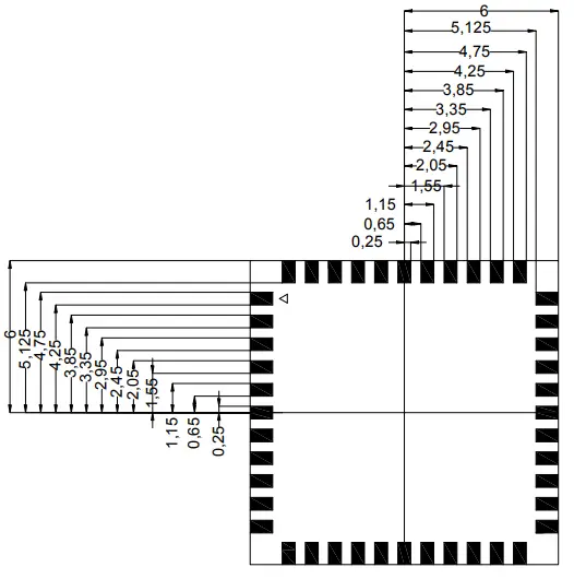
Dimensions
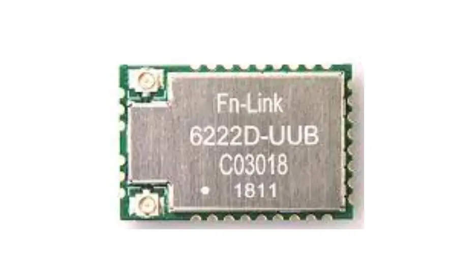
Module Picture
L x W : 12 x 12 (+0.3/-0.1) mm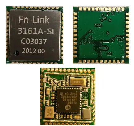
H: 2.3 (±0.2) mm
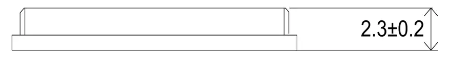
Weigh: 0.66g
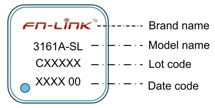
Marking Description
TOP VIEW
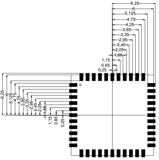
Module Physical Dimensions
Unit: mm
TOP VIEW
Layout Recommendation
(Unit: mm)
TOP VIEW
Host Interface Timing Diagram
SDIO Pin Description
The secure digital input/output (SDIO) interface supports three working modes:
Default speed mode (DS)
The maximum frequency of the interface clock is 25 MHz. The interface clock can work in 1-bit or 4-bit mode. High speed mode (HS)
The maximum frequency of the interface clock is 50 MHz. SDR25 mode
The maximum frequency of the interface clock is 50 MHz
SDIO Pin Description
SD 4-Bit Mode
DATA0 Data Line 0
DATA1 Data Line 1
DATA2 Data Line 2
DATA3 Data Line 3
CLK Clock
CMD Command Line
SDIO CLK Timing Diagram
DS Mode
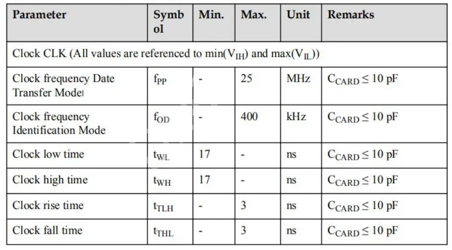
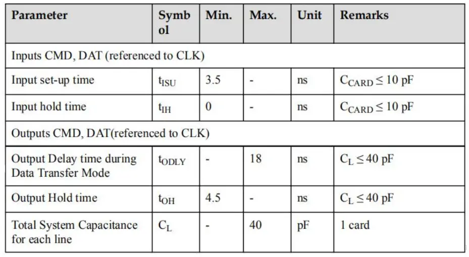
The DS mode is the default mode after the SDIO is powered on. To ensure compatibility with various host components, the DS mode requires a low working rate and supports only the 25MHz clock.
Clock parameters in DS mode (VDDIO=3.3 V)
Clock parameters in DS mode (VDDIO= 1.8 V)
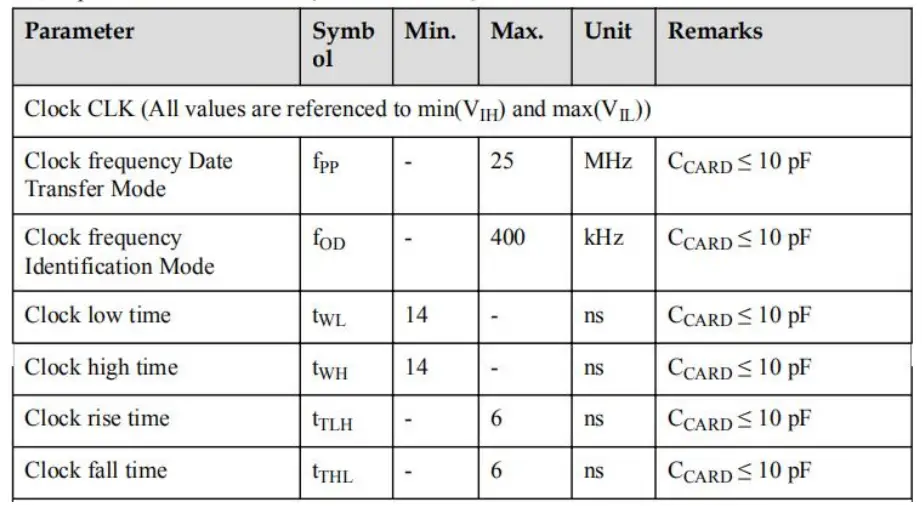
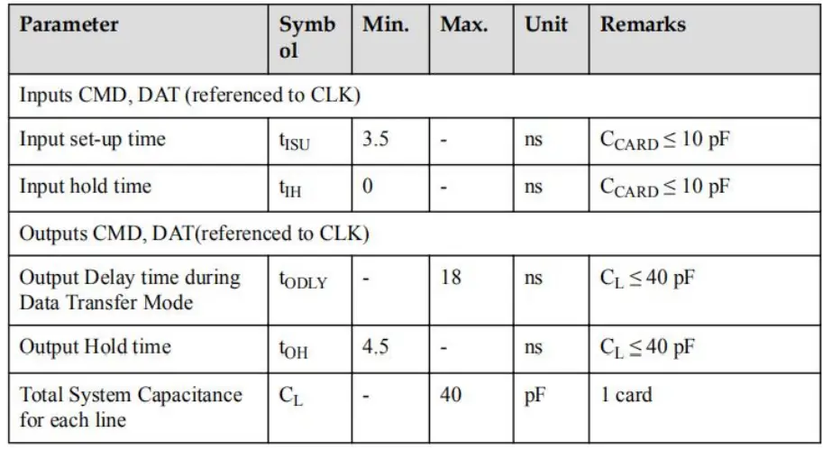
Figure 8-6 shows the output data timing in DS mode. tISU is the setup time, that is, the stability time required by the data of the SDIO interface before clock sampling in this mode. tIH is the hold time, that is, the time required by the data of the SDIO interface to retain the original level after clock sampling in this mode.
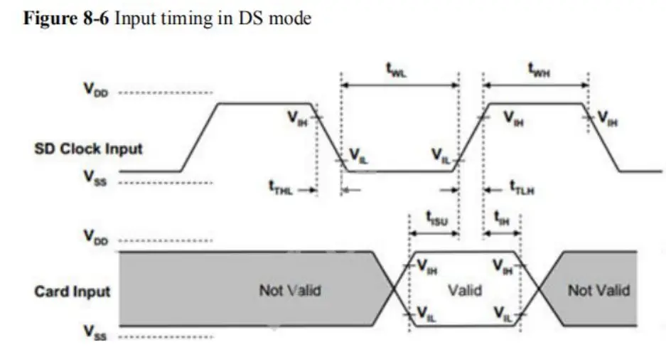
Figure 8-7 shows the input data timing in DS mode. Where, tODLY(max) is the maximum delay of the output data relative to the clock falling edge, and tODLY(min) is the minimum delay of the output data relative to the clock falling edge.
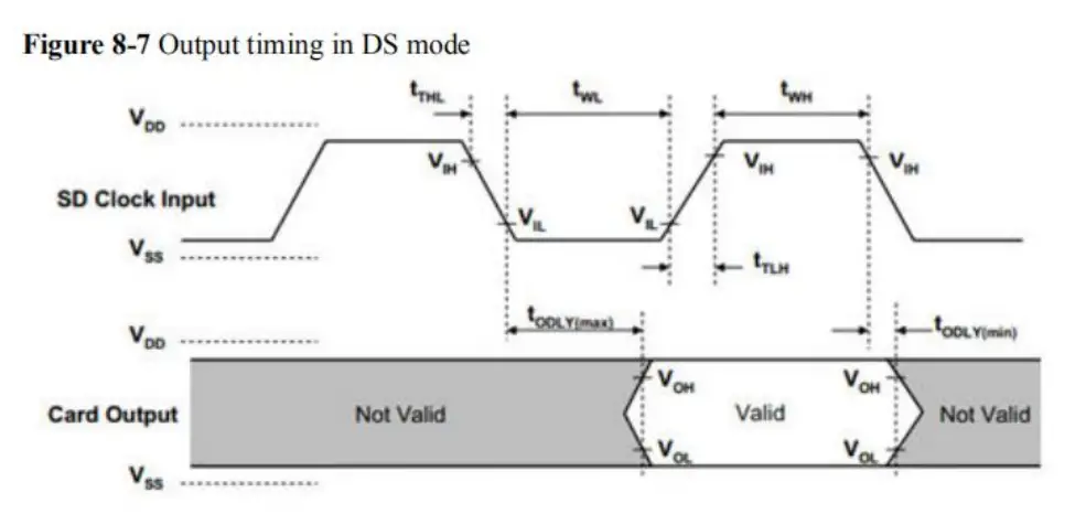
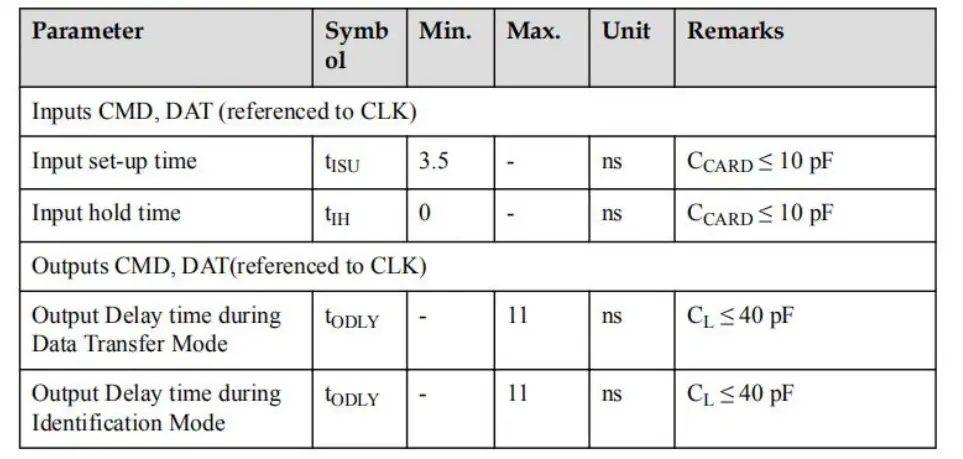
Table 8-12 describes the timing restrictions in DS mode.
Note: In DS mode, the output data is referenced to the clock falling edge, and the input data is referenced to the clock rising edge.
HS Mode
The HS mode is entered after the SDIO is powered on and initialized because a higher working rate than the DS mode is required. In HS mode, the clock supports 50 MHz. For details about the restrictions on the clock, see Table 8-13.
Table 8-13 Clock perimeters in HS ,ode (VDDIO = 3.3 V)
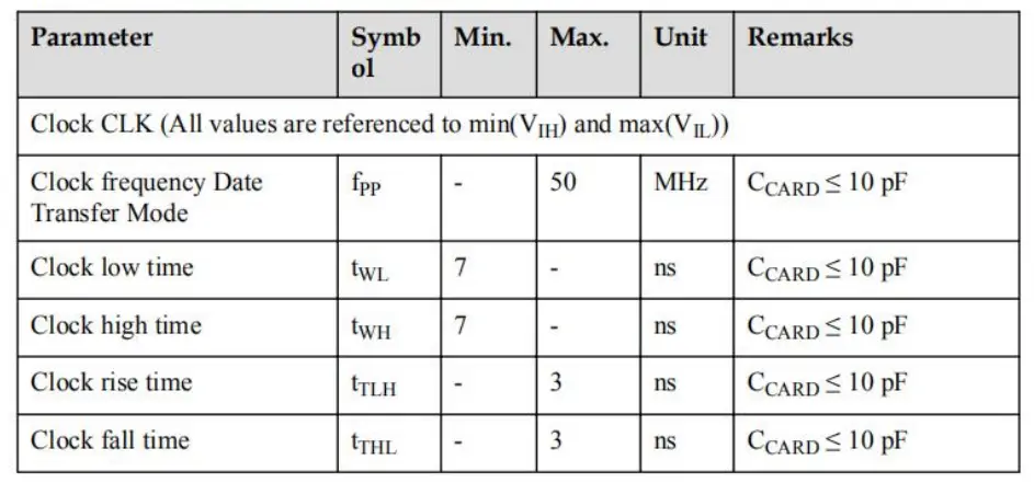
Table 8-14 Clock perimeters in HS mode (VDDIO = 1.8 V)
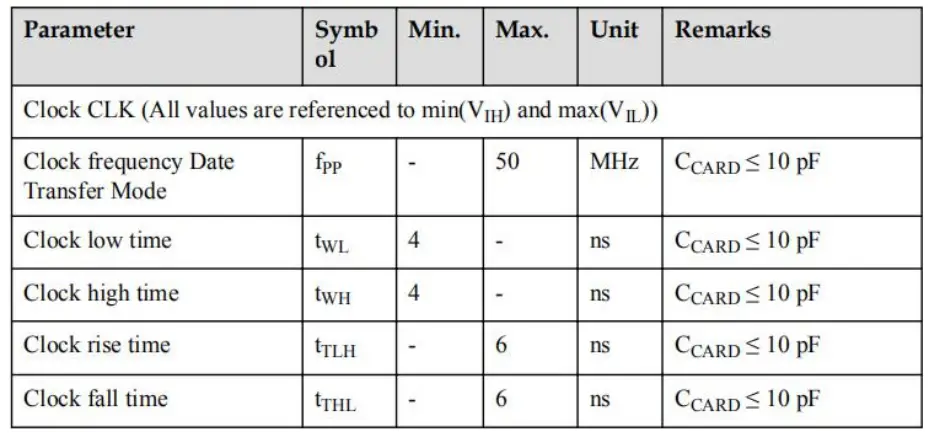
Figure 8-8 shows the input data timing in HS mode. tISU is the setup time, that is, the stability time required by the data of the SDIO interface before clock sampling in this mode. tIH is the hold time, that is, the time required by the data of the SDIO interface to retain the original level after clock sampling in this mode.
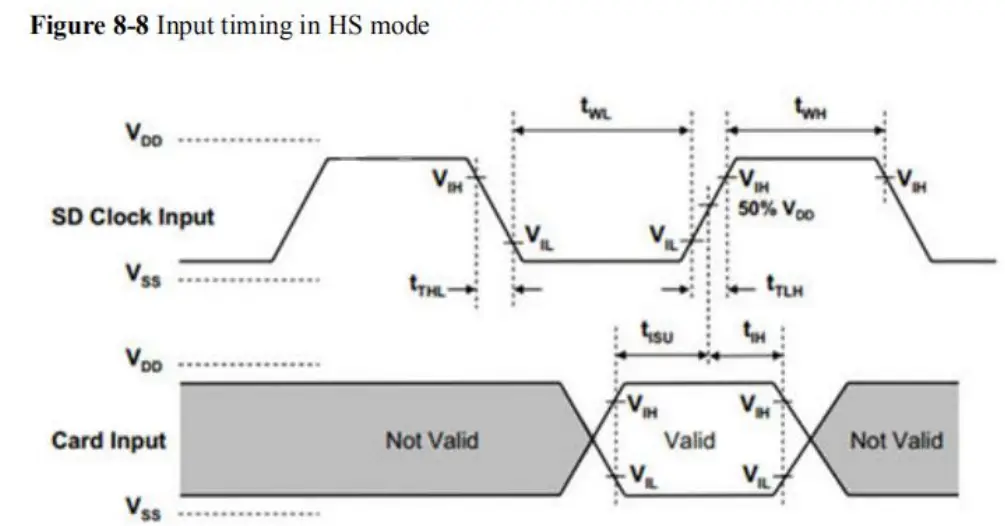
Figure 8-9 shows the input data timing in HS mode. Where, tODLY(max) is the maximum delay of the output data relative to the clock rising edge, and tOH is the minimum delay of the output data relative to the clock rising edge.
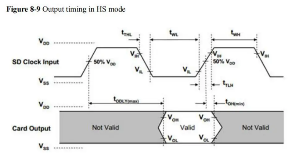
Table 8-15 describes the timing restrictions in HS mode.
Table 8-15 Timing restrictions in HS mode (VDDIO = 3.3 V)
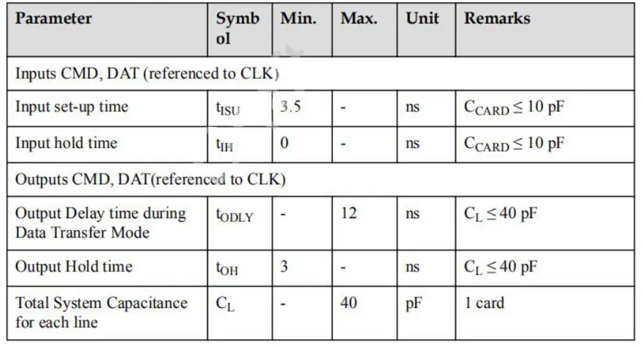
Table 8-16 Timing restrictions in HS mode (VDDIO = 1.8 V)
Note: The data signal timing in HS mode is different from that in DS mode. The output data and input data are referenced to the clock rising edge.
SDR25 Mode
The SDR25 mode is entered only after the voltage of the SDIO is switched. In this mode, the maximum interface clock frequency is 50 MHz. Table 8-17 describes the clock restrictions.
Table 8-17 Clock perameters in SRD25 fnode (VDDIO =3.3 V)
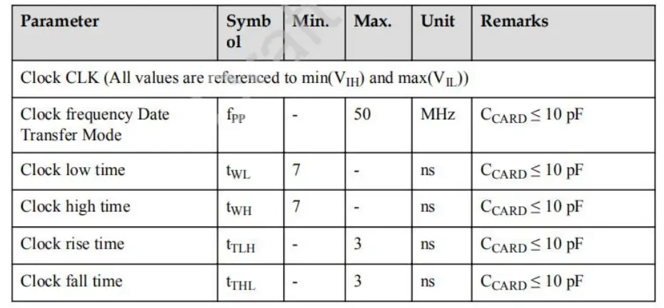
Table 8-18 Clock Perameters in SDR25 mode (VDDIO = 1.8 V)
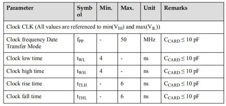
Table 8-19 Timing restrictions in SDR25 mode (VDDIO = 3.3 V)
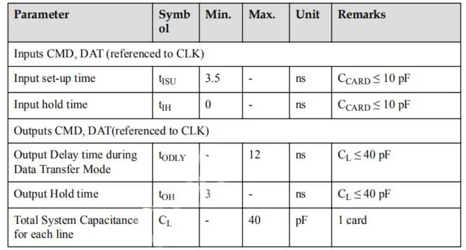
Table 8-19 Timing restrictions in SDR25 mode (VDDIO = 1.8 V)
Reference Design
4line SDIO Reference Design
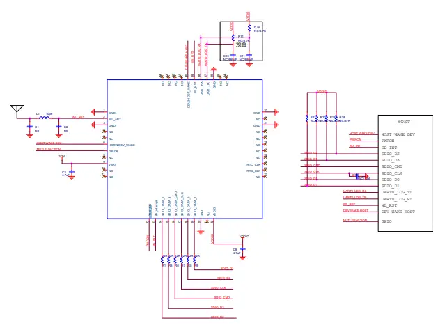
Notes
- 4line WLAN module application, all wake function may not supported;
- Can using Power EN pin to shut down module for power saving;
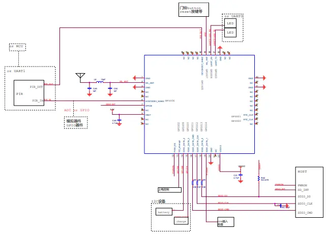
1line SDIO Reference Design
- Hi3861L
GPIO8
GPIO11
GPIO12
GPIO13 - 3161A WIFI
- UART GPIO3/GPIO4
- GPIO3/GPIO5/GPIO7/GPIO14
- GPIO7
- WIFI IO
Ordering Information
| Part No. | Description |
| FG3161ASLX-00 | Hi3861L, b/g/n Wi-Fi, 1T1R, 12X12mm, SDIO, PCB V1.0 Halogen Free,with shielding. |
| FG3161ASLX-01 | Hi3861L, b/g/n Wi-Fi, 1T1R, 12X12mm, SDIO, PCB V1.0 Halogen Free,no shielding. |
The Key Material List
| Main | Inductor | 2016 2.2uH ,±20%,DCR=0.125ohm,Isat=1.5A,Irms=1.5A, MPIE201610-2R2M-LF(麦捷微) | ||||
| Main | Shielding | 3161A-SL-V1.0 | Shielding | cover, no | insulation | glue, no |
| cover | positioning foot (material: copper) Xintai | |
| Main | Crystal | 2520 40MHZ,13.8PF,7ppm,SR:50 Ω ,E2SB40E00000GE (HOSONIC) |
| Alt. | Crystal | 2520 40MHz 15pF ±10ppm -40~85℃ Q40000V024 (东 晶) |
| Main | RTC | 3215 32.768KHZ 12.5PF 20PPM -40~85 ° C SF32K32768D31T-12.5 (泰晶) |
| Main | Chipset | Hi3861LRNIV100 WiFi IoT Soc,802.11b/g/n, WiFi Mesh, 内置 2M Flash, SDIO,UART,支持低功耗,QFN32, 5x5mm (海思) |
Power on Sequence
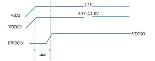
VCC / VDDIO supreme electrical order requirements
In the process of power up, GPIO02 internal weak pull low ,the 40MHz crystal is selected..
Design Attention
- GPIO02 is the interrupt signal of SDIO, It also can be configured as dev wake host function.
- GPIO8 can be setting as SDIO interrupt function.
- PMU_PWRON is enable pin of the module. Default is pull high.
- Wake function may not supported with recently applications, for power saving please using POWER EN pin enable or disable the module.
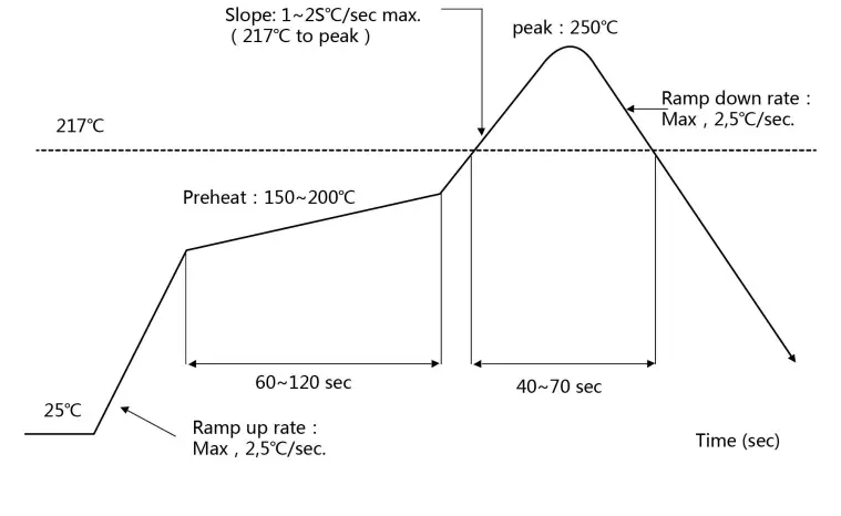
Recommended Reflow Profile
Referred to IPC/JEDEC standard.
Peak Temperature : <250°C
Number of Times : 2 times
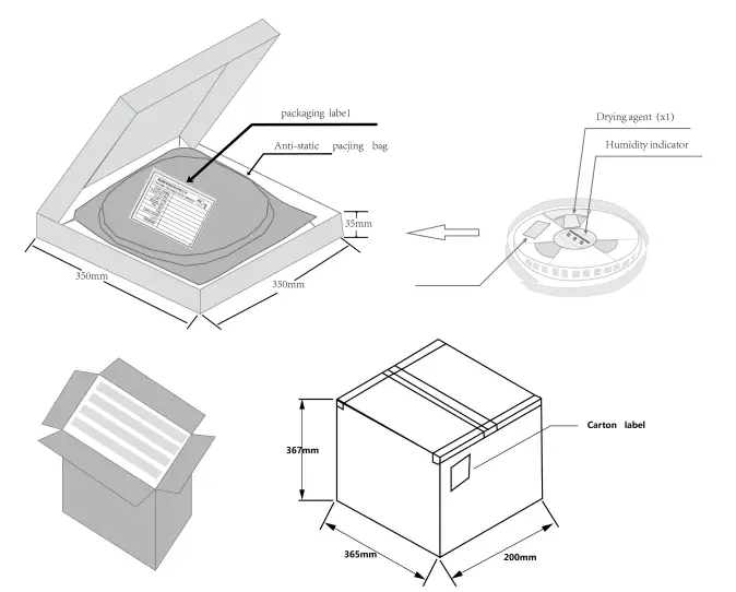
Packing Information
Reel
A roll of 1500pcs
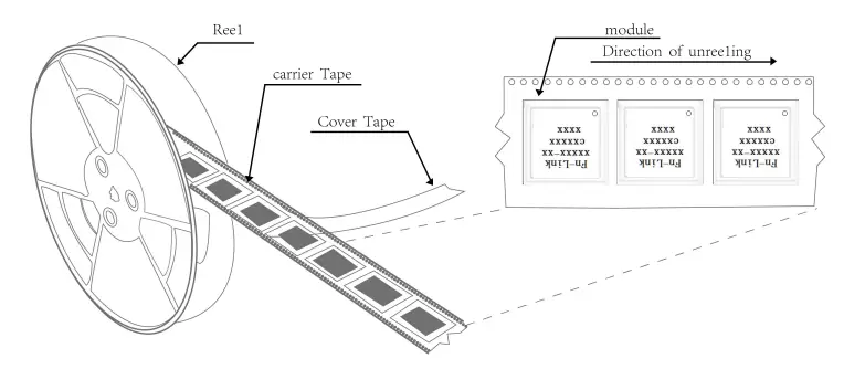
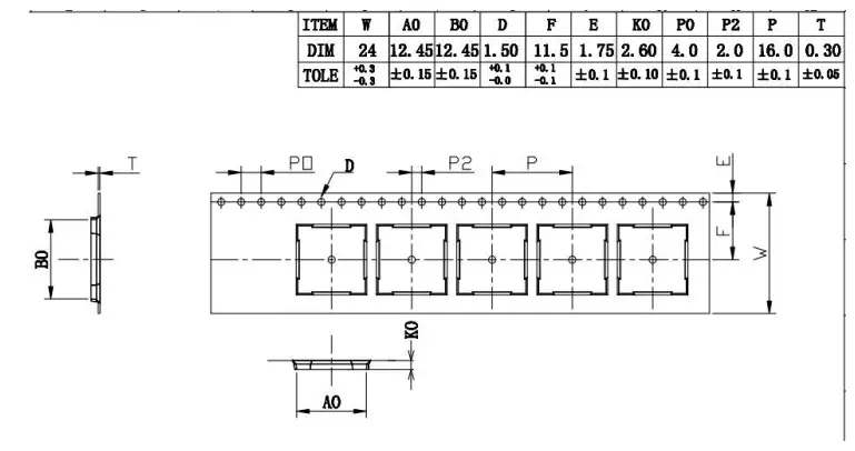
Carrier Tape Detail
Packaging Detail
Moisture sensitivity
The Modules is a Moisture Sensitive Device level 3, in according with standard IPC/JEDEC J-STD-020, take care all the relatives requirements for using this kind of components. Moreover, the customer has to take care of the following conditions:
a) Calculated shelf life in sealed bag: 12 months at <40°C and <90%relativehumidity(RH). b) Environmental condition during the production: 30°C / 60%RH accordingto IPC/JEDEC J-STD-033A paragraph 5. c) The maximum time between the opening of the sealed bag and the reflow process must be 168 hours if condition
b) “IPC/JEDEC J-STD-033A paragraph 5.2” is respected
d) Baking is required if conditions b) or c) are not respected
e) Baking is required if the humidity indicator inside the bag indicates 10%RHor more.
Customer Service
Office: 6 Floor, Building U6, Junxiang U8 Park, Hangcheng Avenue, Bao’an District, Shenzhen City, CHINA
Factory: No.8, Litong Road, Liuyang Economic & Technical
Development Zone, Changsha, Hunan, CHINA
TEL: +86-755-2955-8186
Website: www.fn-link.com
Customer Approval :
Company
Title
Signature
Date
Fn-Link


