M gear BLE Pass-Through Module Bluetooth 5.0
Revision History
| Date | Release | Author | Description |
| 2021/2/5 | R01 | LL/JW | First released |
| 2021/6/23 | R02 | LL/JW | |
| 2021/7/21 | R03 | LL/JW | Add FCC Statement |
Related Documents
| Date | Author | Document(s) |
Overview
BM200 is Bluetooth 5.0 Low Energy serial pass‐through module based on ultra‐low‐power Realtek RTL8762C SOC with built‐in high performance PCB antenna. Just simply connect BM200 module to MCU by using UART interface, focus on MCU firmware development and save time on BLE stack and hardware development, simple and neat.
Feature
- Supports Bluetooth 5.0 Core Specification
- Supports LE_1M, LE_2M, LR2 and LR8
- ARM Cortex‐M4 with floating‐point unit (Maximum 40MHz)
- Total 160KB SRAM
- 4K bits eFuse for manufacturer use
- Embedded 2Mbits flash
- Supports AES128/192/256 encrypt /decrypt engine
- Built‐in PCB antenna
PIN Configurations
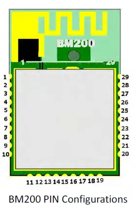
Descriptions of functional PINs
| PIN NO. | PIN NAME | TYPE | DESCRIPTIONS |
| 1 | GND | POWER | GROUND |
| 2 | NRESET | I | Hardware reset pin; low active |
| 3 | P4_3 | IO | General purpose IO; 8mA driving capability. With wakeup function. With internal strong/weak pull‐up and pull‐down. |
| 4 | P4_2 | IO | General purpose IO; 8mA driving capability. With wakeup function. With internal strong/weak pull‐up and pull‐down. |
| 5 | P4_1 | IO | General purpose IO; 8mA driving capability. With wakeup function. With internal strong/weak pull‐up and pull‐down. |
| 6 | P4_0 | IO | General purpose IO; 8mA driving capability. With wakeup function. With internal strong/weak pull‐up and pull‐down. |
| 7 | P0_6 | IO | General purpose IO; 8mA driving capability. With wakeup function. With internal strong/weak pull‐up and pull‐down. |
| 8 | P0_5 | IO | General purpose IO; 8mA driving capability. With wakeup function. With internal strong/weak pull‐up and pull‐down. |
| 9 | VDDIO | POWER | Supply 1.8V~3.3V power for digital IO PAD VDDIO should be less than or equal to VDD |
| 10 | GND | POWER | GROUND |
| 11 | P0_4 | IO | General purpose IO; 8mA driving capability. With wakeup function. With internal strong/weak pull‐up and pull‐down. |
| 12 | P0_3/Power on trap | IO | LOG_UART TX. Power on trap: Pull-up for normal operation Pull-down to bypass executing program code in flash (PAD internal pull-up by default) |
| 13 | P0_2 | IO | General purpose IO; 8mA driving capability. With wakeup function. With internal strong/weak pull‐up and pull‐down. |
| 14 | P0_1 | IO | General purpose IO; 8mA driving capability. With wakeup function. With internal strong/weak pull‐up and pull‐down. |
| 15 | P0_0 | IO | General purpose IO; 8mA driving capability. With wakeup function. With internal strong/weak pull-up and pull-down. |
| 16 | P1_0/SWDIO | IO | General purpose IO; 8mA driving capability. With wakeup function. |
| With internal strong/weak pull-up and pull-down. SWDIO (default). | |||
| 17 | P1_1/SWDCLK | IO | General purpose IO; 8mA driving capability. With wakeup function. With internal strong/weak pull‐up and pull‐down. SWDCLK (default). |
| 18 | GND | POWER | GROUND |
| 19 | VDD | POWER | Supply 1.8V~3.3V power for Module |
| 20 | GND | POWER | GROUND |
| 21 | P3_3 | IO | General purpose IO; 8mA driving capability. With wakeup function. With internal strong/weak pull‐up and pull‐down. |
| 22 | P3_2 | IO | General purpose IO; 8mA driving capability. With wakeup function. With internal strong/weak pull‐up and pull‐down. |
| 23 | P3_1/UART_RX | IO | General purpose IO; 8mA driving capability. With wakeup function. With internal strong/weak pull‐up and pull‐down. HCI_UART_RX (default). |
| 24 | P3_0/UART_TX | IO | General purpose IO; 8mA driving capability. With wakeup function. With internal strong/weak pull‐up and pull‐down. HCI_UART_TX (default). |
| 25 | 32K_XI | A/IO | 32k crystal input or external 32k clock input (optional) Pin share as GPIO when external 32k is not used. |
| 26 | 32K_XO | A/IO | 32k crystal input or external 32k clock input (optional)÷ Pin share as GPIO when external 32k is not used. |
| 27 | P2_2 | IO | General purpose IO; 8mA driving capability. With wakeup function. With internal strong/weak pull‐up and pull‐down. AUXADC input 2. |
| 28 | P2_3 | IO | General purpose IO; 8mA driving capability. With wakeup function. With internal strong/weak pull‐up and pull‐down. AUXADC input 3. |
| 29 | GND | POWER | GROUND |
Electrical Characteristics
| Parameter | Minimum | Typical | Maximum | Units |
| Storage Temperature | ‐55 | +125 | ℃ | |
| Operation Temperature | ‐30 | +80 | ℃ | |
| VDD | 1.8 | 3 | 3.6 | V |
| VDDIO (note: VDDIO ≦VDD) | 1.8 | ‐ | 3.6 | V |
Radio Characteristics
Condition: VDD=3V, VDDIO=3V, ambient temperature=25℃
| Parameter | Minimum | Typical | Maximum | Units |
| Frequency Range | 2402 | ‐ | 2480 | MHz |
| Sensitivity PER≦30.8% (LE2M/LE1M/LR2/LR8) | ‐93/‐96/‐99/‐104 | ‐ | ‐ | dBm |
| Maximum Input level | ‐ | ‐ | ‐1 | dBm |
| Maximum Output Power | 7 | dBm |
Digital IO Pin DC Characteristics
| Parameter | Condition | Min | Typical | Max |
| Input high voltage (V) | VDDIO=3.3V | 2 | 3.3 | 3.6 |
| Input low voltage(V) | VDDIO=3.3V | ‐ | 0 | 0.9 |
| Output hi voltage(V) | VDDIO=3.3V | 2.97 | ‐ | 3.3 |
| Output lo voltage(V) | VDDIO=3.3V | 0 | ‐ | 0.33 |
Power Consumption
Condition: VDD=3V, VDDIO=3V, ambient temperature=25℃
| Power Mode | Always on registers | 32K RCOSC | Retention SRAM | CPU | Wakeup Method | Current Consumption(typ.) |
| Power Down | ON | OFF | OFF | OFF | GPIO | 450nA |
| Deep LPS | ON | ON | Retention | OFF | GPIO,TIMER | 2.5uA |
| Active RX Mode | 7.3mA | |||||
| Active TX Mode | 11.3mA |
Antenna Peak gain & Efficiency
| Frequency (MHz) | Peak Gain (dBi) | Efficiency (%) |
| 2400 | 1.83 | 46 |
| 2450 | 0.37 | 44 |
| 2500 | 0.96 | 43 |
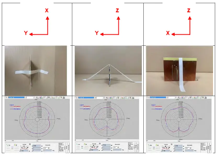
Antenna 2D Radiation Pattern Results
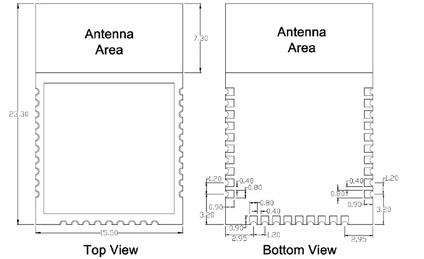
Mechanical Dimensions
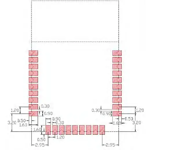
Layout Footprint
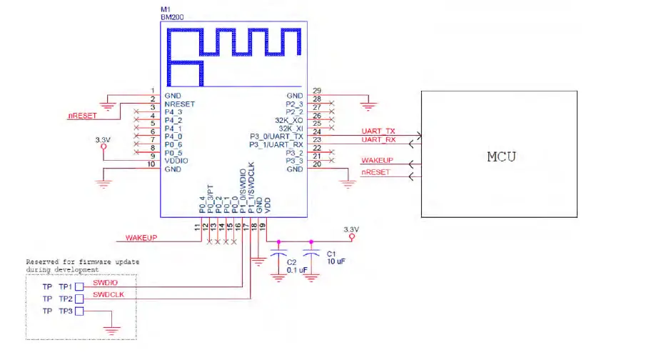
Application Schematic
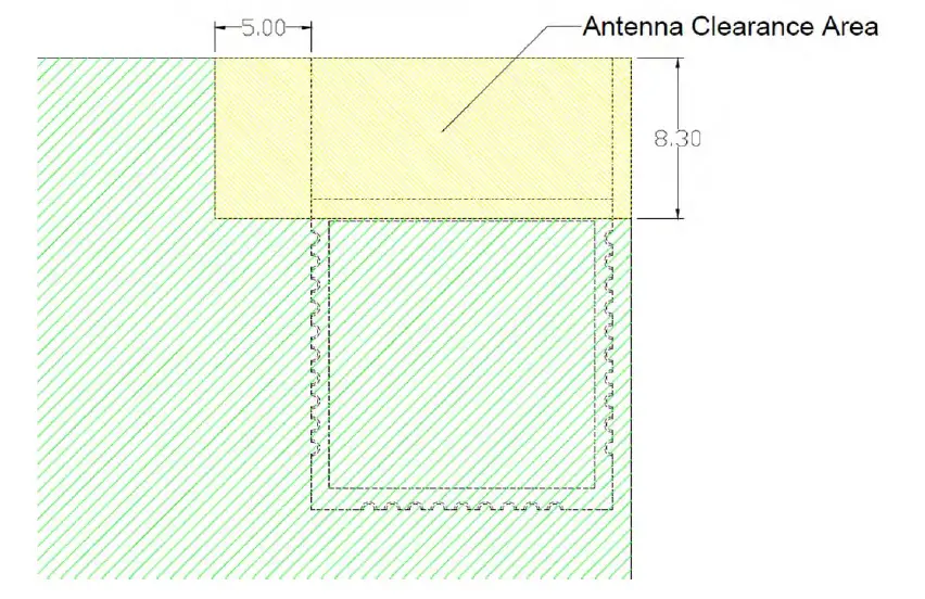
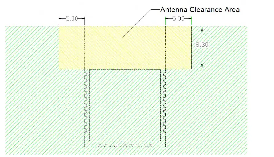
Layout Guideline
Federal Communication Commission Interference Statement
This equipment has been tested and found to comply with the limits for a Class B digital device, pursuant to Part 15 of the FCC Rules. These limits are designed to provide reasonable protection against harmful interference in a residential installation. This equipment generates, uses and can radiate radio frequency energy and, if not installed and used in accordance with the instructions, may cause harmful interference to radio communications. However, there is no guarantee that interference will not occur in a particular installation. If this equipment does cause harmful interference to radio or television reception, which can be determined by turning the equipment off and on, the user is encouraged to try to correct the interference by one of the following measures:
- Reorient or relocate the receiving antenna.
- Increase the separation between the equipment and receiver.
- Connect the equipment into an outlet on a circuit different from that to which the receiver is connected.
- Consult the dealer or an experienced radio/TV technician for help.
FCC Caution: Any changes or modifications not expressly approved by the party responsible for compliance could void the user’s authority to operate this equipment.
This device complies with Part 15 of the FCC Rules. Operation is subject to the following two conditions: (1) This device may not cause harmful interference, and (2) this device must accept any interference received, including interference that may cause undesired operation.
FCC Radiation Exposure Statement:
This equipment complies with FCC radiation exposure limits set forth for an uncontrolled environment. This equipment should be installed and operated with minimum distance 20cm between the radiator & your body.


 Module User Manual")


