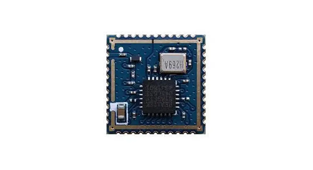
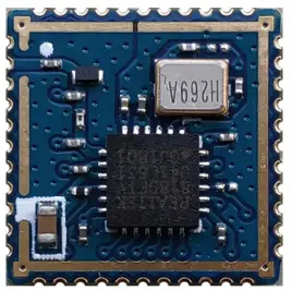
![]() BL-M8189FS6(VC)
BL-M8189FS6(VC)
802.11n 150Mbps WiFi
SDIO Module Specification
| Module Name: BL-M8189FS6(VC) | |
| Module Type: 802.11b/g/n 150Mbps 1T1R WiFi SDIO Module | |
| Revision: V1.0 | |
| Customer Approval: | |
| Company: | |
| Title: | |
| Signature: | Date: |
| BL-link Approval: | |
| Title: | |
| Signature: | Date: |
Revision History
| Revision | Summary | Release Date |
| 1.0 | Official release | 3/25/2020 |
Introduction
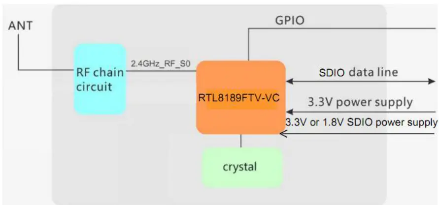
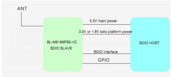
BL-M8189FS6(VC) is a highly integrated WiFi module, it contains a WLAN MAC, a 1T1R capable WLAN baseband. It supports IEEE 802.11b/g/n standard and provides the highest PHY rate up to 150Mbps, offering feature-rich wireless connectivity and reliable throughput from an extended distance.
1.1 Features
- Operating Frequencies: 2.412~2.462GHz
- The host Interface is SDIO 2.0
- IEEE Standards: IEEE 802.11b/g/n
- The wireless data rate can reach up to 150Mbps
- Connect to the external antenna through half hole pad
- Power Supply: 3.3±0.2V main power supply; 3.3±0.2V or 1.8±0.1V for VDIO (SDIO and Digital I/O power supply)
1.2 Block Diagram
1.3 General Specifications
| Module Name | BL-M8189FS6(VC) WiFi Module |
| Chipset | RTL8189FTV-VC-CG |
| WiFi Standards | IEEE802.11b/g/n/, 1T1R, 2.4GHz, 150Mbps (Max) |
| Host Interface | SDIO 3.0 |
| Antenna | Connect to the external antennas through half hole pad |
| Dimension | SMD 44Pins, 12*12*1.5mm (L*W*H) |
| Power Supply | DC 3.3±0.2V(main power) @ 350 mA (Max) DC 3.3±0.2V or 1.8±0.1V(SDIO and Digital I/O power) |
| Operation Temperature | -10℃ to +70℃ |
| Operation Humidity | 10% to 95% RH (Non-Condensing) |
Pin Assignments
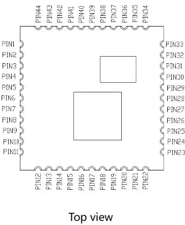 2.1 Pin Definition
| No | Pin Name | Type | Description | Supply |
| 1 | GND | RF | Ground connections | |
| 2 | ANT | RF | WLAN RF port | |
| 3 | GND | RF | Ground connections | |
| 4 | NC | / | NC |
| 5 | NC | / | NC | |
| 6 | NC | / | NC | |
| 7 | NC | / | NC | |
| 8 | NC | / | NC | |
| 9 | VD033 | P | 3.3V Main power supply | |
| 10 | NC | / | NC | |
| 11 | NC | / | NC | |
| 12 | WL_REG_ON | I | Power down select (active low) | VDD33 |
| 13 | WAKE | 0 | WLAN to wake up HOST, pull high for use | VDIO |
| 14 | SD D2 | I/O | SDIO data line | |
| IS | SD D3 | I/O | SDIO data line | |
| 16 | SDCMD | I/O | SDIO command line | |
| 17 | SD_CLK | 1 | SDIO clock line | |
| 18 | SD DO | I/O | SDIO data line | |
| 19 | SD D1 | I/O | SDIO data line | |
| 20 | GND | P | Ground connections | |
| 21 | NC | / | NC | |
| VDIO | P | VIDEO for SDIO and Digital I/O pin, the power supply is | ||
| 22 | same as the signal level of the SDIO bus. Based on a platform to choose 3.3V or 1.8V | |||
| 23 | NC | / | NC | |
| 24 | NC | / | NC | |
| 25 | NC | / | NC | |
| 26 | NC | / | NC | |
| 27 | NC | / | NC | |
| 28 | NC | / | NC | |
| 29 | NC | / | NC | |
| 30 | NC | / | NC | |
| 31 | GND | P | Ground connections | |
| 32 | NC | / | NC | |
| 33 | GND | P | Ground connections | |
| 34 | NC | / | NC | |
| 35 | NC | / | NC | |
| 36 | GND | P | Ground connections | |
| 37 | NC | / | NC | |
| 38 | NC | / | NC |
| 39 | NC | / | NC | |
| 40 | NC | / | NC | |
| 41 | NC | / | NC | |
| 42 | NC | / | NC | |
| 43 | NC | / | NC | |
| 44 | NC | / | NC |
P: Power, I: Input, O: Output, I/O: In/Output, RF: Analog RF Port
Electrical and Thermal Specifications
3.1 Recommended Operating Conditions
| Parameters | Min | Typ | Max | Units | |
| Ambient Operating Temperature | -10 | 25 | 70 | °C | |
| External Antenna VSWR | 1 | 2. | 3. | / | |
| Supply Voltage | VDD33 | 3. | 3. | 4. | V |
| VIDEO(1.8V) | 2. | 2. | 2.0 | V | |
3.2 Current Consumption
| Conditions : VDD33=3.3V ; Ta:25°C | |||
| Use Case | VDD33 Current (average) | ||
| Typ | Max | I Units | |
| WiFi Radio Off (Linux Driver) 40 | 50 mA | ||
| WiFi Unassociated (Linux Driver) 40 | 60 mA | ||
| 2.4G I Mbps TX (RF-Test) | 273 | 320 mA | |
| 2.4G 1Mbps RX (RF-Test) | 60 | 70 | mA |
| 2.4G 1I Mbps TX (RF-Test) | 280 | 320 | mA |
| 2.4G I I Mbps RX (RF-Test) | 55 | 70 | mA |
| 2.4G 6Mbps TX (RF-Test) | 265 | 285 | mA |
| 2.4G 6Mbps RX (RF-Test) | 60 | 70 | mA |
| 2.4G 54Mbps TX (RF-Test) | 260 | 270 | mA |
| 2.4G 54Mbps RX (RF-Test) | 60 | 65 | mA |
| 2.4G MCS0(HT20) TX (RF-Test) | 275 | 287 | mA |
| 2.4G MCS0(HT20) RX (RF-Test) | 60 | 70 | mA |
| 2.4G MCS7(HT20) TX (RF-Test) | 265 | 282 | mA |
| 2.4G MCS7(HT20) RX (RF-Test) | 59 | 70 | mA |
| 2.4G MCS7(HT40) TX (RF-Test) | 275 | 291 | mA |
| 2.4G MCS7(HT40) RX (RF-Test) | 60 | 80 | mA |
Interface Functional and Timing Specifications
4.1 SDIO Power-On Sequence
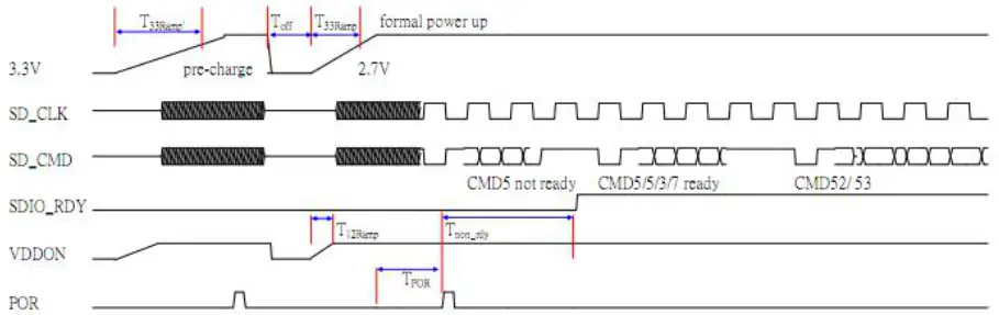
| Min | Typical | Max | Unit | |
| T33rump | 0.2 | 0.5 | 3. | ms |
| Toff | 250 | 500 | 1000 | ms |
| T33ramn | 0.2 | 0.5 | 3. | MS |
| T12ramn | 0.1 | 0.5 | 2. | ms |
| Tpor | 2 | 2 | 8 | ms |
| Upon-rdy | 1 | 2 | 10 | ms |
4.2 SDIO Timing
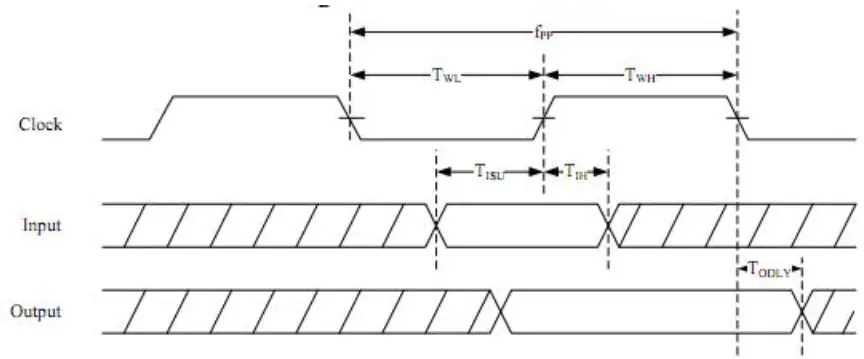
| NO | Parameter | Mode | MIX | MAX | Unit |
| fpp | Clock frequency | default | 0 | 25 | MHz |
| HS | 0 | 50 | MHz | ||
| TwL | Clock low time | DEF | 10 | ns | |
| HS | 7 | ns | |||
| TwL | Clock high time | DEF | 10 | ns |
WiFi RF Specifications
5.1 2.4G WiFi RF Specification
| WLAN Standard | IEEE 802.11b/g/n CSMA/CA |
| Frequency Range | 2.412~2.462GHz (2.4GHz ISM Band) |
| Channels | Ch1~Ch11 (For 20MHz Channels) |
| Modulation | 802.11b (DSSS): DBPSK, DQPSK, CCK; 802.11g (OFDM): BPSK, QPSK, 16QAM, 64QAM; 802.11n (OFDM): BPSK, QPSK, 16QAM, 64QAM; |
| Date Rate | 802.11b: 1, 2, 5.5, 11Mbps; 802.11g: 6, 9, 12, 18, 24, 36, 48, 54Mbps; 802.11n (HT20): MCS0~MCS7(1T1R_SISO) 6.5~72.2Mbps; 802.11n (HT40): MCS0~MCS7(1T1R_SISO) 13.5~150Mbps; |
| Frequency Tolerance | ≦ ±15ppm |
Mechanical Specifications
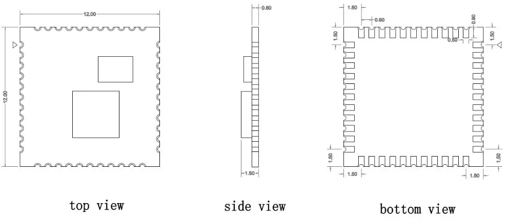
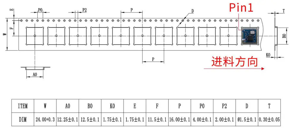
6.1 Module Outline Drawing
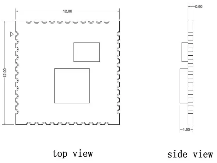
Module dimension: 12.0*12.0*1.5mm (L*W*H; Tolerance: ±0.15mm)
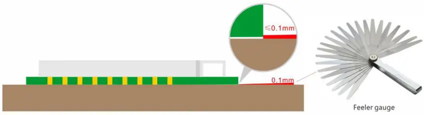
Module Bow and Twist:≤0.1mm
6.2 Mechanical Dimensions
Application Information
7.1 Typical Application Circuit
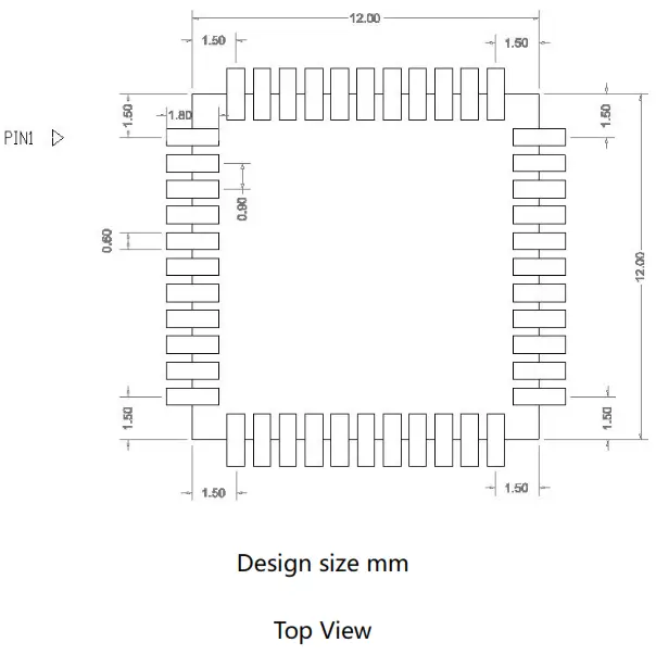
7.2 Recommend PCB Layout Footprint
7.3 Reflow Soldering Standard Conditions
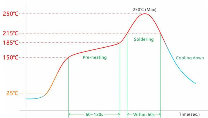
Please use the reflow within 2 times.
Set up the highest temperature within 250℃.
Key Components Of Module
| NO. | Parts | Specification | Manufacturer | Note |
| 1 | Chipset | RTL8189FTV-VC-CG | Realtek | |
| 2 | PCB | BL-M8189FS6 | Shenzhen Tie Fa Technology limited | |
| Guangdong KING SHINE ELECTRONICS CO., LTD | ||||
| Quzhou Sunlord Electronics Co., Ltd | ||||
| 3 | Crystal | 26MHz-9pF-10ppm-3225 | HUBEI TKD ELECTRONICS TECHNOLOGY CO., LTD. | |
| LUCKI CM ELECTRONICS CO., LTD | ||||
| HOSONIC ELECTRONIC CO., LTD. | ||||
| SHENZHEN KAIYUEXIANG ELECTRONICS CO., LTD | ||||
| 4 | TVS diode | TVS diode 0402 | WAY ON ELECTRONIC CO., LTD. | |
| UN Semiconductor Co., Ltd |
Package and Storage Information
9.1 Package Dimensions
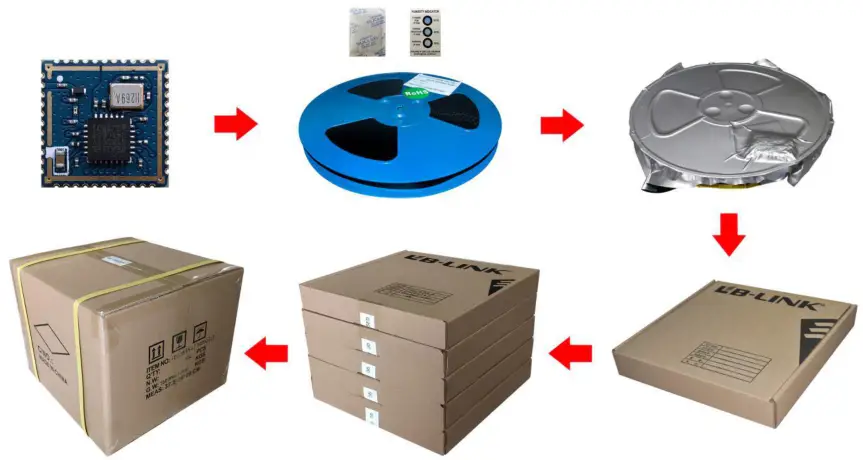
Package specification:
- 2000 modules per roll and 10,000 modules per box.
- Outer box size: 37.5*36*29cm.
- The diameter of the blue environment-friendly rubber plate is 13 inches, with a total thickness of 28mm (with a width of 24mm carrying belt).
- Put 1 package of dry agent (20g) and a humidity card in each anti-static vacuum bag.
- Each carton is packed with 5 boxes.
9.2 Storage Conditions
Absolute Maximum Ratings:
Storage temperature: -45℃ to +85℃
Storage humidity: 10% to 95% RH(Non-Condensing)
Recommended Storage Conditions:
Storage temperature: 5℃ to +40℃
Storage humidity: 20% to 90% RH
Please use this Module within 12 months after being vacuum-packaged.
The Module shall be stored without opening the packing.
After the packing is opened, the Module shall be used within 72hours.
When the color of the humidity indicator in the packing changes, the Module shall be baked before soldering.
Baking condition: 60℃, 24 hours, 1 time.
ESD Sensitivity:
The Module is a static-sensitive electronic device.
Do not operate or store near strong electrostatic fields.
Take proper ESD precautions!
ISED Statement
- English: This device complies with Industry Canada license‐exempt RSS standard(s).
Operation is subject to the following two conditions: (1) This device may not cause interference, a nd (2) This device must accept any interference, including interference that may cause undesired operation of the device.
The digital apparatus complies with Canadian CAN ICES‐3 (B)/NMB‐3(B).
Radiation Exposure Statement
This equipment complies with Canadian radiation exposure limits set forth for an uncontrolled environment. This equipment should be installed and operated with minimum distance 20cm between the radiator & your body.
This device is intended only for OEM integrators under the following condition:
The transmitter module may not be co-located with any other transmitter or antenna.
As long as the condition above is met, further transmitter test will not be required. However, the OEM integrator is still responsible for testing their end-product for any additional compliance requirements required with this module installed.
Important Note:
In the event that these conditions cannot be met (for example certain laptop configurations or co-location with another transmitter), then the Canada authorization is no longer considered valid and the IC cannot be used on the final product. In these circumstances, the OEM integrator will be responsible for re-evaluating the end product (including the transmitter) and obtaining a separate Canada authorization.
Nota Importante:
End Product Labeling The final end product must be labeled in a visible area with the following: Contains IC: 20944M8189FS6.
Manual Information to the End-User
The OEM integrator has to be aware not to provide information to the end-user regarding how to install or remove this RF module in the user’s manual of the end product which integrates this module.
The end-user manual shall include all required regulatory information/warning as shown in this manual.
FCC Statement
This device complies with part 15 of the FCC rules. Operation is subject to the following two conditions: (1) this device may not cause harmful interference, and (2) this device must accept any interference received, including interference that may cause undesired operation. Changes or modifications not expressly approved by the party responsible for compliance could void the user s authority to operate the equipment.
NOTE: This equipment has been tested and found to comply with the limits for a Class B digital device, pursuant to part 15 of the FCC Rules. These limits are designed to provide reasonable protection against harmful interference in a residential installation. This equipment generates uses and can radiate radio frequency energy and, if not installed and used in accordance with the instructions, may cause harmful interference to radio communications. However, there is no guarantee that interference will not occur in a particular installation. If this equipment does cause harmful interference to radio or television reception, which can be determined by turning the equipment off and on, the user is encouraged to try to correct the interference by one or more of the following measures:
- Reorient or relocate the receiving antenna.
- Increase the separation between the equipment and receiver.
- Connect the equipment into an outlet on a circuit different from that to which the receiver is connected.
- Consult the dealer or an experienced radio/TV technician for help with important announcements Important Note:
Radiation Exposure Statement
This equipment complies with FCC radiation exposure limits set forth for an uncontrolled environment. This equipment should be installed and operated with a minimum distance 0cm between the radiator and your body.
This transmitter must not be co-located or operating in conjunction with any other antenna or transmitter. Country Code selection feature to be disabled for products marketed to the US/Canada.
This device is intended only for OEM integrators under the following conditions:
- The antenna must be installed such that 20 cm is maintained between the antenna and users, and
- The transmitter module may not be co-located with any other transmitter or antenna,
- For all products market in the US, OEM has to limit the operation channels in CH1 to CH11 for 2.4G band by supplied firmware programming tool. OEM shall not supply any tool or info to the end-user regarding Regulatory Domain change. (if modular only test Channel 1-11)
As long as the three conditions above are met, further transmitter testing will not be required. However, the OEM integrator is still responsible for testing their end-product for any additional compliance requirements required with this module installed.
Important Note:
In the event that these conditions cannot be met (for example certain laptop configurations or co-location with another transmitter), then the FCC authorization is no longer considered valid and the FCC ID cannot be used on the final product. In these circumstances, the OEM integrator will be responsible for re-evaluating the end product (including the transmitter) and obtaining a separate FCC authorization.
End Product Labeling
The final end product must be labeled in a visible area with the following” Contains FCC ID: 2AL6KBLM8189FS6″
Manual Information to the End-User
The OEM integrator has to be aware not to provide information to the end-user regarding how to install or remove this RF module in the user’s manual of the end product which integrates this module.
The end-user manual shall include all required regulatory information/warning as shown in this manual.
Integration instructions for host product manufacturers according to KDB 996369 D03 OEM Manual v01
2.2 List of applicable FCC rules
CFR 47 FCC PART 15 SUBPART C has been investigated. It is applicable to the modular transmitter
2.3 Specific operational use conditions
This module is stand-alone modular. If the end product will involve the Multiple simultaneously transmitting condition or different operational conditions for a stand-alone modular transmitter in a host, the host manufacturer has to consult with the module manufacturer for the installation method in the end system.
2.4 Limited module procedures
This module is a Limited single modular without shielding, host manufacturer has to consult with the module manufacturer for the module limiting conditions when integrating the module into the host. module manufacturer should review detailed test data or host designs prior to giving the host manufacturer approval.
2.5 Trace antenna designs
Not applicable
2.6 RF exposure considerations
This equipment complies with FCC radiation exposure limits set forth for an uncontrolled environment. This equipment should be installed and operated with a minimum distance of 20cm between the radiator & your body.
2.7 Antennas
This radio transmitter 2AL6KBL-M8189FS6 has been approved by Federal Communications Commission to operate with the antenna types listed below, with the maximum permissible gain indicated. Antenna types not included in this list that have a gain greater than the maximum gain indicated for any type listed are strictly prohibited from use with this device.
| Peak gain ( dBi ) | |||||||
| Model | Type | connector | 2400-2483.5 | 5150-5250 | 5250-5350MHz | 5470-5725 | 5725-5850 |
| MHz | MHz | MHz | MHz | MHz | |||
| 2400-2483.5 MHz | External Antenna | / | 2.0dBi | / | / | / | / |
2.8 Label and compliance information
The final end product must be labeled in a visible area with the following” Contains FCC ID:2AL6KBL-M8189FS6″.
2.9 Information on test modes and additional testing requirements
The host manufacturer which installs this modular with limited modular approval should perform the test of radiated emission and spurious emission according to FCC part 15C:15.247 and 15.209 requirements, only if the test result complies with FCC part 15.247 and 15.209 requirements, then the host can be sold legally.
2.10 Additional testing, Part 15 Subpart B disclaimer
The host manufacturer is responsible for compliance of the host system with the module installed with all other applicable requirements for the system such as Part 15 B.


