AUVIDEA JN30D Carrier Board for NVIDIA Jetson Nano
Document revisions and changes
| Document version | Changes |
| 1.0 | Initial document, internal verification process |
| 1.1 | Internal verification process |
| 1.2 | Updated contents, new pictures |
Product revisions and changes
| Product version | Changes |
| 38488 | Engineering prototype |
| 38488 | Production release |
Overview
Jetson compute module
This new JN30D carrier board has been designed primarily for the Jetson Nano compute modules. When using other modules like the Jetson NX power limits may be exceeded as the USB C power supply only supplies up to 3A. More power may be supplied to the board via the two 5V pins on the GPIO header. In this case the USB supply should not be connected.
JN30D
- Easy integration into passively cooled systems
- Optionally available as a complete system in a passively cooled enclosure
- Easy flashing: just connect a USB OTG cable (Auto Flash)
- High-performance storage: M.2 NVME PCIe x4
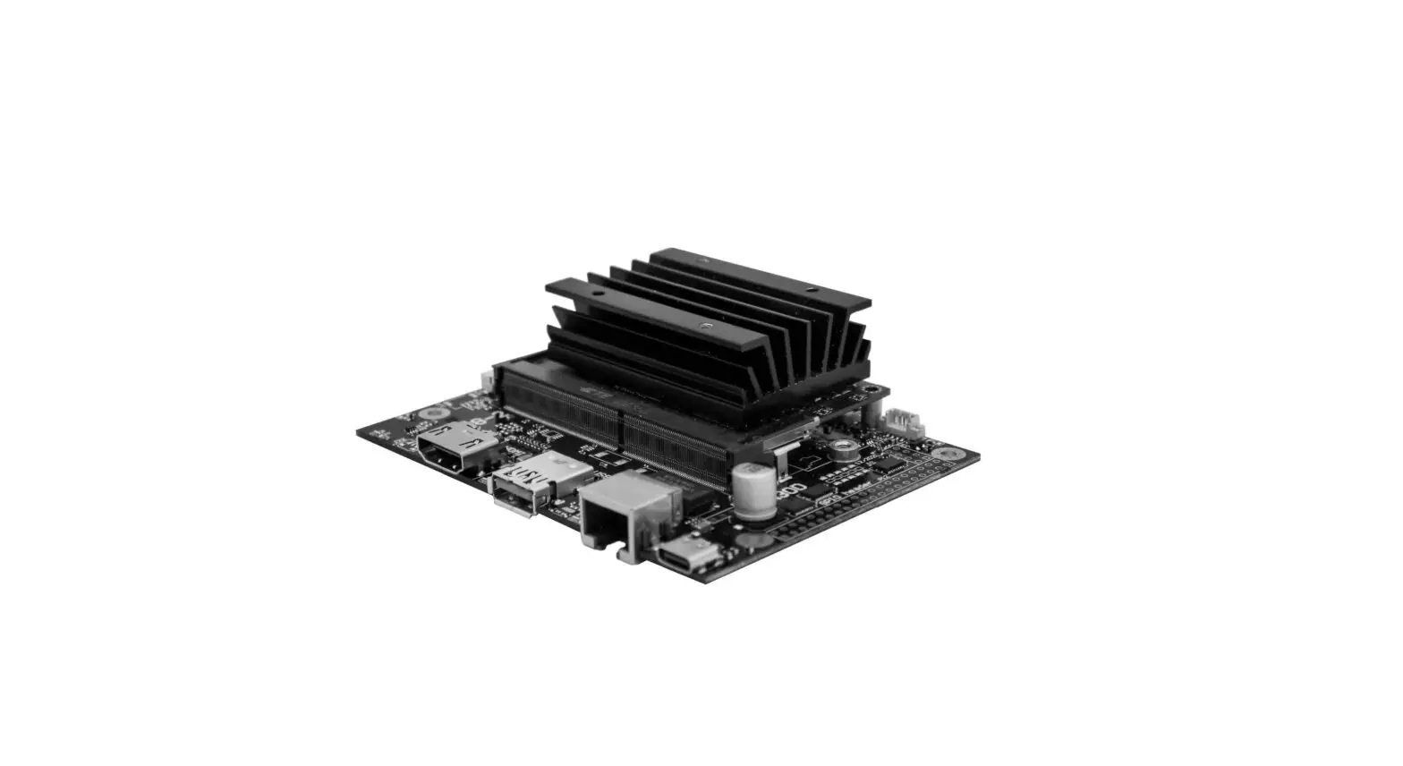
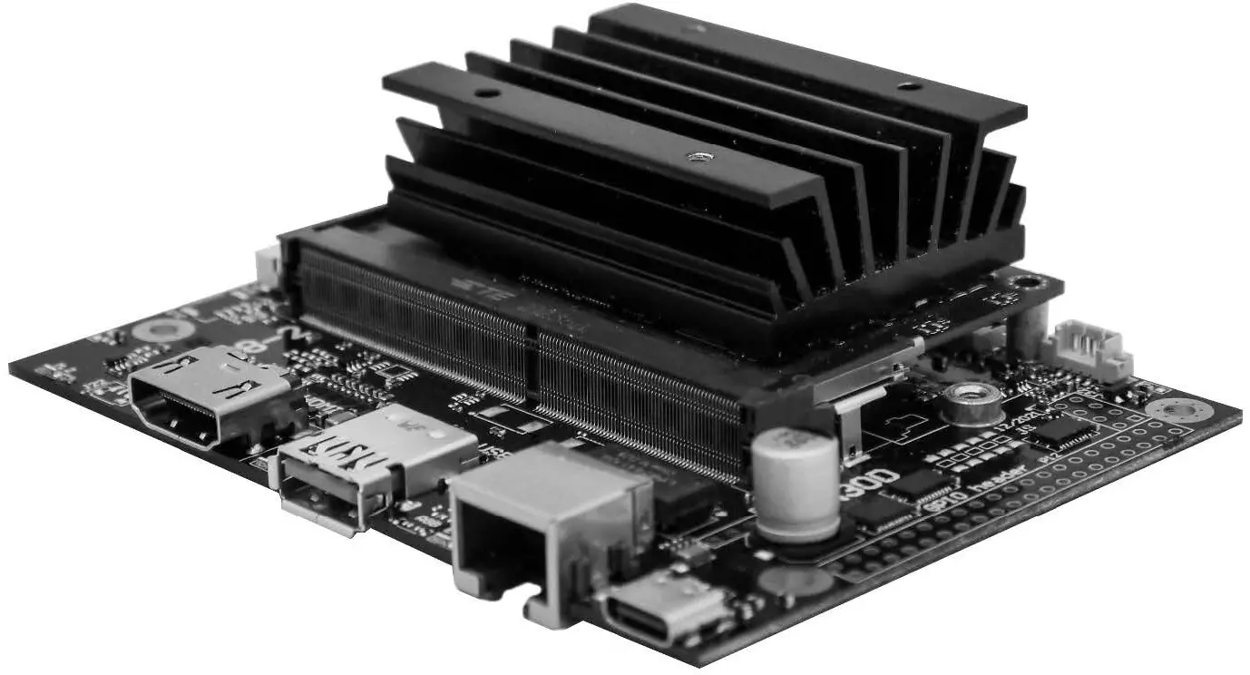
Model pictures
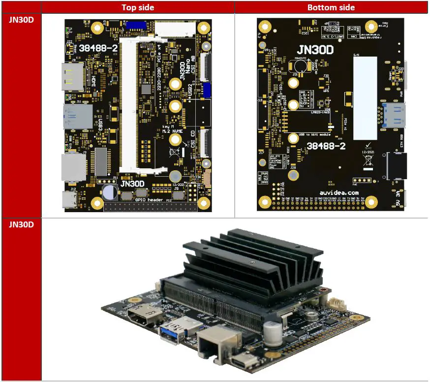
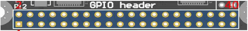
The 40-pin GPIO header is included (but not soldered in).
JN30D features and comparison
| Description | JN30D | NVIDIA Devkit |
| Power | 6V – 19V (5.5/2.5mm connector) | 5V – 19V |
| NX powering | 5V 8A power supply | ? |
| DP | no | yes |
| HDMI | yes | yes |
| Fan connector | yes | yes |
| M.2 NVME Key M | yes | yes |
| Micro SD card | no (optional) | no |
| M.2 Key E | only with external module (using internal USB – J8) | yes |
| CAN RX / TX | no (optional) | yes |
| USB 3.0 | 1x USB 3.1 (native – full performance) | 4x USB 3.1 (via USB hub – shared) |
| Micro USB | 1x Micro USB (host and device mode) | 1x Micro USB (device mode only) |
| Auto Flashing | yes (plug in host cable and flash) | no |
| USB 2.0 | 1x USB 2.0 (JST-GH, J8) | no |
| Ethernet | Gigabit RJ45 (one LED) | Gigabit RJ45 (2 LEDs) |
| PoE option | yes – P11 | yes |
| CSI | 2x CSI-2 (4 lanes) plus camera LED (hardware sync available) | 2x CSI-2 |
| UART | 2x (J14 and 40 pin GPIO header) | 2x (40 pin header) |
| I2C | 2x (40 pin header) | 2x (40 pin header) |
| I2S | 1x (40 pin header) (5V tolerant, unidirectional) | 1x (40 pin header) |
| SPI | 2x (40 pin header) (5V tolerant, unidirectional) | 2x (40 pin header) |
| GPIO | 3x in + 3x out (40 pin header) (5V tolerant, unidirectional) | 6x bi dir (40 pin header) |
| Additional features | ||
| Protection | overvoltage protection (TVS diode) | ? |
| Level shifters | unidirectional level shifters (work better) | bi dir (can cause problems) |
| Expandability | 1. Fully populated variants available | no |
| 2. Add-on boards for more USB and Ethernet | ||
| 3. IMU | ||
| 4. board EEPROM and crypto chip (for SW copy protection) | ||
| 5. PCIe x1 connector | ||
| 6. LM823 WIFI module | ||
| 7. 2 more CSI-2 interfaces (2 lanes each) | ||
| 8. RTC battery (rechargeable) | ||
| 9. Over current fuse (product safety) | ||
| 10. UPS option for graceful power down | ||
| 11. On board MCU for watchdog and remote power cycle (LTE) |
Technical specifications
| Description | Note |
| HDMI | standard HDMI connector (2.0) |
| USB 3 | 5Gb/s or 10Gb/s |
| Physical size | 80x 104.6mm |
| Mounting holes | 4x M3 |
| Temperature range | 0 to 70°C (extended range optional) |
| Humidity | noncondensing |
| Longevity | no temperature-sensitive components (like electrolytic capacitors) |
Power consumption
| Description | JN30D |
| Carrier board logic | < 1 watt |
| 3.3V power converter efficiency | > 90% |
Options
- Flexible design and manufacturing
- designed and manufactured in Germany
- in-house fully automated production line with 3D AOI
- special configuration possible with minimum purchase quantity (display port, M.2, PoE, 48V power in, super cap option, 2 RPi camera module connectors, SPI, I2C, switches, etc.)
- design services: you architect your custom carrier board and Auvidea designs and produces it
- please ask for a quote
Features
GPIO-Header
A 40-pin 2.54mm header for GPIO, I2C, I2S and UART. Die pinout is similar to the GPIO header on the NVIDIA dev kits and on the Raspberry Pi. Please note that all signals (except I2C) have uni-directional level shifters. In other boards, some of these signals may be bi-directional which may cause compatibility issues. Auvidea does not guarantee compatibility to any specific add-on boards. Please check the compatibility yourself. Some signals are 5V tolerant inputs and therefore may be driven from 5V logic outputs.
The 40 pin GPIO header is included (but not soldered in).
Crypto chip
The crypto chip has been added to support software licensing and copy protection. Please check the datasheet of the manufacturer for details.
Model: ATSHA204A-MAHCZ-T
https://ww1.microchip.com/downloads/en/DeviceDoc/ATSHA204A-Data-Sheet-40002025A.pdf
MCU
An MCU for additional power management and watchdog functions is optional. It is standard on some of the extended versions of the JN30D.
Pinout description
Please note that the software GPIO number differs from the socket pin number. This software GPIO number must be computed with a special formula and differs between the various compute modules. Please see appendix B for details.
J3 – Ethernet (GbE)
Standard RJ45 pinout with PoE capable magnetics class 3 and 4 (PD or PSE). Connected to the Ethernet controller on the compute module.
J4 – M.2 PCIEx4 NVME SSDs
Please note that only NVME SSDs are supported. SATA SSDs are not supported. We recommend the 128GB Transcend SSDs (TS128GMTE110S). This SSD is standard in some of the Auvidea development system offerings.
J5 – CSI-2 CD
22 pin 0.5mm pitch FPC connector
| Pin | Description | Socket pin | Note |
| 1 | 3.3V | Power: connected with bead to 3.3V (5V optional if bead is moved) | |
| 2 | GEN1_I2C_SDA | 187 | |
| 3 | GEN1_I2C_SCL | 185 | |
| 4 | GND | ||
| 5 | CAM2-MCLK | IN: Input – connect to 1.8V or 3.3V output of the camera to drive the CAM LED. 1: enable CAM LED 0: disable CAM LED | |
| 6 | CAM2_PWDN | 206 | OUT: Output (open drain with 2.2k pullup to 3.3V) – connect to power enable of camera. The control signal is connected via level shifting inverter to pin 152 of the compute module. |
| 7 | GND | ||
| 8 | CSI_D_D1_P | 66 | |
| 9 | CSI_D_D1_N | 64 | |
| 10 | GND | ||
| 11 | CSI_D_D0_P | 42 | |
| 12 | CSI_D_D0_N | 40 | |
| 13 | GND | ||
| 14 | CSI_C_CLK_P | 54 | |
| 15 | CSI_C_CLK_N | 52 | |
| 16 | GND | ||
| 17 | CSI_C_D1_P | 60 | |
| 18 | CSI_C_D1_N | 58 | |
| 19 | GND |
| 20 | CSI_C_D0_P | 48 |
| 21 | CSI_C_D0_N | 46 |
| 22 | GND |
J8 – USB 2.0
JST-GH 1.25mm
| Pin | Description | Socket pin | Note |
| 1 | 5V | ||
| 2 | USB2_D_N | 121 | |
| 3 | USB2_D_P | 123 | |
| 4 | GND |
Internal USB 2.0 JST-GH connector to connect to internal USB 2.0 add-on modules (like U100, U110, U120, etc).
J9 – HDMI
Standard pinout
CEC is not supported (pin 13 of HDMI connector) Power pin 18 is current limited by PTC fuse (5V 50mA)
J10 – CSI-2 AB
22 pin 0.5mm pitch FPC connector
| Pin | Description | Socket pin | Note |
| 1 | 3.3V | Power: connected with bead to 3.3V (5V optional if bead is moved) | |
| 2 | CAM-I2C_SDA | 215 | |
| 3 | CAM-I2C_SCL | 213 | |
| 4 | GND |
| 5 | CAM1-MCLK | IN: Input – connect to 1.8V or 3.3V output of the camera to drive the CAM LED. 1: enable CAM LED 0: disable CAM LED | |
| 6 | CAM1_PWDN | 206 | OUT: Output (open drain with 2.2k pullup to 3.3V) – connect to power enable of camera. The control signal is connected via level shifting inverter to pin 152 of the compute module. |
| 7 | GND | ||
| 8 | CSI_B_D1_P | 17 | |
| 9 | CSI_B_D1_N | 15 | |
| 10 | GND | ||
| 11 | CSI_B_D0_P | 5 | |
| 12 | CSI_B_D0_N | 3 | |
| 13 | GND | ||
| 14 | CSI_A_CLK_P | 12 | |
| 15 | CSI_A_CLK_N | 10 | |
| 16 | GND | ||
| 17 | CSI_A_D1_P | 18 | |
| 18 | CSI_A_D1_N | 16 | |
| 19 | GND | ||
| 20 | CSI_A_D0_P | 6 | |
| 21 | CSI_A_D0_N | 4 | |
| 22 | GND |
See further details in the J5 description.
J11 – USB 3.0 – 3.1
- USB 3.0 Type A standard pinout
- In Rev 1: power control is always on (5V 1A)
- In Rev 2 and up: Controllable with GPIO pin 126 power on[0]/off[1] (default on[0]) (5V 1A)
J12 – USB-C
- Main power input to the carrier board with the 5V 3A USB C power supply.
- Connected with USB 2.0 speed (USB0 bus of the compute module
- Supports device mode and can be used to flash the compute module.
- No overcurrent and no reverse voltage protection were implemented. Power is limited by the USB power supply.
- Alternative 5V powering via the two 5V pins of the GPIO header.
J14 – UART connector
JST-GH 1.25mm
| Pin | Description | Socket pin | Note |
| 1 | 5V |
| 2 | UART0_TXD | 99 | OUT (3.3V) |
| 3 | UART0_RXD | 101 | IN (3.3V) |
| 4 | UART2_TXD | 236 | OUT, Debug port (3.3V) |
| 5 | UART2_RXD | 238 | IN, Debug port (3.3V) |
| 6 | GND |
Unidirectional directional 1.8V to 3.3V level shifters and 10 Ohm series resistance (plus ESD protection).
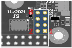
J32 – Button and LED header
| Pin | Description | Socket pin | Note |
| 1 | CAM_LED | 218 | OUT: open drain (3.3V to 12V) |
| 2 | 5V | Connection to internal power rail (PoE power injection possible with optional PoE module). No reverse power protection, this could back power J12 USB-C connector | |
| 3 | BTN PWR ON | – | default: auto power on, no function in rev 1 |
| 4 | VDD RTC | 235 | real time clock battery |
| 5 | SYS RST IN | 239 | IN, open drain (1.8V) |
| 6 | GPIO_PA6 | 178 | IN/OUT, no level shifter (1.8V) |
| 7 | Force recovery | 214 | IN: open drain (1.8V) |
| 8 | GND |
CAM_LED: open drain output to drive the cathode of the camera LED.
Controlled by 3 signals which are OR ‘red together:
- J5 pin 5 (CSI CD camera)
- J10 pin 5 (CSI AB camera)
- Compute module GPIO_12: pin 218 (0: LED off, 1: LED on, float: LED on)
CAM_LED flash signal can be used to control the external camera LED. When using external LED please limit currently with an external resistor. Connect the cathode to this pin and anode to 3.3V to 12V power. Maximum current 2A.
J36 – Fan connector
Pico blade 1.5mm
| Pin | Description | Socket pin | Note |
| 1 | GND | ||
| 2 | 5V | max. 1A | |
| 3 | TACH | – | not connected |
| 4 | PWM | 230 |
P11 – PoE connector
This connects to the 4 center pins of the ethernet magnetics on the cable side to extract or inject PoE power. This connector may be used for PoE addon solutions.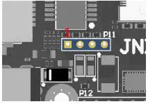
P12 – GPIO header
| Pin | Description | Socket pin | Note |
| 1 | 3.3V | ||
| 2 | 5V | alternative power supply input | |
| 3 | I2C1_SDA | 189 | GEN2_I2C_SDA (3.3V) |
| 4 | 5V | alternative power supply input | |
| 5 | I2C1_SCL | 189 | GEN2_I2C_SCL (3.3V) |
| 6 | GND | ||
| 7 | GPIO09_LS | 211 | OUT (3.3V) |
| 8 | UART1_TXD_LS | 203 | OUT (3.3V) |
| 9 | GND | ||
| 10 | UART1_RXD_LS | 205 | IN (3.3V, 5V tolerant) |
| 11 | UART1_RTS_LS | 207 | OUT (3.3V) |
| 12 | I2S0_SCLK_LS | 199 | OUT (3.3V) |
| 13 | SPI1_SCK_LS | 106 | OUT (3.3V) |
| 14 | GND | ||
| 15 | GPIO12_LS | 218 | OUT (3.3V) |
| 16 | SPI1_CS1_LS | 112 | OUT (3.3V) |
| 17 | 3.3V | ||
| 18 | SPI1_CS0_LS | 110 | OUT (3.3V) |
| 19 | SPI0_MOSI_LS | 89 | OUT (3.3V) |
| 20 | GND | ||
| 21 | SPI0_MISO_LS | 93 | IN (3.3V, 5V tolerant) |
| 22 | SPI1_MISO_LS | 108 | IN (3.3V, 5V tolerant) |
| 23 | SPI0_SCK_LS | 91 | IN (3.3V, 5V tolerant) |
| 24 | SPI0_CS0_LS | 95 | OUT (3.3V) |
| 25 | GND | ||
| 26 | SPI0_CS1_LS | 97 | OUT (3.3V) |
| 27 | ID_I2C_SDA | 187 | GEN1_I2C_SDA (3.3V) |
| 28 | ID_I2C_SCL | 185 | GEN1_I2C_SCL (3.3V) |
| 29 | GPIO01_LS | 118 | IN (3.3V, 5V tolerant) |
| 30 | GND | ||
| 31 | GPIO11_LS | 216 | IN (3.3V, 5V tolerant) |
| 32 | GIIO07_LS | 206 | OUT (3.3V) |
| 33 | GPIO13_LS | 228 | IN (3.3V, 5V tolerant) |
| 34 | GND | ||
| 35 | I2S0_LRCK_LS | 197 | OUT (3.3V) |
| 36 | UART1_CTS_LS | 209 | IN (3.3V, 5V tolerant) |
| 37 | SPI1_MOSI_LS | 197 | OUT (3.3V) |
| 38 | I2S0_SDIN_LS | 195 | IN (3.3V, 5V tolerant) |
| 39 | GND | ||
| 40 | I2S0_SDOUT_LS | 193 | OUT (3.3V) |
Please use any Raspberry Pi hats with care and carefully check compatibility as compatibility was in mind but cannot be guaranteed for all modules.
All GPIO signals are unidirectional (input or output).
U10 – Crypto chip
- Model: ATSHA204A
| Pin | Description | Socket pin | Note |
| 1 | NC | ||
| 2 | NC | ||
| 3 | NC | ||
| 4 | GND | ||
| 5 | GEN3_I2C_SDA | ||
| 6 | GEN3_I2C_SCL | ||
| 7 | NC | ||
| 8 | 3.3V |
Integrated for software protection and licensing.
Datasheet Link:
https://ww1.microchip.com/downloads/en/DeviceDoc/ATSHA204A-Data-Sheet-40002025A.pdf.
LED – M.2
Shows M.2 activity.
LED – Eth
Shows Ethernet activity on Socket pin 194 – on[0]/off[1], default: off At own risk resistor can be moved to control Eth-LED via socket pin 188 (link LED)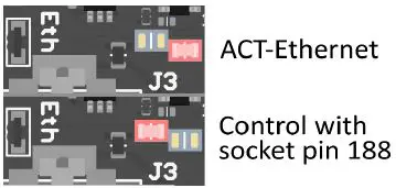
LED – PWR
Connected to 3.3V power rail. This LED is always on when 3.3V is present on the power rail.
Disclaimer
- Thank you for reading this manual. If you have found any typos or errors in this document, please let us know.
- This is the preliminary version of this data sheet. Please treat all specifications with caution as there may be any typos or errors.
- The Auvidea Team
Copyright notice
Trademarks
NVIDIA, the NVIDIA logo, CUDA, Jetson, Maxwell, Tegra, Nano and VisionWorks are registered trademarks and/or trademarks of NVIDIA Corporation in the United States and other countries. Other company and product names may be trademarks of the respective companies with which they are associated.
© Auvidea GmbH 2021
All Rights Reserved
No part of this document or any of its contents may be reproduced, copied, modified or adapted, without the prior written consent of the author, unless otherwise indicated for stand-alone materials.
You may share this document by any of the following means: this PDF file may be distributed freely if no changes or modifications to the document are made. For any other mode of sharing, please contact the author at the email below. [email protected] Commercial use and distribution of the contents of this document is not allowed without express and prior written consent of Auvidea GmbH.
Appendix
Appendix A [CSI-Cameras]
Camera connection example
CSI cameras can connect to J5-CSI-2-CD and J19–CSI-2-AB connectors as shown below.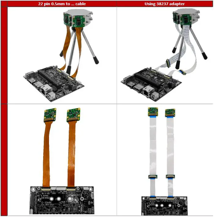
Appendix B [GPIO]
GPIO control
This example shows how to set and read out GPIO 414. For different GPIO numbers replace 414 accordingly.
Export GPIO
- nvidia@nvidia-desktop:~$ echo 414 > /sys/class/gpio/export
- nvidia@nvidia-desktop:~$
Change direction to in
- nvidia@nvidia-desktop:~$ echo in > /sys/class/gpio/gpio414/direction
- nvidia@nvidia-desktop:~$
Change direction to out
- nvidia@nvidia-desktop:~$ echo out > /sys/class/gpio/gpio414/direction
- nvidia@nvidia-desktop:~$
Set GPIO low
- nvidia@nvidia-desktop:~$ echo 0 > /sys/class/gpio/gpio414/value
- nvidia@nvidia-desktop:~$
Set GPIO high
- nvidia@nvidia-desktop:~$ echo 1 > /sys/class/gpio/gpio414/value
- nvidia@nvidia-desktop:~$
Readout GPIO value
- nvidia@nvidia-desktop:~$ cat /sys/class/gpio/gpio414/value
0 - nvidia@nvidia-desktop:~$ cat /sys/class/gpio/gpio414/value
1
Pin to GPIO reference sheet for Xavier-NX/Nano/TX2-NX
| Pin number (Socket number) | Xavier NX GPIOname | Xavier NX GPIOnumber | Xavier NX Pin direction | Nano GPIOname | Nano GPIOnumber | Nano Pin direction | TX2 NX GPIOname | TX2 NX GPIOnumber | TX2 NX Pin direction |
| 1 | |||||||||
| 87 | GPIO3_PZ.01 | 489 | Bidirectional | GPIO3_PCC.04 | 228 | Bidirectional | GPIO3_PL.04 | 412 | Bidirectional |
| 88 | GPIO3_PM.00 | 384 | Input | GPIO3_PCC.06 | 230 | Input | GPIO3_PP.00 | 440 | Input |
| 89 | GPIO3_PZ.05 | 493 | Not Assigned | GPIO3_PC.00 | 16 | Input | GPIO3_PH.02 | 378 | Input |
| 91 | GPIO3_PZ.03 | 491 | Not Assigned | GPIO3_PC.02 | 18 | Input | GPIO3_PH.00 | 376 | Input |
| 93 | GPIO3_PZ.04 | 492 | Not Assigned | GPIO3_PC.01 | 17 | Input | GPIO3_PH.01 | 377 | Input |
| 94 | GPIO3_PM.04 | 388 | Bidirectional | GPIO3_PCC.00 | 224 | Bidirectional | GPIO3_PP.02 | 442 | Bidirectional |
| 95 | GPIO3_PZ.06 | 494 | Not Assigned | GPIO3_PC.03 | 19 | Input | GPIO3_PH.03 | 379 | Input |
| 96 | GPIO3_PM.01 | 385 | Input | GPIO3_PCC.01 | 225 | Input | GPIO3_PP.01 | 441 | Input |
| 97 | GPIO3_PZ.07 | 495 | Not Assigned | GPIO3_PC.04 | 20 | Input | GPIO3_PY.03 | 515 | Input |
| 99 | GPIO3_PX.04 | 476 | Output | GPIO3_PD.01 | 25 | Output | GPIO3_PX.00 | 504 | Output |
| 101 | GPIO3_PX.05 | 477 | Input | GPIO3_PD.02 | 26 | Input | GPIO3_PX.01 | 505 | Input |
| 103 | GPIO3_PX.06 | 478 | Output | GPIO3_PD.03 | 27 | Output | GPIO3_PX.02 | 506 | Output |
| 104 | GPIO3_PY.02 | 482 | Not Assigned | GPIO3_PB.04 | 12 | Input | GPIO3_PV.03 | 491 | Input |
| 105 | GPIO3_PX.07 | 479 | Input | GPIO3_PD.04 | 28 | Input | GPIO3_PX.03 | 507 | Input |
| 106 | GPIO3_PY.00 | 480 | Not Assigned | GPIO3_PB.06 | 14 | Input | GPIO3_PV.01 | 489 | Input |
| 108 | GPIO3_PY.01 | 481 | Not Assigned | GPIO3_PB.05 | 13 | Input | GPIO3_PV.02 | 490 | Input |
| 110 | GPIO3_PY.03 | 483 | Not Assigned | GPIO3_PB.07 | 15 | Input | GPIO3_PV.04 | 492 | Input |
| 112 | GPIO3_PY.04 | 484 | Not Assigned | GPIO3_PDD.00 | 232 | Input | GPIO3_PC.03 | 339 | Input |
| 114 | GPIO3_PP.04 | 412 | Output | GPIO3_PS.07 | 151 | Output | GPIO3_PN.00 | 424 | Output |
| 116 | GPIO3_PP.00 | 408 | Output | GPIO3_PS.00 | 144 | Output | GPIO3_PO.00 | 432 | Output |
| 118 | GPIO3_PQ.05 | 421 | Input | GPIO3_PS.05 | 149 | Input | GPIO3_PN.01 | 425 | Input |
| 120 | GPIO3_PP.05 | 413 | Output | GPIO3_PT.00 | 152 | Output | GPIO3_PN.03 | 427 | Output |
| 122 | GPIO3_PP.01 | 409 | Output | GPIO3_PS.01 | 145 | Output | GPIO3_PO.01 | 433 | Output |
| 124 | GPIO3_PQ.03 | 419 | Input | GPIO3_PH.06 | 62 | Input | GPIO3_PL.01 | 409 | Input |
| 126 | GPIO3_PCC.00 | 264 | Output | GPIO3_PI.02 | 66 | Output | GPIO3_PL.02 | 410 | Output |
| 127 | GPIO3_PCC.01 | 265 | Input | GPIO3_PI.01 | 65 | Output | GPIO3_PL.03 | 411 | Output |
| 128 | GPIO3_PCC.02 | 266 | Output | GPIO3_PH.07 | 63 | Output | GPIO3_PL.00 | 408 | Output |
| 130 | GPIO3_PCC.03 | 267 | Output | GPIO3_PI.00 | 64 | Output | GPIO3_PC.04 | 340 | Output |
| 143 | GPIO3_PAA.03 | 251 | Input | GPIO3_PZ.02 | 522 | Output | |||
| 145 | GPIO3_PAA.02 | 250 | Output | GPIO3_PZ.03 | 523 | Input | |||
| 178 | GPIO3_PA.06 | 6 | Output | ||||||
| 179 | GPIO3_PL.02 | 378 | Input | GPIO3_PA.02 | 2 | Input | GPIO3_PA.02 | 322 | Input |
| 180 | GPIO3_PA.01 | 1 | Input | GPIO3_PA.01 | 321 | Bidirectional | |||
| 181 | GPIO3_PA.00 | 0 | Output | GPIO3_PA.00 | 320 | Output | |||
| 182 | GPIO3_PK.02 | 370 | Bidirectional | GPIO3_PA.06 | 326 | Bidirectional | |||
| 183 | GPIO3_PK.03 | 371 | Output | GPIO3_PA.05 | 325 | Output | |||
| 185 | GPIO3_PCC.07 | 271 | Bidirectional | GPIO3_PJ.01 | 73 | Bidirectional | GPIO3_PC.05 | 341 | Bidirectional |
| 187 | GPIO3_PDD.00 | 272 | Bidirectional | GPIO3_PJ.00 | 72 | Bidirectional | GPIO3_PC.06 | 342 | Bidirectional |
| 189 | GPIO3_PJ.02 | 74 | Bidirectional | GPIO3_PEE.00 | 288 | Bidirectional | |||
| 191 | GPIO3_PJ.03 | 75 | Bidirectional | GPIO3_PEE.01 | 289 | Bidirectional | |||
| 193 | GPIO3_PT.06 | 446 | Not Assigned | GPIO3_PJ.06 | 78 | Input | GPIO3_PJ.01 | 393 | Input |
| 195 | GPIO3_PT.07 | 447 | Not Assigned | GPIO3_PJ.05 | 77 | Input | GPIO3_PJ.02 | 394 | Input |
| 197 | GPIO3_PU.00 | 448 | Not Assigned | GPIO3_PJ.04 | 76 | Input | GPIO3_PJ.03 | 395 | Input |
| 199 | GPIO3_PT.05 | 445 | Not Assigned | GPIO3_PJ.07 | 79 | Input | GPIO3_PJ.00 | 392 | Input |
| 203 | GPIO3_PR.02 | 426 | Output | GPIO3_PG.00 | 48 | Output | GPIO3_PW.02 | 498 | Output |
| 205 | GPIO3_PR.03 | 427 | Input | GPIO3_PG.01 | 49 | Input | GPIO3_PW.03 | 499 | Input |
| 206 | GPIO3_PR.00 | 424 | Input | GPIO3_PV.00 | 168 | Input | GPIO3_PU.00 | 480 | Input |
| 207 | GPIO3_PR.04 | 428 | Not Assigned | GPIO3_PG.02 | 50 | Input | GPIO3_PW.04 | 500 | Input |
| 208 | GPIO3_PQ.02 | 418 | Input | GPIO3_PZ.02 | 202 | Input | GPIO3_PX.04 | 508 | Input |
| 209 | GPIO3_PR.05 | 429 | Not Assigned | GPIO3_PG.03 | 51 | Input | GPIO3_PW.05 | 501 | Input |
| 211 | GPIO3_PS.04 | 436 | Not Assigned | GPIO3_PBB.00 | 216 | Input | GPIO3_PJ.04 | 396 | Input |
| 212 | GPIO3_PQ.01 | 417 | Input | GPIO3_PV.01 | 169 | Input | GPIO3_PC.01 | 337 | Input |
| 213 | GPIO3_PP.02 | 410 | Bidirectional | GPIO3_PS.02 | 146 | Bidirectional | GPIO3_PO.02 | 434 | Bidirectional |
| 214 | GPIO3_PG.00 | 336 | Input | GPIO3_PX.06 | 190 | Input | GPIO3_PFF.01 | 529 | Input |
| 215 | GPIO3_PP.03 | 411 | Bidirectional | GPIO3_PS.03 | 147 | Bidirectional | GPIO3_PO.03 | 435 | Bidirectional |
| 216 | GPIO3_PQ.06 | 422 | Input | GPIO3_PZ.00 | 200 | Input | GPIO3_PEE.02 | 290 | Input |
| 218 | GPIO3_PCC.04 | 268 | Not Assigned | GPIO3_PY.02 | 194 | Input | GPIO3_PC.02 | 338 | Input |
| 219 | GPIO3_PO.02 | 402 | Bidirectional | GPIO3_PP.05 | 125 | Bidirectional | GPIO3_PG.02 | 370 | Bidirectional |
| 220 | GPIO3_PT.02 | 442 | Output | GPIO3_PE.02 | 34 | Bidirectional | GPIO3_PM.03 | 419 | Output |
| 221 | GPIO3_PO.03 | 403 | Bidirectional | GPIO3_PP.04 | 124 | Bidirectional | GPIO3_PG.03 | 371 | Bidirectional |
| 222 | GPIO3_PT.03 | 443 | Input | GPIO3_PE.01 | 33 | Input | GPIO3_PM.00 | 416 | Input |
| 223 | GPIO3_PO.04 | 404 | Bidirectional | GPIO3_PP.03 | 123 | Bidirectional | GPIO3_PG.04 | 372 | Bidirectional |
| 224 | GPIO3_PT.04 | 444 | Bidirectional | GPIO3_PE.00 | 32 | Bidirectional | GPIO3_PM.01 | 417 | Bidirectional |
| 225 | GPIO3_PO.05 | 405 | Bidirectional | GPIO3_PP.02 | 122 | Bidirectional | GPIO3_PG.05 | 373 | Bidirectional |
| 226 | GPIO3_PT.01 | 441 | Bidirectional | GPIO3_PE.03 | 35 | Bidirectional | GPIO3_PM.02 | 418 | Bidirectional |
| 227 | GPIO3_PO.01 | 401 | Bidirectional | GPIO3_PP.01 | 121 | Bidirectional | GPIO3_PG.01 | 369 | Bidirectional |
| 228 | GPIO3_PN.01 | 393 | Input | GPIO3_PE.06 | 38 | Input | GPIO3_PU.05 | 485 | Input |
| 229 | GPIO3_PO.00 | 400 | Output | GPIO3_PP.00 | 120 | Output | GPIO3_PG.00 | 368 | Output |
| 230 | GPIO3_PH.01 | 345 | Output | GPIO3_PE.07 | 39 | Output | GPIO3_PV.06 | 494 | Output |
| 232 | GPIO3_PI.03 | 355 | Bidirectional | GPIO3_PF.00 | 40 | Bidirectional | GPIO3_PW.00 | 496 | Bidirectional |
| 234 | GPIO3_PI.04 | 356 | Bidirectional | GPIO3_PF.01 | 41 | Bidirectional | GPIO3_PW.01 | 497 | Bidirectional |
| 236 | GPIO3_PCC.05 | 269 | Output | GPIO3_PU.00 | 160 | Output | GPIO3_PT.00 | 472 | Output |
| 238 | GPIO3_PCC.06 | 270 | Input | GPIO3_PU.01 | 161 | Input | GPIO3_PT.01 | 473 | Input |
| 240 | GPIO3_PEE.04 | 284 | Input | GPIO3_PX.05 | 189 | Input | GPIO3_PFF.00 | 528 | Input |
This information is provided as is from Auvidea. Auvidea does not guarantee correctness but believes the numbers are correct. If you see any wrong information, please let us know so we can correct the documentation.
How to calculate GPIOs
The above list should include every GPIO there is. This “how to” may help you find errors we did in our documentation ore to calculate GPIOs for upcoming models as the NVIDIA Jetson Orin.
GPIOnumber
The basic formula:
- GPIOnumber = GPIOletter + 8 +GPIOdigit + GPI0offset
GPIOletter
The GPIOletter is located between [GPIO3_P] and [.digit]
| GPIOname | GPIOletter | GPIOletter (referenced) |
| GPIO3_PO.01 | O | 14 (for Xavier NX) |
| GPIO3_PCC.04 | CC | 2 (for Xavier NX) |
- This letter needs to be referenced to a number.
- This number is individual to every Jetson module and can be found in the “tegra-gpio.h” (name may differ depending on the module).
- Pleas also see the example table shown in GPIOoffset
GPIOdigit
The GPIOdigit is easiest to get and can be extracted directly from the name. GPIO3_PO.[GPIOdigit]
| GPIOname | GPIOdigit |
| GPIO3_PO.01 | 1 |
| GPIO3_PCC.04 | 4 |
GPIOoffset
The offset is connected to the GPIOletter. The same GPIOletter has always the same GPIOoffset for one specific module and only differs for AON cores. GPIOoffsets are listed later in the table.
Example
Calculating GPIO number GPIO3_PO.01 for Jetson Xavier NX:
- GPIOnumber = GPIOletter * 8+ GPIOdigit +GPIOoffset
- GPIOnumber = 401 = 14 *8 + 1+ 288
| Jetson Xavier NX | |||
| Alpha Key | Value | Offset | Note |
| A. | 0 | 288 | |
| B. | 1 | 288 | |
| C. | 2 | 288 | |
| D. | 3 | 288 | |
| E. | 4 | 288 | |
| F. | 5 | 288 | |
| G. | 6 | 288 | |
| H. | 7 | 288 | |
| I. | 8 | 288 | |
| J. | 9 | 288 | |
| K. | 10 | 288 | |
| L. | 11 | 288 | |
| M. | 12 | 288 | |
| N. | 13 | 288 | |
| O. | 14 | 288 | |
| P. | 15 | 288 | |
| Q. | 16 | 288 | |
| R. | 17 | 288 | |
| S. | 18 | 288 | |
| T. | 19 | 288 | |
| U. | 20 | 288 | |
| V. | 21 | 288 | |
| W. | 22 | 288 | |
| X. | 23 | 288 | |
| Y. | 24 | 288 | |
| Z. | 25 | 288 | |
| AA | 0 | 248 | AON GPIO |
| BB | 1 | 248 | AON GPIO |
| CC | 2 | 248 | AON GPIO |
| DD | 3 | 248 | AON GPIO |
| EE | 4 | 248 | AON GPIO |
| FF | 26 | 288 | |
| GG | 27 | 288 | |
| Jetson Nano | ||
| Alpha Key | Value | Offset |
| A. | 0 | 0 |
| B. | 1 | 0 |
| C. | 2 | 0 |
| D. | 3 | 0 |
| E. | 4 | 0 |
| F. | 5 | 0 |
| G. | 6 | 0 |
| H. | 7 | 0 |
| I. | 8 | 0 |
| J. | 9 | 0 |
| K. | 10 | 0 |
| L. | 11 | 0 |
| M. | 12 | 0 |
| N. | 13 | 0 |
| O. | 14 | 0 |
| P. | 15 | 0 |
| Q. | 16 | 0 |
| R. | 17 | 0 |
| S. | 18 | 0 |
| T. | 19 | 0 |
| U. | 20 | 0 |
| V. | 21 | 0 |
| W. | 22 | 0 |
| X. | 23 | 0 |
| Y. | 24 | 0 |
| Z. | 25 | 0 |
| AA | 26 | 0 |
| BB | 27 | 0 |
| CC | 28 | 0 |
| DD | 29 | 0 |
| EE | 30 | 0 |
| FF | 31 | 0 |
| Jetson TX2 NX | |||
| Alpha Key | Value | Offset | Note |
| A. | 0 | 320 | |
| B. | 1 | 320 | |
| C. | 2 | 320 | |
| D. | 3 | 320 | |
| E. | 4 | 320 | |
| F. | 5 | 320 | |
| G. | 6 | 320 | |
| H. | 7 | 320 | |
| I. | 8 | 320 | |
| J. | 9 | 320 | |
| K. | 10 | 320 | |
| L. | 11 | 320 | |
| M. | 12 | 320 | |
| N. | 13 | 320 | |
| O. | 14 | 320 | |
| P. | 15 | 320 | |
| Q. | 16 | 320 | |
| R. | 17 | 320 | |
| S. | 18 | 320 | |
| T. | 19 | 320 | |
| U. | 20 | 320 | |
| V. | 21 | 320 | |
| W. | 22 | 320 | |
| X. | 23 | 320 | |
| Y. | 24 | 320 | |
| Z. | 25 | 320 | |
| AA | 0 | 256 | AON GPIO |
| BB | 1 | 256 | AON GPIO |
| CC | 2 | 256 | AON GPIO |
| DD | 3 | 256 | AON GPIO |
| EE | 4 | 256 | AON GPIO |
| FF | 26 | 320 | |
| GG | 27 | 320 | |
Appendix C [I2C]
I2C device bus
I2C Examples of configurations and how to use.
| Bus | GEN1_I2C | GEN2_I2C | GEN3_I2C | CAM_I2C |
| Pins | 185 and 187 | 189 and 191 | 232 and 234 | 213 and 215 |
| Voltage (native) | 3.3V | 3.3V | 1.8V | 3.3V |
| Nanodevice | 6 | |||
| TX2 NX device | 0 | |||
| Xavier NX device | 1 | 2 | ||
| Crypto chip | ATSHA204A | |||
| CSI-2 camera | CSI-CD | CSI-E | CSI-F | CSI-AB |
| GPIO header | 27 and 28 | 3 and 5 | ||
| EEPROM | 24LC024 |
I2C usage of devices and registers
List i2c devices on a specific bus
- Syntax: i2cdetect [options] <busNr>

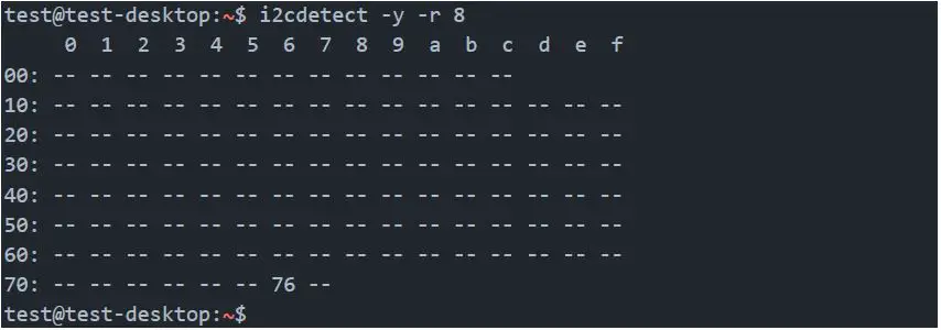
Dump i2c device registers
Syntax: i2cdump [options] <busNr> <deviceAddress>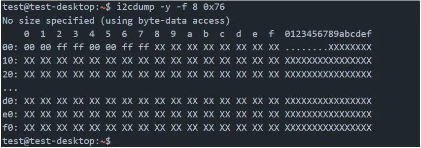
Set register value:
Syntax: i2cset [options] <busNr> <deviceAddress> <register> <address> <value>
- test@test-desktop:~$ sudo i2cset -y -f 8 0x76 0x06 0x00
- test@test-desktop:~$
Set register value:
Syntax: i2cset [options] <busNr> <deviceAddress> <register> <address> <value>
- test@test-desktop:~$ sudo i2cset -y -f 8 0x76 0x06 0x00
- test@test-desktop:~$
Read register value:
Syntax: i2cget [options] <busNr> <deviceAddress> <register> <address>
- test@test-desktop:~$ sudo i2cget -y -f 8 0x76 0x06 0x00
- test@test-desktop:~$
Test IMX219 camera stream
The parameter `sensor-id=` describes the camera target. This id can be found by using `ls /dev/`. If the camera is correctly plugged in then there should be a device called `/dev/videoX`, where X is the camera id.
- test@test-desktop:~$ gst-launch-1.0 nvarguscamerasrc sensor-id=0 ! ‘video/x-raw(memory:NVMM), width=(int)1280, height=(int)720, format=(string)NV12, framerate=(fraction)30/1’ ! nvvidconv! queue! xvimagesink


