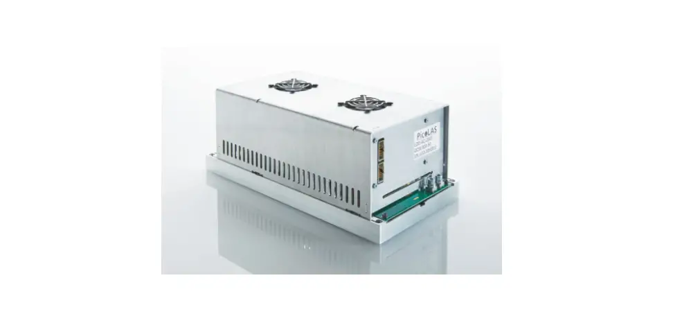
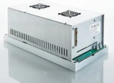
PicoLAS LDP-QCW 150 Cooled Laser Diode Driver
Product Information: LDP-QCW 150
The LDP-QCW 150 (LDP-QCW for short) is a high power linear regulated laser diode driver. It supports the following features:
- Supports up to 30 V compliance voltage
- Linear output driver for rectangular current pulses with ripple < 1 %
- Multiple trigger modes for external and internal triggering
- Interlock input for safety
Technical Specifications
| Output current | Compliance voltage | Min. pulse duration | Max. pulse duration | Max. repetition rate | Max. duty cycle | Max. rise time | Current overshoot | Pulse trigger input | Connectivity | Supply voltage | Max. power dissipation | Dimensions in mm | Weight | Operating temperature |
|---|---|---|---|---|---|---|---|---|---|---|---|---|---|---|
| *1: The compliance voltage strongly correlates to the pulse current and pulse duration. |
Product Usage Instructions
- Before powering on the unit, read the user manual thoroughly and make sure you understand everything. Pay attention to all safety warnings.
- If you have any doubt or suggestion, do not hesitate to contact PicoLAS GmbH.
- The LDP-QCW driver uses a DC-DC converter to load a capacitor bank to a defined voltage. It can provide a maximum voltage of 34 V
to load the storage capacitor bank Cb. - The driver implements a proportional integral (PI) regulator to control the current flow through the connected load. Make sure to be careful if changes are performed with the FFwd value.
- Available connectors and analogue interface specifications are described in the user manual.
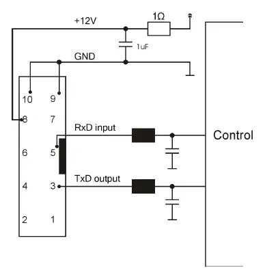
- Connect the PC to the driver using the standard RS-232 interface connection.
- Check all safety warnings before operating the unit.
Before powering on your unit, read this manual thoroughly and make sure you understood everything Please pay attention to all safety warnings.
If you have any doubt or suggestion, please do not hesitate to contact us.
Please pay attention to all safety warnings
How to use the Manual
Remark
The LDP-QCW 150 described in this manual is a primarily baseplate cooled laser diode driver. Improper cooling may cause an internal overtemperature shutdown.
Heat sink cooling with fans
Depending on the final application and operation regime a sufficient airflow created by the fans through the heat sink must be possible. Please refer to section “Cooling” for more details about the thermal power losses during operation. You may use a passive or an active air/water cooler. Before powering on your unit, read this manual thoroughly and make sure you understood everything.
Please pay attention to all safety warnings. If you have any doubt or suggestion, please do not hesitate to contact us!
Overview
The LDP-QCW 150 (LDP-QCW for short) is a high power linear regulated laser diode driver. It supports the following features:
- Supports up to 30 V compliance voltage
- Linear output driver for rectangular current pulses with ripple < 1 %
- Multiple trigger modes for external and internal triggering
- Interlock input for safety
Technical Specifications
| Output current | 1 .. 150 A |
| Compliance voltage | 0 .. 30 V *1 |
| Min. pulse duration | < 10 µs |
| Max. pulse duration | 1 ms |
| Max. repetition rate | 1 kHz |
| Max. duty cycle | 10 % |
| Max. rise time | TBD |
| Current overshoot | < 5 % (depending on regulator settings) |
| Pulse trigger input | Analog Interface: TTL |
| Connectivity | Analog interface, RS-232 |
| Supply voltage | 24 .. 48 V DC |
| Max. power dissipation | TBD |
| Dimensions in mm | 120 x 76 x 40 |
| Weight | 0.3 Kg |
| Operating temperature | 0 to +55 °C |
The compliance voltage strongly correlates to the pulse current and pulse duration.
Functional Description
The driver uses a DC-DC converter to load a capacitor bank to a defined voltage. It can provide a maximum voltage of 34 V to load the storage capacitor bank Cb. A P-I regulator using T1 and T2 are controlling the current flow through the laser diode. These regulators are triggered by an internal timing generator that is triggered by either an external trigger signal or via software through the RS-232 interface. Several security features protect the laser diode and the driver from damage. D1 protects the laser diode from reverse currents. The switch S1 is automatically opened when an internal failure or an interlock condition is detected.
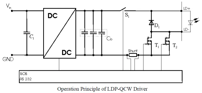
| Element | Function |
| C1 | Input buffer capacitor |
| Cb | Capacitor bank |
| S1 | Security switch |
| D1 | Laser diode protection diode |
| T1, T2 | Current regulation MosFET |
| Shunt | LD current monitor |
Current Regulator
The LDP-QCW implements a proportional integral (PI) regulator to control the current flow through the connected load. The following diagram shows a simplified layout:
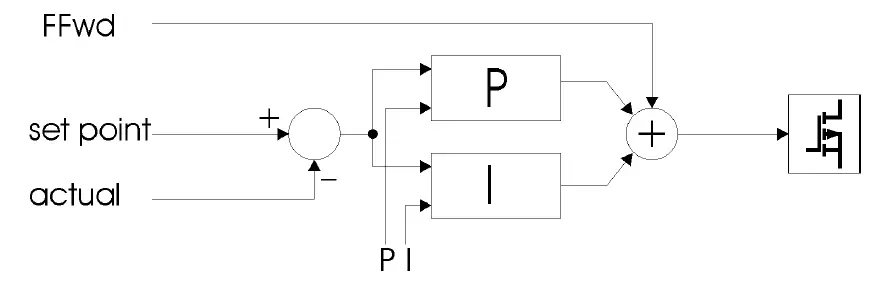
Depending on the chosen operating mode the user has the possibility to modify all relevant parameters to a specific need. This is done through the digital interface (RS-232). See below for more information. Picoulas implemented an active nonlinearity compensation of the output stage. This speeds up the device, prevents excessive current overshoots and yields a better accuracy with high impedance loads. The influence of this part of the regulator can be user defined and is called Fad. However, the interconnection between the voltage and the current flow on the output is calibrated during fabrication. This is used in operating mode 1. So, it is not necessary to change this value if only these operating modes are used. If needed, it can be adjusted between the values 0 to 7.5 by the customer. Be careful if changes are performed with the FFwd value. The effect is high and may cause damage to the connected load if not adjusted properly. Wrong settings are not covered by warranty.
Description of available Connectors
Analogue Interface Specifications
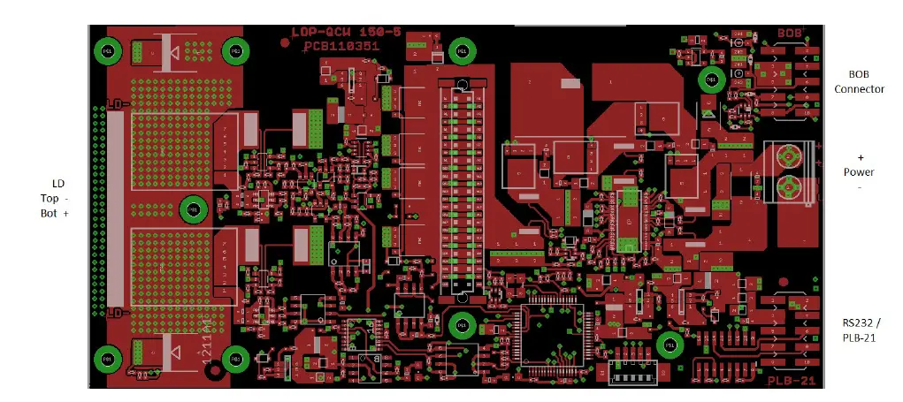
The following figure shows the input and output signals of the external analogue BOB connector. The LDP-C BOB (Breakout board) is recommended for easy testing of the driver. It will be replaced in the application by your machine interface.
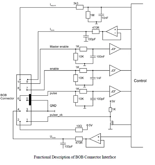
Pin Description (numerical assorted)
Pin 1: Pulser OK
The state of this signal indicates weather the driver is ready (5 V) or it has an error pending (0 V).
Pin 2: 5 V
This pin provides 5 Volts for external usage. Please note that the load should not exceed 10 mA, otherwise the voltage will drop.
Pin 3: GND
This pin is connected to ground.
Pin 4: Udiode
This signal provides near real time measurement of the laser diodes compliance voltage. The scaling is 10 Volts per Volt measured into 1 MOhm.
Pin 5: GND
This pin is connected to ground.
Pin 6: Pulse
This signal is used in the external end external controlled trigger mode. Connect your external trigger source to this pin. The signal amplitude should be within 3 to 6 Volts.
Pin 7: Enable
This signal is used to enable / disable the current output of the driver during operation.
It must be pulled low to reset an error condition or to re-enable the driver after Master Enable was pulled low.
Pin 8: Master Enable
This signal is used as an interlock safety feature that disables the complete driver if set to 0 V during operation. In order to re-enable the driver after this emergency shutdown the enable signal must first set to 0 V. If this feature is not required this pin can be connected to pin 2 (5 V).
Pin 9: Idiode
This signal provides near real time measurement of the laser diodes current flow. The scaling is 200 Amperes per Volt measured into 1MOhm.
Pin 10: Isetpoint
This pin is not used in this driver.
The interface is a standard RS-232 interface connection. It can be used to connect the PC to the driver.
How to get started
| Step | What to do | Check |
| 1 | Unpack your device and place it in front of you as shown on the next page. | |
| 2 | Connect a load (for example your laser diode) to the output. | |
| 3 | Connect the RS-232 cable / PLB-21 | See section “Controlling the LDP- QCW via RS-232” for more information. |
| 4 | Connect the input power supply. Make sure that polarity is correct. The supply voltage is 24 V .. 48 V. | Make sure that your power supply does not have any voltage overshoots when switching on or off. Do not exceed the maximum operating voltage of 52 V. |
| 5 | Switch the power supply on. | |
| 6 | Set all required parameters using the RS-232 interface. Make sure that the capacitor voltage is set to a safe value. | See section “Controlling the LDP- QCW via RS-232” for more information. |
| 7 | Apply +5 V to the interlock pin of the BOB connector. This will enable internal power conditioner. | See section “Interface Specifications” for more information. |
| 8 | Apply +5 V to the Enable pin of the BOB connector. This will enable the output. | See section “Interface Specifications” for more information. |
| 9 | Monitor the current pulses using an oscilloscope connected to the current monitor output. | See section “Interface Specifications” for more information. |
Cooling
The maximum thermal dissipation of the LDP-QCW depends on the configured pulse length, repetition rate and capacitor bank voltage. The driver is cooled by a heat sink and two fans for continuous high-power operation. The maximal thermal dissipation can be estimated by:
![]()
where
- PL Thermal dissipation loss in W
- Vcap Capacitor voltage in V
- VLD Compliance voltage of the LD in V
- d Duty cycle in percent
- ILD Laser diode current
- PS Static operation losses ~ 7 W
This is only an approximation and achieved values can differ. Carefully monitor the temperature of the driver and the heat sink for new operational conditions.
Test Load
A common method to test the driver is to connect a regular silicon rectifier diode to the driver output. Please pay attention to the junction capacitance of the diode. Only fast recovery diodes (or similar) have a low parasitic capacitance comparable to laser diodes. To achieve reasonable test results, the parasitic elements of the test diode and the connection must be very similar to a laser diode approach. Regular silicon rectifier diodes have a junction
capacitance of several microfarads and are not a suitable test load! The use of these diodes will yield in incorrect current measurement at the pulse edges! It is also possible to test the driver using a shortcut. This will not damage it, but result in an incorrect measurement for the rise and fall time of the current pulse.
Digital Interface Specifications
The interface provides the following connections:
- RS-232 interface
- Interlock input
- Enable input
- Trigger input
The RS-232 interface gives access to all internal settings and registers. It uses a communication speed of 115200 baud with 8 data bits, 1 stop bit and even parity. In order to test the interface connection, the PING or infit command may be used, depending on which protocol should be used. It does not change any settings of the driver. The interlock input signal controls the internal power conditioner as well as the pulse output stage. It must be enabled before the enable signal. Otherwise, the driver enters an error condition and will not produce any output current. If the interlock drops during normal operation, the power conditioner as well as the current output is disabled and the capacitor bank is discharged. The enable signal must be disabled before the interlock can be re-enabled.
The storage discharge slowly. Be careful when powering off the driver as they may still hold a high voltage. Touching them might result to an electrical shock.
The enable input controls the current regulator and the internal trigger generator. When it is enabled, the driver will generate output pulses according to the configured settings. The trigger input is used in the external trigger mode. When configured, it will control the output current generation. The trigger output signal provides a signal with the same pulse width and repetition rate as the current output.
Power Supply
To obtain a good pulsing performance with the driver, it requires an appropriate power supply unit (PSU). The PSU has to supply not only the power that is delivered to the laser diode but also the power to compensate for the losses in the driver itself. The device is equipped with a buck-boost DC-DC converter which allows it to generate a capacitor voltage that is higher than the input voltage.
PC Interface
As described in the interface specifications the PC interface uses the RS-232 standard with the connection settings of 115200 baud, 8 data bits, 1 stop bit and even parity. In order to initialize the Picoulas protocol, the PING command is used. To initialize the text protocol, use the infit command. The acknowledgement of this command indicates a successful communication.
PLB-21
To use the PLB-21 to control the driver, simply connect it using the cable supplied with the PLB-21. No further actions are required as the driver supplies all required signals (communication and power) to the PLB-21. The menu structure is described in chapter XXXX.
Pulse current
The LDP-QCW is capable of generating a single rectangular shaped current pulse. The pulse current, pulse width and repetition rate can be configured via RS-232 / PLB-21 or via the BOB interface connector.
In the current hardware revision, the pulse current can only be set via digital interface.
Regulator Operation Modes
T the driver’s current regulator offers two different operation modes, which applies to both pulse shape modes.
Mode 0: manual
In this operation mode all parameters can be modified.
This mode is recommended only for experienced users as any wrong setting may lead to a significant current overshoot at the output.
Mode 1: semi-auto
In this operation mode the feed forward (Fad) value is automatically chosen in dependence of the current setpoint. This is recommended for normal operation as it guarantees minimal current overshoot at the output.
Capacitor Voltage
The capacitor bank is charged by an internal DC-DC converter. It transforms the supply voltage into a configurable capacitor voltage. The power conversion is controlled by the interlock input. Setting the interlock to “1” while the enable signal is “0” will start the capacitor loading procedure. If the enable signal is given before the interlock, the driver will enter an error condition and no power is transferred into the capacitors. The capacitor voltage is controlled by the SETVCAP / scup command. It must be set by the operator to a value that depends on the chosen pulse width, repetition rate and compliance voltage. If his value is too low the current will drop during the pulse or not even reach the setpoint, if it is too high the output stage will heat up fast and lead to an overtemperature shutdown. The following equation can be used to calculate the capacitor voltage vape in dependence of the output current, compliance voltage and pulse width:
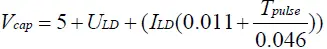
where
- ULD Compliance voltage in V
- ILD Current setpoint in A
- Tpulse Pulse width in s
This equation does not use the repetition rate. Hence, this value must be increased if a current drop is measured during operation.
If the capacitor voltage is way too high, the output stage can get damaged. It is safe to start with a lower than required voltage and raise it slowly during operation until the pulse shape is rectangular. The storage capacitors provide a high amount of energy. Creating a short cut over the output clamps is not recommended and might result in an electrical spark and / or fire. The capacitors are charged up to 34 V. Touching the clamps may result in an electrical shock and serious injury.
Trigger Modes
The LDP-QCW supports four different trigger modes as explained below. In order to change the trigger mode, the driver must be disabled (enable = 0) and the TRG_MODE and
TRG_EDGE bits in the LSTAT register must be set accordingly.
Internal (trgmode = 0)
The pulse generation is performed by an internal pulse generator. The pulse width and repetition rate are user configurable via the serial interface. In addition, the number of pulses that will be generated when the driver is enabled can be set from a single pulse to a continuous pulse generation while the driver is enabled. The following diagram shows an example of generated pulses. The lower graph shows the internal pulse generator, the upper two graphs the trigger pulses generated out of it.
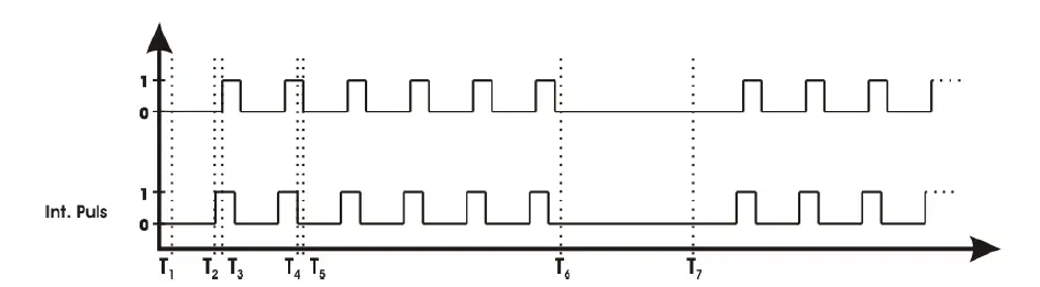
| Symbol | Meaning |
| T1 | Enabling of the output. |
| T1-T2 | Delay between output enable and the first generated pulse depends on the configured repetition rate. It nearly equals the pulse pause time. |
| T2-T3 | Pulse rise time. It depends on the load inductance. |
| T4-T5 | Pulse fall time. It depends on the load inductance. |
| T6 | Disabling of the output. |
| T7 | Re-enabling of the output. |
External (trgmode = 1)
The pulse generation is performed by an external pulse generator connected to the pulse input on the BOB connector. The pulse width and repetition rate is defined by the trigger signal. The pulses can be inverted by setting the TRG_EDGE bit in the LSTAT register to “0” or “1”.
The following diagram shows an example of generated pulses. The lower graph shows the external pulse input, the upper two graphs the trigger pulses generated out of it.
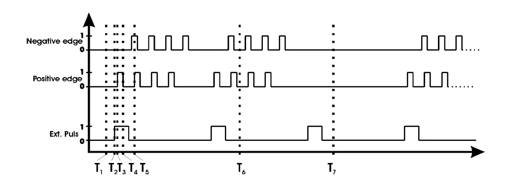
| Symbol | Meaning |
| T1 | Enabling of the output. |
| T2-T3 | Pulse rise time. It depends on the load inductance. |
| T4-T5 | Pulse fall time. It depends on the load inductance. |
| T6 | Disabling of the output. |
| T7 | Re-enabling of the output. |
External controlled (trg mode = 2)
This trigger mode uses the external trigger input to control the internal pulse generator. It is used to generate a number of pulses per rising or falling edge of the external trigger input. The pulse width and repetition rate are defined by the internal pulse generator and can be set using the serial interface. Hence, only the edge of the trigger signal is utilized. Setting the TRG_EDGE bit in the LSTAT register to “1” uses the rising edge, setting it to “0” uses the falling edge.
The number of pulses and the repetition rate can be set via software.
The following diagram shows an example of generated pulses. The lower graph shows the external pulse input, the upper two graphs the trigger pulses generated out of it.
| Symbol | Meaning |
| T1 | Enabling of the output. |
| T2-T3 | Pulse rise time. It depends on the load inductance. |
| T4-T5 | Pulse fall time. It depends on the load inductance. |
| T6 | Disabling of the output. |
| T7 | Re-enabling of the output. |
Software (trimodal = 3)
This trigger mode works exactly like the external controlled mode. The only difference is that the trigger is given using a software command.
Output Enable
The output stage of the driver is controlled by the interlock and the enable signal. Setting the enable to “1” while the interlock is given, the driver will start to produce output current pulses according to the selected trigger mode. The driver will produce output current as long as the trigger condition is matched and the enable and interlock signals are given. Setting the enable signal to “0” will disable the output.
Setting the interlock signal to “0” while the enable signal is given will disable the output stage, discharge the capacitor bank and put the driver into an error condition. This is reset by setting the enable signal to “0”.
Alternatively, the enable signal can be controlled via software. Set the ENABLE_EXT bit in the LSTAT register to “0” to switch to software control. If the text protocol is used, the commands are enable nit, enable ext., enable and disable.
Output disable
The driver’s output is disabled by setting the enable signal to “0”. This will disable the internal pulse generator and therefore the current output.
If the internal enable control is used, use the disable command.
Exchange Dummy Load for Laser Diode
Before removing the dummy load, it is recommended to set the interlock signal to “0” as well. This will discharge the capacitor bank and put the driver into a safe condition. After setting interlock to “0”, the capacitors require a certain amount of time to discharge. Before working on the capacitor or output clamps make sure that there is no residual voltage.
Timing Diagram
The following diagram shows the effect of the MEN (Master Enable), ENABLE and trigger input signals to the external current flow:
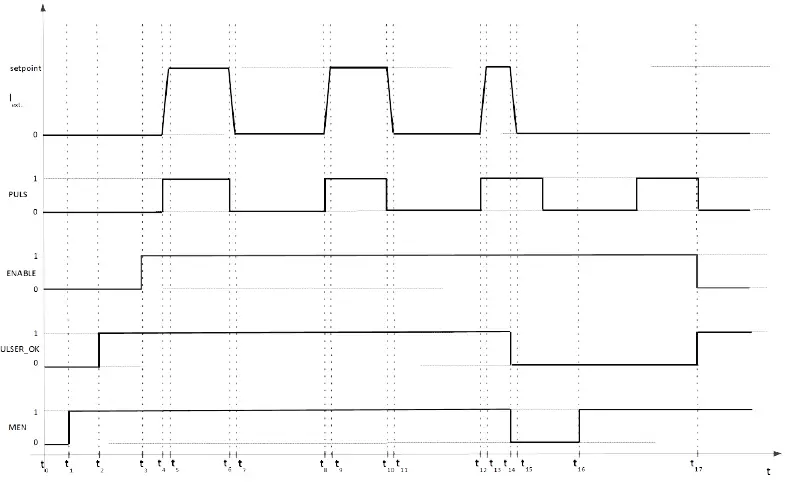
| Symbol | Meaning | Min. | Max. | Avg. | Description |
| t1 | MEN given | ||||
| t0 – t2 | Power on self test | 2.5 s | 14 s | 4 s | |
| t3 | ENABLE given | ||||
| t4 – t5 t8 – t9 t12 – t13 | Rise time | 1 µs | Depends on the inductance of the connected load. | ||
| t6 – t7 t10 – t11 t14 – t15 | Fall time | Depends on the inductance of the connected load. | |||
| t14 | MEN released | Output current drops to zero, driver in error state. | |||
| t17 | MEN state reset | Driver is operational again. |
Dos and Don’ts
- Never ground any output connector.
- Never use any grounded probes at the output.
- Do not connect your oscilloscope to the output!
- This will immediately destroy the driver and the probe!
- For measuring current and voltage you connect the scope to pin 9 or pin 4 of the BOB connector respectively.
- Never create a short over the capacitor clamps while the capacitors contain energy!
- Keep connecting cables between power supply and driver as well as the connection between driver and laser diode as short as possible.
- Mount the driver on an appropriate heat sink!
Please be aware that there might be hot surfaces, be careful not to touch them.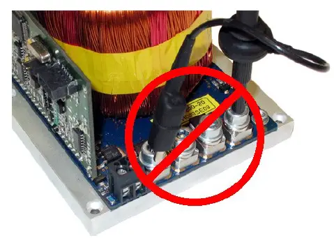 Do never connect the oscilloscope to the output connectors!!!! (Please note: above picture shows another but similar PicoLAS driver).
Overtemperature Shutdown
To protect the laser diode and the driver itself, the LDP-QCW automatically disables itself if its temperature rises above the maximum allowed operating temperature. This condition is latched and the LDP-QCW will not start working until temperature drops five degrees and the ENABLE signal is toggled.
If an Error Occurs
If an error occurs during operation the pulse output is switched off. All error conditions are latched and cleared by disabling the driver (either using the switch or the software control).
Mechanical Dimensions
The following dimensions are in millimeters (mm). Please note that the picture is horizontally compressed.
Controlling the LDP-QCW via RS-232
Introduction
The RS-232 interface allows communications over a serial text interface as well as using the PicoLAS protocol. While the text interface is designed for communication with a terminal program, the PicoLAS protocol is designed as a system interact protocol.
The switching between the two protocols occurs automatically as soon as the LDP-QCW receives a certain sequence. The corresponding commands are:
- PING for the Picolas protocol
- “infit” followed by <Enter> for the text interface
The connection settings are:
- Baud rate : 115200
- Data bits : 8
- Stop bits : 1
- Parity : even
The Serial Text Interface
The following section describes the structure and commands of the text interface.
Structure
Every command that is sent to the LDP-QCW must be completed with a CR (Enter). It consists of a command word followed by one ore more parameters. If the command was successfully executed a “00” is sent, otherwise a “01”. If there is an error pending, the response will be “10”, otherwise “11”. If the command requires an answer parameter, this parameter is sent before the confirmation is given.
Example:
The user would like to read out the actual setpoint current:
User input: gaur <Enter>
Output of the LDP-CW: 150.0<CR><LF> 00<CR><LF>
Example 2:
The user would like to set a new setpoint current:
User input: scur 100.5<Enter>
Output of the LDP-CW: 100.5<CR><LF> 00<CR><LF>
Input is done in ASCII code and is case sensitive. Every terminal can be used that supports this standard.
Commands for the serial text interface
The following table contains a command reference for the LDP-QCW
| Command | Parameter | Description |
| ghwver | – | returns the hardware version number |
| gswver | – | returns the software version number |
| gserial | – | returns the serial number |
| gname | – | returns the device name |
| ps | – | prints out all settings |
| loaddef | – | load default values |
| savedef | – | save all settings as default values |
| enautodef | – | enables the automatic loading of default settings on power on |
| disautodef | – | disables the automatic loading of default settings on power on |
| gerrtxt | – | returns the error register in text form |
| gerr | – | returns the error register as a 32-bit number |
| clrerr | – | clears the error register |
| glstat | – | returns the laser status register |
| slstat | 32-bit number | sets the laser status register to the given value |
| gtrgedge | – | returns “0” for negative edge or “1” for positive edge |
| strgedge | 0 or 1 | sets the trigger edge for external trigger “0” = negative, “1” = positive |
| gmode | – | returns the current regulator mode Mode 0: manual Mode 1: semi-automatic
See section “Current Regulator” for more information |
| smode | 0 … 1 | sets the current regulator mode to the given value Mode 0: manual Mode 1: semi-automatic
See section “Current Regulator” for more information |
| Command | Parameter | Description |
| gcur | – | returns the actual setpoint current in [A]. |
| gcurmin | – | returns the minimum setpoint current. |
| gcurmax | – | returns the maximum setpoint current. |
| scur | <current> | sets the internal setpoint current to the given value. This value must be within the minimum/maximum borders (see above). One position after decimal point is used (e.g. 80.5). The return value is the new setpoint. |
| gwidth | – | returns the actual pulse width in [us]. |
| gwidthmin | – | returns the minimum possible pulse width in [us]. |
| gwidthmax | – | returns the maximum possible pulse width in [us]. |
| swidth | <width> | sets the pulse width for the pulse. Please note that any change in this register affects the maximum possible repetition rate. The return value is the new pulse width. |
| grepratemin | – | returns the actual repetition rate in [Hz] |
| grepratemin | returns the minimal possible repetition rate in [Hz] | |
| grepratemax | returns the maximal possible repetition rate in [Hz] | |
| serrate | reprate in [Hz] | sets the pulse repetition rate to the given value. The return value is the new repetition rate. |
| gvcap | – | returns the actual pre charge voltage of the internal capacitor bank in [V] |
| gvcapmin | – | returns the minimum pre charge voltage of the internal capacitor bank in [V] |
| gvcapmin | – | returns the maximum pre charge voltage of the internal capacitor bank in [V] |
| scup | voltage in [V] | sets the pre charge voltage of the internal capacitor bank to the given value in [V] |
| sffwd | – | returns the actual voltage of the feed forward part of the current regulator in [V]. See section “Current Regulator” for more information. |
| sffwd | <voltage> | sets the feed forward voltage to the given value. Two positions after decimal point are used (e.g. 3.45). It must be within the borders of gffwdmin / gffwdmin. |
| gffwdmin | – | returns the minimum possible value of the feed forward voltage in [V] |
| gffwdmin | – | returns the maximum possible value of the feed forward voltage in [V] |
The PicoLAS protocol
The following section describes the structure and commands of the Picolas protocol.
Picolas Protocol Structure
The protocol uses a frame-based structure. Each frame consists of 7 bytes which must be sent consecutively. Otherwise, the protocol will time out and the transmission must start again. For each valid frame received, an answer is sent to the host after it has processed the command. If a second frame is sent before an answer has been received, it may by declared invalid and become discarded. Each protocol frame consists of 7 bytes. The first two are interpreted as a 16-bit command word followed by a 32-bit data word and an 8-bit checksum. Each of the words are little endian encoded. This leads to the following structure:
Protocol frame
| Protocol frame | |||||||
| Byte | 0 | 1 | 2 | 3 | 4 | 5 | 6 |
| Meaning | Command | Command | Data | Data | Data | Data | CRC |
| Bits | 0 .. 7 | 8 .. 15 | 0 .. 7 | 8 .. 15 | 16 .. 23 | 24 .. 31 | 0 .. 7 |
The CRC byte is calculated by an XOR of the six other bytes of the frame. Any frame received with an invalid checksum is discarded without further notice.
Commands
The Driver has a wide range of control commands. In certain operation conditions one or more commands may not be available. In this case, the driver will answer with UNAVL (0xFF14) and the relating command as parameter.
- If an unknown command is received, the driver will answer with UNCOM (0xFF13).
- If it receives a valid command with an invalid data value, it will answer with ILGLPARAM (0xFF12).
- The following commands are available:
General
These commands have various general functions.
| Command Name | Command frame | Answer frame | ||
| Command | Data | Command | Data | |
| PING | 0xFE01 | 0 | 0xFF01 | 0 |
| IDENT | 0xFE02 | 0 | 0xFF02 | Device ID |
| GETHARDVER | 0xFE06 | 0 | 0xFF06 | Hardware version |
| GETSOFTVERST | 0xFE07 | 0 | 0xFF07 | Software version control board |
| GETSERIAL | 0xFE09 | 0 | 0xFF09 | Device serial number |
| GETIDSTRING | 0xFE08 | 0 | 0xFF08 | Device description string |
Temperature
These commands give access to the driver’s temperature monitor functions.
| Command Name | Command frame | Answer frame | ||
| Command | Data | Command | Data | |
| GETTEMP | 0x0101 | 0 | 0x8100 | Int32 in 0.1 °C |
| GETTEMPOFF | 0x0102 | 0 | 0x8100 | Int32 in 0.1 °C |
| GETTEMPMAX | 0x0103 | 0 | 0x8100 | Int32 in 0.1 °C |
| GETTEMPHYS | 0x0104 | 0 | 0x8100 | Int32 in 0.1 °C |
LSTAT Register
These commands give access to the driver’s status and control register. Any write access using the SETLSTAT command is executed immediately. Some of the bits are read only or only writeable under certain conditions. Please refer to the LSTAT register description later in this document for more information.
| Command Name | Command frame | Answer frame | ||
| Command | Data | Command | Data | |
| GETLSTAT | 0x0200 | 0 | 0x8200 | Uint32 register |
| SETLSTAT | 0x0201 | Uint32 register | 0x8200 | Uint32 register |
ERROR Register
These commands give access to the driver’s error registers. These are read only and will be cleared if the error condition is removed and the enable signal is toggled or the CLEARERROR command is received. Please refer to the ERROR register description later in this document for more information.
| Command Name | Command frame | Answer frame | ||
| Command | Data | Command | Data | |
| GETERROR_1 | 0x0300 | 0 | 0x8300 | Uint32 register |
| CLEARERROR | 0x0301 | 0 | 0x8300 | 0 |
Pulse generation
These commands give access to the driver’s internal pulse generator. Depending on the used trigger mode or the channels are locked not all commands are available. In that case, the answer frame will contain the command 0xFF14 (UNAVL).
| Command Name | Command frame | Answer frame | ||
| Command | Data | Command | Data | |
| GETWIDTH | 0x0400 | 0 | 0x8400 | Uint32 in us |
| GETWIDTHMIN | 0x0401 | 0 | 0x8400 | Uint32 in us |
| GETWIDTHMAX | 0x0402 | 0 | 0x8400 | Uint32 in us |
| SETWIDTH | 0x0403 | Uint32 in us | 0x8400 | Uint32 in us |
| GETREPRATE | 0x0404 | 0 | 0x8400 | Uint32 in 0.1 Hz |
| GETREPRATEMIN | 0x0405 | 0 | 0x8400 | Uint32 in 0.1 Hz |
| GETREPRATEMAX | 0x0406 | 0 | 0x8400 | Uint32 in 0.1 Hz |
| SETREPRATE | 0x0407 | Uint32 in 0.01 Hz | 0x8400 | Uint32 in 0.1 Hz |
| GETCOUNT | 0x0408 | 0 | 0x8400 | Uint32 |
| GETCOUNTMIN | 0x0409 | 0 | 0x8400 | Uint32 |
| GETCOUNTMAX | 0x040A | 0 | 0x8400 | Uint32 |
| SETCOUNT | 0x040B | Uint32 | 0x8400 | Uint32 |
| EXECPULS | 0x040C | 0 | 0x8400 | 0 |
Capacitor Voltage
These commands give access to the capacitor bank pre charger.
| Command Name | Command frame | Answer frame | ||
| Command | Data | Command | Data | |
| GETVCAP | 0x0500 | 0 | 0x8500 | Uint32 in 0.1 V |
| GETVCAPMIN | 0x0501 | 0 | 0x8500 | Uint32 in 0.1 V |
| GETVCAPMAX | 0x0502 | 0 | 0x8500 | Uint32 in 0.1 V |
| SETVCAP | 0x0503 | Uint32 in 0.1 V | 0x8500 | Uint32 in 0.1 V |
Current control
These commands give access to the current regulator.
| Command Name | Command frame | Answer frame | ||
| Command | Data | Command | Data | |
| GETCUR | 0x0600 | 0 | 0x8600 | Uint32 in A |
| GETCURMIN | 0x0601 | 0 | 0x8600 | Uint32 in A |
| GETCURMAX | 0x0602 | 0 | 0x8600 | Uint32 in A |
| SETCUR | 0x0603 | Uint32 in A | 0x8600 | Uint32 in A |
Analogue digital converter
These commands give access to the analogue to digital converter and its internal and pulse measurements.
| Command Name | Command frame | Answer frame | ||
| Command | Data | Command | Data | |
| GETADCUDIODE | 0x00C0 | 0 | 0x01C0 | Uint32 in V |
| GETADCIDIODE | 0x00C1 | 0 | 0x01C0 | Uint32 in A |
| GETADCVCAP | 0x00C2 | 0 | 0x01C0 | Uint32 in 0.1 V |
| GETADCUIN | 0x00C5 | 0 | 0x01C0 | Uint32 in 0.1 V |
Default values
These commands give access to the driver’s default value set. Each operating parameter can be saved to this default set and recalled later.
| Command Name | Command frame | Answer frame | ||
| Command | Data | Command | Data | |
| LOADDEFAULTS | 0x0800 | 0 | 0x0800 | 0 |
| SAVEDEFAULTS | 0x0801 | 0 | 0x0800 | 0 |
Feed Forward (FFwd)
These commands give access to the current regulators feed forward part. These commands are only used, if the current regulator is set to mode 0 and should be used with caution. If the regulator is in any other mode, the answer frame will contain the command 0xFF14 indicating that the command is unavailable.
| Command Name | Command frame | Answer frame | ||
| Command | Data | Command | Data | |
| GETFFWD | 0x1000 | 0 | 0x9000 | Uint32 in 0.01 V |
| SETFFWD | 0x1001 | Uint32 in 0.01 V | 0x9000 | Uint32 in 0.01 V |
| GETFFWDMIN | 0x1002 | 0 | 0x9000 | Uint32 in 0.01 V |
| GETFFWDMAX | 0x1003 | 0 | 0x9000 | Uint32 in 0.01 V |
Description of the LSTAT Register
The following list contains a description of the individual LSTAT bits. These can be read with the GETLSTAT and written with SETLSTAT command.
| Bit | Name | Read/Write | Meaning |
| 0 | ENABLE_OK | ro / r/w | Indicates the state of the ENABLE signal. When ENABLE_EXT is “0”, this bit is used to control the driver’s output |
| 1 | PULSER_OK | ro | When the bit is read “0” an error has occurred |
| 2 | DEF_PWRON | r/w | When “1” the device loads its default values on power on. |
| 3 | TRG_EDGE | r/w | When “1” the positive edge is used. |
| 4 | reserved | ro | |
| 5 | ENABLE_LOCK | or | Indicates, that the Enable pin must be set to “0” in order to continue normal operation. |
| 6-7 | TRG_MODE | r/w | Trigger mode: 0: internal 1: external 2: external controlled 3: software controlled |
| 8 | MASTER_ENABLE | or | Indicates the state of the interlock pin. |
| 9 | ENABLED | or | Indicates weather the driver’s output is enabled of not |
| 10 | ENABLE_EXT | r/w | When “1” the external enable input is used to control the driver |
| 11 | CUR_EXT | r/w | When “1” the external analogue current input pin is used to control the current setpoint. Please note: Not used in the current hardware revision. |
| 12-13 | REGLER_MODE | r/w | Current regulator mode: 0: manual 1: semi-auto 2: manual + VCAP antitracking 3: semi-auto + VCAP antitracking |
| Bit | Name | Read/Write | Meaning |
| 14 | EXEC_SW_PULSE | r/w | When “1”, the driver will execute a pulse (in trigger mode 3). |
| 15 | EXECUTING_PULSES | or | Indicates that the driver is currently executing a software trigger. |
| 16 | ABORT_EXEC_PULSES | r/w | When “1”, the driver will abort the current software trigger. |
| 17 | DIS_INTEGRAL | or | Controls the integral part of the current regulator: 0: Enabled (default) 1: Disabled |
| 18-31 | reserved | or | reserved |
Description of the ERROR Registers
The device has two 32-bit wide error registers. The following lists contain a description of the individual bits of each register. Unless otherwise noted, a “1” indicates an error or warning condition.
| Bit | Name | Read/ Write | Meaning |
| 0 | CRC_DEVDRV_FAIL | ro | A CRC error was detected in the internal PLB-21 driver. Please contact your distributor. |
| 1 | CRC_DEFAULT_FAIL | or | A CRC error was detected in the default values. A re-save of the values should correct this. |
| 2 | CRC_CONFIG_FAIL | or | A CRC error was detected in the internal configuration values. Please contact your distributor. |
| 3 | reserved | or | reserved |
| 4 | CRC_FFWDCAL_FAIL | or | Indicates that the feed forward calibration of channel 1 is faulty. |
| 5 | CRC_ISOLLCAL_FAIL | or | Indicates that the current setpoint calibration of channel 0 is faulty. |
| 6 | TEMP_OVERSTEPPED | or | The internal temperature was beyond safe operating limits. |
| 7 | TEMP_WARNING | or | The internal temperature is 5 °C before shutdown. |
| 8 | TEMP_HYSTERESE | or | Device is cooling down. Temperature needs to drop below (maximum – 10 °C) |
| 9 | VCC_FAIL | or | Internal supply voltage error. |
| 10 | FAIL_DEFAULTS | or | The loading of the default failed. Normally this is because of a pending CRC error. |
| 11 | I2C_EEPROM_FAIL | or | Internal EEProm error. Please contact your distributor. |
| 12 | I2C_DAC_FAIL | or | Internal DAC error. |
| 13 | I2C_RD_FAIL | or | Indicates an I²C read error. |
| 14 | I2C_WR_FAIL | or | Indicates an I²C write error. |
| 15 | ENABLE_POWERON | or | Indicates that the ENABLE signal was given during start-up. |
| 16 | TEMP_SENSOR_FAIL | or | A “1” indicates an error. |
| 17-31 | reserved | or | Reserved |
Impresseum
Picolas GmbH
Burg Strasse 2 52146 Würselen Germany
- Phone: +49 (0) 2405-64594-60
- Fax: +49 (0) 2405-64594-61
- E-Mail: [email protected]
- Web: www.picolas.de
- CEO: Dr.-Ing. Markus Bartram
- Registration Court: Amtsgericht Aachen
- Registration Number: HRB 13040
- Tax ID (Ust. IdNr.): DE 243221335
- WEEE-Reg.-Nr.: DE 28806084
No liability will be accepted for errors and omissions. Technical modifications reserved.


