
 SanDisk industrial micro SD Card
NOTICE/DISCLAIMER
SanDisk provides this information, and any related samples, products, and documentation (collectively the “Materials”) solely for the selection and use of SanDisk products. To the maximum extent permitted by applicable law: (1) Materials are made available “AS IS” and with all faults, SanDisk hereby DISCLAIMS ALL WARRANTIES AND CONDITIONS, EXPRESS, IMPLIED, STATUTORY, OR OTHERWISE, INCLUDING BUT NOT LIMITED TO WARRANTIES OF MERCHANTABILITY, NON-INFRINGEMENT, OR FITNESS FOR ANY PARTICULAR PURPOSE; and (2) SanDisk shall not be liable (whether in contract or tort, including negligence, or under any other theory of liability) for any loss or damage of any kind or nature related to, arising under, or in connection with, the Materials (including your use of the Materials), including for any direct, indirect, special, incidental, or consequential loss or damage (including loss of data, profits, goodwill, or any type of loss or damage suffered as a result of any action brought by a third party) even if such damage or loss was reasonably foreseeable or SanDisk had been advised of the possibility of the same. You are responsible for obtaining any rights required in connection with your use of the Materials. The Materials are subject to change without further notice. SanDisk assumes no obligation to correct errors or to notify you of updates to the Materials or to product specifications. You may not reverse engineer, reproduce, modify, distribute, or publicly display the Materials without prior written consent of SanDisk. SanDisk products are not designed or intended to be fail-safe or for use in any application requiring fail-safe performance. You assume sole risk and liability for use of SanDisk products in critical applications.
© 2016 SanDisk Corporation. All rights reserved. Specifications are subject to change. SanDisk is a trademark of SanDisk Corporation, registered in the United States and other countries. SD, SDHC, SDXC are all trademarks of SD-3C, LLC. Other brand names mentioned herein are for identification purposes only and may be the trademarks of their respective holder(s).
02-05-WW-02-00005 December 2015. Printed in the United States of America.
INTRODUCTION
General Description
The SanDisk Industrial microSD Card is a flash-based removable non-volatile memory device specifically designed to meet the security, endurance, capacity, performance and environmental requirements inherent in next-generation industrial and consumer electronic devices.
The SanDisk Industrial microSD Card is based on an 8-pin interface designed to operate in a maximum operating frequency of 104 MHz. The interface for SD Card products allows for easy integration into any design, regardless of which type of microprocessor is used. In addition to the interface, SD Card products offer an alternate communication protocol based on the SPI standard.
SanDisk Industrial microSD cards are designed especially for use in mass storage applications. In addition to the mass storage-specific flash memory. SanDisk Industrial microSD cards include an onboard intelligent controller which manages interface protocols; security algorithms for content protection; data storage and retrieval, as well as Error Correction Code (ECC) algorithms; defect handling; power management; wear leveling and clock control.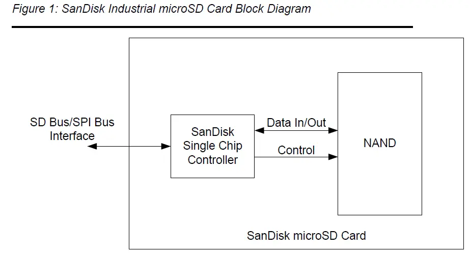
Features
General features of cards in the SanDisk Industrial microSD Card include:
- SD-protocol compatible
- Supports SPI Mode
- Targeted for Industrial applications for secured (content protected) and unsecured data storage
- Voltage range of 2.7 to 3.6V
- Variable clock rate 0-25 MHz (standard), 0-50 MHz (high performance). 0-104MHz (Ultra High Speed)
- Up to 50 MB/sec data transfer rate (using four parallel data lines)
- Memory field error correction
- Password protection
- Write protection using a mechanical switch
- Built-in write protection features (permanent and temporary)
- Supports card detection (insertion and removal)
- Application-specific commands
Additional features supported in 32GB and 64GB SanDisk Industrial microSD Cards:
- Device health status
- Programmable string
- Host lock
- Secured field firmware update (SFFU)
- Read refresh
- Enhanced power immunity
Scope
This document describes key features and specifications of the SanDisk microSD Card as well as the information required to interface this product to a host system. Chapter 2 describes the physical and mechanical properties of cards in the SanDisk SD Card, Chapter 3 contains the pins and register overview, and Chapter 4 gives a general overview of the SD protocol. Information about SPI Protocol can be referenced in Section 7 of the SDA Physical Layer Specification, Version 3.01.
SD Card Standard
SanDisk microSD cards are fully compatible with the SDA Physical Layer Specification, Version 3.01. This specification is available from the SD Card Association (SDA).
SD Card Association 2400 Camino Ramon, Suite 375 San Ramon, CA 94583
USA
Telephone: +1 (925) 275-6615 Fax: +1 (925) 886-4870
E-mail: [email protected] Web site: www.sdcard.org
Functional Description
The family of SanDisk Industrial microSD cards contains a high-level, intelligent subsystem as shown in Figure 1-1. This intelligent (microprocessor) subsystem provides many capabilities not found in other types of memory cards. These capabilities include:
- Host independence from details of erasing and programming flash memory
- A sophisticated system for managing defects (analogous to systems found in magnetic disk drives)
- A sophisticated system for error recovery including a powerful ECC
- Power management for low-power operation
- Auto read refresh capability to maximize read endurance of the memory
- Enhanced power immunity to prevent data loss during unexpected power events
Technology Independence
The 512-byte sector size of a card in the SanDisk Industrial microSD Card is the same as that in an IDE magnetic disk drive. To write or read a sector (or multiple sectors), the host software simply issues a read or write command to the card. The command contains the address and number of sectors to write or read. The host software then waits for the command to complete.
The host software does not get involved in the details of how the flash memory is erased, programmed or read. This is extremely important because flash devices are expected to get increasingly complex in the future. Because SanDisk Industrial microSD cards use an intelligent on-board controller, host system software will not need to be updated as new flash memory evolves. In other words, systems that support the microSD Card today will be able to access future SanDisk Industrial microSD cards built with new flash technology without having to update or change host software.
Defect and Error Management
The SanDisk Industrial microSD Card contains a sophisticated defect and error management system. This system is analogous to the systems found in magnetic disk drives and in many cases offers enhancements. If necessary, SanDisk Industrial microSD Card will rewrite data from a defective sector to a good sector. This is completely transparent to the host and does not consume any user data space. The SanDisk Industrial microSD Card soft error rate specification is much better than the magnetic disk drive specification. In the extremely rare case that a read error does occur, SanDisk Industrial microSD Card has innovative algorithms to recover the data. These defects and error management systems, coupled with the solid state construction, give SanDisk Industrial microSD Card unparalleled reliability.
Content Protection
A detailed description of the content protection mechanism and related security SD commands can be found in the SD Security Specification from the SDA. All SD security-related commands in the SanDisk Industrial microSD Card operate in the data transfer mode.
Wear Leveling
Wear leveling is an intrinsic part of the erase pooling functionality of SanDisk Industrial microSD cards.
Automatic Sleep Mode
A unique feature of SanDisk Industrial microSD Cards is automatic entrance and exit from sleep mode. Upon completion of an operation, cards enter sleep mode to conserve power if no further commands are received. The host does not have to take any action for this to occur.
When the host is ready to access a card in sleep mode, any command issued to it will cause it to exit sleep, and respond.
Hot Insertion
Support for hot insertion will be required on the host but will be supported through the connector. Connector manufacturers will provide connectors that have power pins long enough to be powered before contact is made with the other pins. This approach is similar to that used in PCMCIA devices to allow for hot insertion.
Health Status
The health status feature reports back a percentage indicating how much of the card lifetime was utilized at any given moment. 100% indicates that the product has reached maximum endurance specification. The card health status might go over 100% but reliability and functionality may not adhere to the specification beyond this point. The health status is stored in the health status register along with other important identification information on the card.
Programmable String
The programmable string feature provides access to a 32 bytes string that can be programmed per specific need by customer. The programmable string is part of the health status register and is accessed through the vendor-specific CMD56 for SD. The programmable string default value is “SanDisk” and is one time programmable for SanDisk Industrial microSD cards.
Host lock
The host lock feature allows locking the SanDisk Industrial microSD card to a specific host, protecting the card itself and the content. This feature adds a second layer of protection on top of the legacy card lock command (CMD42) by using a Card Ownership Password (COP) to disable the Force_Erase option.
sFFU
Secure Field Firmware Update feature or sFFU enables feature enhancements in the field without having to send the part back to the vendor. Using this mechanism Host can download a new version of the Firmware to the device. The Firmware can get status reports on the success of the firmware download. Based on the success of the download, Host can instruct the device to install the newly downloaded firmware into the device. sFFU is blocking in nature to ensure the high level of security and safety. During the sFFU process, it is recommended that the host not issue any power cycles
The secure FFU (sFFU) usage model for firmware upgrades is as follows:
- sFFU files are generated and signed at SanDisk.
- The sFFU files are transferred to SanDisk’s customer through a standard process.
- SanDisk’s customers can push the firmware updates to their end devices.
Note: The sFFU process and sFFU files are protected against leakage to unauthorized entities.
Read Refresh
Read refresh is an automatic mechanism in the SanDisk Industrial microSD cards that, detects the blocks that are exposed to read disturb, and aids in relocating those blocks to new blocks for preserving data integrity and reliability. This feature is especially helpful in applications where there are highly localized read accesses and/or in applications where there are very few writes to the memory.
Health Status Register
The Health Status Register allows access to supplementary information about the SanDisk Industrial microSD card. Contents include items such as identifiers, health status, and version information. This register also supports the onetime programmable Product String (ID String).
Health Status Register Query
The SanDisk Industrial microSD card uses the SD General Command (GEN_CMD) to query the Health Status Register. To query the Health Status register, CMD56 with the argument of [00 00 00 01] is used. The SD card will respond with 512 bytes. Error! Reference source not found. identifies the meaning of the 512 bytes response.
Table 1
| Byte # | Description | Number of bytes | Value |
| 1 | SD Identifier | 2 | Hex; 0x4453 |
| 3 | Manufacture date | 6 | ASCII ; YYMMDD |
| Byte # | Description | Number of bytes | Value |
| 9 | Health Status in % used | 1 | Hex; Calculated |
| 10-11 | Reserved | 2 | Reserved |
| 12-13 | Feature Revision | 2 | Hex; Refer to Generation identifier The generation identifier is used to track updates in the health status register implementation. |
| 14 | 1 | Reserved | |
| 15 | Generation Identifier | 1 | Hex; Refer to Generation Identifier section |
| 16-49 | 34 | Reserved | |
| 50-81 | Programmable Product String | 32 | ASCII; default set as “SanDisk” followed by 0x20 (ASCII spaces) |
| 82-405 | Reserved | 324 | Reserved |
| 406-411 | Reserved | 6 | Reserved |
| 412-512 | Reserved | 99 | Reserved |
SD Identifier
SD identifier is a Hex value returned as byte 1 in the health status query (Table 1).
Manufacture Date
The manufacture date is reported in ASCII as YYMMDD.
Health Status %
Health Status is an estimated percent life used based on the amount of TBW1 the NAND memory has experienced relative to the SD card device TBW ability. Values reported in hexadecimal in 1% increments with 0x01 representing 0.0% to 0.99% used. A value of 0x64 indicates 99 to 99.99% of the ability have been used. The SD card storage device may accommodate writes in excess of the 100% expected life limit. Note that although this is possible, entry into a read only mode could occur upon the next write cycle. Examples of 1% increments values are in Error! Reference source not found..
Table 2
| Value | Represents |
| 0x00 | not used |
| 0x01 | 0-0.99% used |
| 0x02 | 1-1.99% used |
| 0x03 | 2-2.99% used |
| 0x04 | 3-3.99% used |
| … | … |
| 0x64 | 99 – 99.99% used |
Generation Identifier
The generation identifier is used to track updates in the health status register implementation. This identifier is set to 0x04h in the 32GB and 64GB SanDisk Industrial microSD Cards.
Table 3
| Generation | Generation ID | Incremental Features supported |
|
4 |
0x04 | 1% health stepping reporting Programmable product string FW version reporting Generation ID Host lock sFFU |
Feature Revision
For microSD cards with generation identifier 0x04:
Table 4
| Byte | Bit | Value | Feature |
| 12 | 7-5 | Reserved | Reserved |
| 4 | 0 | sFFU is not implemented | |
| 1 | sFFU is implemented | ||
| 3 | 0 | COP is not implemented | |
| 1 | COP is implemented | ||
| 2 | 0 | Reserved | |
| 1 | Reserved | ||
| 1 | 0 | No programmable product string support | |
| 1 | Programmable product string supported | ||
| 0 | 0 | 10% health stepping reporting | |
| 1 | 1% health stepping reporting | ||
| 13 | 7-0 | Reserved | Reserved |
Programmable Product String
The programmable product string is onetime programmable defined as an ASCII string. It allows the OEM to set a unique identifier for tracking purposes. Programming of the string is described below.
Programming the Product String
Once programmed the string cannot be reprogrammed. The SanDisk Industrial microSD card uses the SD General Command (GEN_CMD) write to program the programmable string. The command and argument is issued followed by 512 bytes of data, CMD56 [00 00 00 00]2 + 512 bytes.
The 512 byte payload requires the first 17 bytes to be set as identified below in the signature string. The following 32 bytes will be the programmable string (in ASCII) to be programmed. The last 463 bytes are unused.
The signature string is defined as:
0x53444e4b46564d4c536967303030303101
An example for “SanDisk” is: 0x53616e4469736b202020202020202020202020202020202020202020202020
MicroSD Card Products in SD Bus Mode
The following sections provide valuable information on SanDisk Industrial microSD Cards in SD Bus mode.
SanDisk Industrial microSD Cards are fully compliant with the SDA Physical Layer Specification, Version 3.01. Card Specific Data (CSD) Register structures are compliant with CSD Structure 1.0 and 2.0.
This section covers Negotiating Operating Conditions, Card Acquisition and Identification, Card Status, Memory Array Partitioning, Read/Write Operations, Data Transfer Rate, Data Protection in Flash Cards, Write Protection, Copy Bit, and CSD Register.
Additional practical card detection methods can be found in application notes pertaining to the SDA Physical Layer Specification, Version 3.01.
Figure 2: Memory Array Partitioning 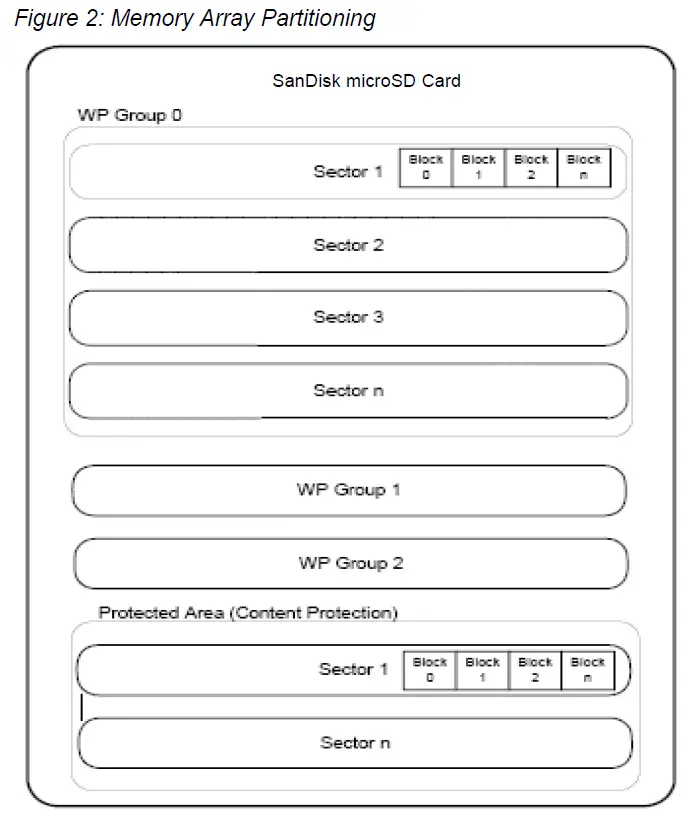
Figure 1-3 illustrates the formatting of a data transfer.
Figure 3: Data Transfer Formats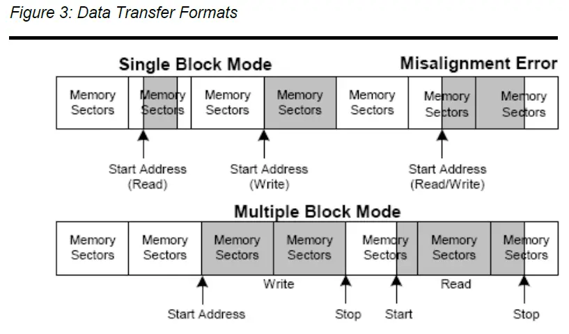
Table 5 contains descriptions for each transfer mode.
Table 5
Table 1-1 Mode Definitions
| Mode | Description |
|
Single Block | In this mode the host reads or writes one data block in a pre-specified length. The data block transmission is protected with 16-bit CRC that is generated by the sending unit and checked by the receiving unit. The block length for read operations is limited by the device sector size (512 bytes) but can be as small as a single byte. Misalignment is not allowed. Every data block must be contained in a single physical sector. The block length for write operations must be identical to the sector size and the start address aligned to a sector boundary. |
|
Multiple Block | This mode is similar to the single block mode, except for the host can read/ write multiple data blocks (all have the same length) that are stored or retrieved from contiguous memory addresses starting at the address specified in the command. The operation is terminated with a stop transmission command. Misalignment and block length restrictions apply to multiple blocks and are identical to the single block read/write operations. |
SPI Mode
The SPI Mode is a secondary communication protocol for the SanDisk Industrial microSD card. This mode is a subset of the SD Protocol, designed to communicate with an SPI channel, commonly found in Motorola and other vendors’ microcontrollers. Detailed information about SPI Mode can be found in Section 7 or the SDA Physical Layer Specification, Version 3.01.
PRODUCT SPECIFICATIONS
microSD Card
This section provides product specifications for the SanDisk Industrial microSD Card.
Typical Card Power Requirements
The values stated in Table 6 represent the SanDisk SD Card power requirements.
Table 6
| Mode | Maximum Value | Typical Value at 25C |
| Standard Mode (25 MHz) | ||
| Sleep | 500 uA | |
| Read | 100 mA | |
| Write | 100 mA | |
| Standard Mode – for SDXC card – Host selected XPC bit in XPC bit on(25 MHz) ACMD41 | ||
| Sleep | 500 uA | |
| Read | 150 mA | |
| Write | 150 mA | |
| High Performance Mode (50 MHz) | ||
| Sleep | 500 uA | |
| Read | 200 mA | |
| Write | 200 mA | |
| UHS-I SDR50 Mode – (100 MHz) | ||
| Sleep | 500 uA | |
| Read | 400 mA | |
| Write | 400 mA | |
| UHS-I DDR50 Mode – (50 MHz) | ||
| Sleep | 500 uA | |
| Read | 400 mA | |
| Write | 400 mA | |
NOTE Current consumption is measured by averaging over one (1) second. Refer to Section 6.6.3 of the SDA Physical Layer Specification, Version 3.01 for more information.
System Performance
This section provides the system performance specifications for the SanDisk Industrial microSD Card. All performance values in Table 2-2 were measured under the following conditions:
- Voltage range 2.7 to 3.6V
- Operating temperature
- -25° C to 85° C for wide temperature range Industrial Cards.
- Independent of card clock frequency
Table 7
System Performance
| Timing | Maximum Value |
| Block Read Access Time | 100 ms |
| Block Write Access Time | 250 ms for SDHC, 500 ms for SDXC |
| ACMD41 to ready after power-up | 1s |
Table 8
| Capacity in GB3 | 8GB | 16GB | 32GB | 64GB |
| Endurance4 [TBW] | 16 | 32 | 96 | 192 |
Table 9
| Capacity in GB1 | 8GB, 16GB | 32GB, 64GB |
| Speed Class | 10 | 10 |
| Sequential Read (MB/s) | 40 | 20 |
| Sequential Write (MB/s) | 10 | 20 |
Physical Specifications
For detail dimensions and tolerances refer to SDA microSD Card specification.
INTERFACE DESCRIPTION
Pins and Registers
The SanDisk Industrial microSD Card has exposed contacts on one side. The host uses a dedicated 9-pin connector to connect to SD cards.
In Table 3-1, pin assignments for the SanDisk microSD Card are for SD Bus Mode. Table 3-2 contains pin assignments for SPI Mode.
NOTE Pin assignments are provided by the SDA Physical Layer Specification, Version 3.00 and associated addendums. For more details, refer to Section 3.7 of the SDA Physical Layer Specification Layer 3.00.
Table 3-1 SD Bus Mode Pin Assignment
| Pin No. | Name | Typea | Description |
| SD Card | |||
| 1 | CD/DAT3b | I/Oc/PP | Card Detect/Data Line [bit 3] |
| 2 | CMD | PP | Command/Response |
| 3 | VSS1 | S | Supply Voltage Ground |
| 4 | VDD | S | Supply Voltage |
| 5 | CLK | I | Clock |
| 6 | VSS2 | S | Supply Voltage Ground |
| 7 | DAT0 | I/O/PP | Data Line [bit 0] |
| 8 | DAT1 | I/O/PP | Data Line [bit 1] |
| 9 | DAT2 | I/O/PP | Data Line [bit 2] |
a. Type Key: S=power supply; I= input; O=output using push-pull drivers; PP=I/O using push-pull drivers.
b. The extended DAT lines (DAT1-DAT3) are input on power up. They start to operate as DAT lines after the SET_BUS_WIDTH Type Key: S=power supply; I=input; O=output using push-pull drivers; PP=I/O using push-pull drivers.
c. At power up this line has a 50 kilohm pull-up enabled in the card. This resistor serves two functions: Card detection and Mode Selection. For Mode Selection, the host can drive the line high or let it be pulled high to select SD mode. If the host wants to select SPI mode it should drive the line low. For Card detection, the host detects that the line is pulled high. This pull-up should be disconnected by the user, during regular data transfer, with SET_CLR_CARD_DETECT (ACMD42) command.
The SanDisk microSD Card pin assignments in Table 3-2 below are for SPI Mode.
Table 10
SPI Mode Pin Assignment
| Pin No. | Name | Type | Description |
| SD Card | |||
| 1 | CS | I | Chip Select (active low) |
| Pin No. | Name | Type | Description |
| 2 | DataIn | I | Host-to-Card Commands and Data |
| 3 | VSS1 | S | Supply Voltage Ground |
| 4 | VDD | S | Supply Voltage |
| 5 | SCLK | I | Clock |
| 6 | VSS2 | S | Supply Voltage Ground |
| 7 | DataOut | O/PP | Card-to-Host Data and Status |
| 8 | RSV | — | Reserved |
| 9 | RSV | — | Reserved |
Each card has a set of information registers. Register descriptions and SDA references are provided in Section 3.7 of the SDA Physical Layer Specification, Version 3.00.
Table 11
microSD Card Register Overview
| Register Abbreviation | Width (in bits) | Register Name |
| CID | 128 | Card Identification Number |
| RCA | 16 | Relative Card Address |
| CSD | 128 | Card Specific Data |
| SCR | 64 | SD Configuration Register |
| OCR | 32 | Operation Condition Register |
| SSR | 512 | SD Status Register |
| CSR | 32 | Card Status Register |
Bus Topology
The family of SanDisk Industrial microSD products supports two communication protocols: SD and SPI. For more details, refer to Section 3.5 of the SDA Physical Layer Specification, Version 3.01. Section 6 of the specification contains a bus circuitry diagram for reference.
- SD Bus
For more details, refer to Section 3.5.1 of the SDA Physical Layer Specification, Version 3.01. - SPI Bus
For more details, refer to Section 3.5.2 of the SDA Physical Layer Specification, Version 3.01.
Hot Insertion and Power Protection
Refer to Section 6.1, 6.2 and 6.3 of the SDA Physical Layer Specification, Version 3.01.
Electrical Interface
The power scheme of SanDisk Industrial microSD products is handled locally in each card and in the bus master. Refer to Section 6.4 of the SDA Physical Layer Specification, Version 3.01.
Power Up
Power must be applied to the VDD pin before any I/O pin is set to logic HIGH. In other words, CMD, CLK, and DAT0-3 must be at zero (0) volts when power is applied to the VDD pin. For more information, refer to Section 6.4.1 of the SDA Physical Layer Specification, Version 3.01.
Figure 4 provides the recommended power control scheme
Figure 4: Recommended Power Control Scheme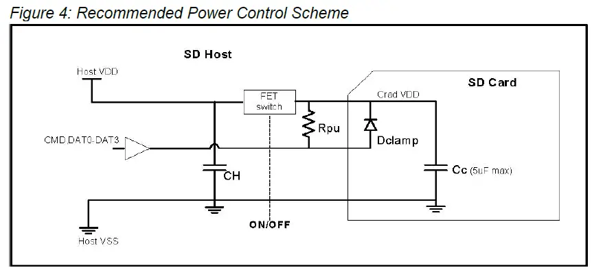
The recommended power control scheme for SanDisk microSD card is illustrated in Figure 3-1. Most card connectors have a card detect switch that signals the SD host when the card is inserted. After the host is aware of the card insertion, it turns on the FET switch to apply power to card’s VDD pin.
Once the card is inserted and all card pins are making contact, there is a delay before the FET switch is turned on.
IMPORTANT: Because there are clamping diodes on the CMD, CLK, and DAT0-3 pins, it is crucial to ensure that CLK, CMD, and DAT0-3 are at zero (0) volts during the delay and before the FET switch is turned on. If any I/O pin, (CMD, CLK, or DAT0-3) goes above zero volts during the delay and before power reaches the card VDD pin, it will forward bias the clamping diodes and can cause the card to go into an unknown state.
It is the host’s responsibility to make sure power gets to VDD before CMD, CLK, or DAT0-3 go above zero volts.
Bus Operating Conditions
SPI Mode bus operating conditions are identical to SD Card Bus Mode operating conditions. For details, see Section 6.6 of the SDA Physical Layer Specification, Version 3.01.
Bus Timing (Standard Mode)
See Section 6.7 of the SDA Physical Layer Specification, Version 3.01.
microSD Card Registers
There is a set of eight registers within the card interface. However, the DSR Register is optional and is not used in SanDisk Industrial microSD Card. For specific information about all registers, refer to Section 5 of the SDA Physical Layer Specification, Version 3.01.
- Operation Conditions Register
The Operation Conditions Register (OCR) stores a card’s VDD voltage profile. Refer to Section 5.1 of the SDA Physical Layer Specification, Version 3.01 for more information. - Card Identification Register
The Card Identification (CID) Register is 16 bytes long and contains the unique card identification number. It is programmed during card manufacturing and cannot be changed by card hosts. See Table 3-4.
Table 12
CID Register Definitions
| Name | Type | Width | CID Value | Comments | ||||||||||
| Manufacturer ID (MID) |
Binary |
8 |
0x03 | Manufacturer IDs are controlled and assigned by the SD-3C, LLC. | ||||||||||
|
OEM/ Application ID (OID) |
ASCII |
16 |
SD ASCII Code 0x53, 0x44 | Identifies the card OEM and/or the card contents. The OID is controlled and assigned by the SD-3C, LLC. | ||||||||||
|
Product Name (PNM) |
ASCII |
40 |
|
Five-character ASCII string. | ||||||||||
| Product Revision (PRV) |
BCD |
8 |
Product Revision xx | See Section 5.2 in the SDA Physical Layer Specification, Version 3.00. |
| Name | Type | Width | CID Value | Comments |
| Serial Number (PSN) | Binary | 32 | Product Serial Number | 32-bit unsigned integer |
| Reserved | — | 4 | — | — |
| Manufacture Date Code (MDT) | BCD | 12 | Manufacture date (for example, April 2001=0x014) | Manufacturing date–yym (offset from 2000) |
| CRC7 Checksum (CRC) | Binary | 7 | CRC7 | Calculated |
| Not used, always 0 | — | 1 | — | — |
Card Specific Data Register
The Card Specific Data (CSD) Register configuration information is required to access card data. The CSD defines the data format, error correction type, maximum data access time, etc. The field structures of the CSD Register vary depending on the physical specifications and card capacity. The CSD_STRUCTURE field in the CSD Register indicates which structure version is used. Table 3-5 shows the version number as it relates to the CSD structure. Refer to Section 5.3.1 of the SDA Physical Layer Specification, Version 3.01 for more information.
Table 13
CSD Register Structure
| CSD_STRUCTURE | CSD Structure Version | Valid for SD Card Physical Specification Version / Card Capacity |
| 0 | CSD Version 1.0 | Version 1.01 to 1.10 Version 2.00/Standard Capacity |
| 1 | CSD Version 2.0 | Version 2.00/High Capacity |
| 2-3 | Reserved | — |
Table 3-6 provides an overview of the CSD Register. More field-specific information can be found in Section 5.3.2 of the SDA Physical Layer Specification, Version 3.01.
Table 14
CSD Register (CSD Version 1.0)
| Field | CSD Value | Description |
| CSD_STRUCTURE | 1.0 | CSD structure |
| — | — | Reserved |
| TAAC | 1.5 msec | Data read access-time-1 |
| NSAC | 0 | Data read access-time-2 in CLK cycles (NSAC*100) |
| TRANS_SPEED | Standard Mode 25 MHz High Performance Mode 50 MHz Ultra High Speed Mode 100 MHz | Maximum data transfer rate |
| CCC | All (inc. WP, lock/unlock) | Card command classes |
| READ_BL_LEN | 2G = 0xA Up to 1G = 0x9 | Maximum read data block length |
| READ_BL_PARTIAL | Yes | Partial blocks for read allowed |
| WRITE_BLK_MISALIGN | No | Write block misalignment |
| READ_BLK_MISALIGN | No | Read block misalignment |
| DSR_IMP | No | DSR implemented |
| — | — | Reserved |
| C_SIZE 64 MB 128 MB 256 MB 512 MB 1 GB 2 GB | Secured 0xEDF 0xF03 0xF13 0xF1E 0xF22 0xF24 | Device Size |
| VDD_R_CURR_MIN | 100 mA | Maximum read current @VDD min |
| VDD_R_CURR_MAX | 80 mA | Maximum read current @VDD max |
| VDD_W_CURR_MIN | 100 mA | Maximum write current @VDD min |
| VDD_W_CURR_MAX | 80 mA | Maximum write current @VDD max |
| C_SIZE_MULT | 2G=2048 1G=1024 512=512 256=256 128=128 64=64 | Device size multiplier |
| ERASE_BLK_EN | Yes | Erase single block enable |
| SECTOR_SIZE | 31 blocks | Erase sector size |
| WP_GRP_SIZE | 127 sectors | Write protect group size |
| WP_GRP_ENABLE | Yes | Write protect group enable |
| Reserved | — | Reserved for MMC compatibility |
| R2W_FACTOR | x16 | Write speed factor |
| WRITE_BL_LEN | 0x9 | Maximum write data block length |
| WRITE_BL_PARTIAL | No | Partial blocks for write allowed |
| — | — | Reserved |
| FILE_FORMAT_GRP | 0 | File format group |
| COPY | Has been copied | Copy flag (OTP) |
| PERM_WRITE_PROTECT | Not protected | Permanent write protection |
| TMP_WRITE_PROTECT | Not protected | Temporary write protection |
| FILE_FORMAT | HD w/partition | File format |
| Reserved | — | Reserved |
| Field | CSD Value | Description |
| CRC | CRC7 | CRC |
| — | — | Not used, always “1” |
Refer to Section 5.3.3, Table 5-16 of the SDA Physical Layer Specification, Version 3.00 for more detailed information.
Table 15
CSD Register (CSD Version 2.0)
| Field | CSD Value | Description |
| CSD_STRUCTURE | 2.0 | CSD structure |
| — | — | Reserved |
| TAAC | 1.5 msec | Data read access-time |
| NSAC | 0 | Data read access-time in CLK cycles (NSAC*100) |
| TRANS_SPEED | Standard Mode 25 MHz High Performance Mode 50 MHz Ultra High Speed Mode 100 MHz | Maximum data transfer rate |
| CCC | All (inc. WP, lock/unlock) | Card command classes |
| READ_BL_LEN | 9 | Maximum read data block length |
| READ_BL_PARTIAL | Yes | Partial blocks for read allowed |
| WRITE_BLK_MISALIGN | No | Write block misalignment |
| READ_BLK_MISALIGN | No | Read block misalignment |
| DSR_IMP | No | DSR implemented |
| — | 0 | Reserved |
| C_SIZE 4 GB 6 GB 8 GB 12 GB 16 GB 32 GB | Secured 0x1E5C 0x2D8C 0x3CDC 0x5B6C 0x79FC 0xF45C | Device Size |
| — | 0 | Reserved |
| ERASE_BLK_EN | 1 | Erase single block enable |
| SECTOR_SIZE | 64 blocks | Erase sector size |
| WP_GRP_SIZE | 000000b | Write protect group size |
| WP_GRP_ENABLE | No | Write protect group enable |
| Reserved | — | Reserved for MMC compatibility |
| R2W_FACTOR | x4 | Write speed factor |
| WRITE_BL_LEN | Maximum write data block length | |
| WRITE_BL_PARTIAL | No | Partial blocks for write allowed |
| — | — | Reserved |
| FILE_FORMAT_GRP | 0 | File format group |
| COPY | Has been copied | Copy flag (OTP) |
| PERM_WRITE_PROTECT | Not protected | Permanent write protection |
| TMP_WRITE_PROTECT | Not protected | Temporary write protection |
| FILE_FORMAT | HD w/partition | File format |
| Reserved | — | Reserved |
| Field | CSD Value | Description |
| CRC | CRC7 | CRC |
| — | — | Not used, always “1” |
Card Status Register
The Card Status Register (CSR) transmits the card’s status information (which may be stored in a local status register) to the host. The CSR is defined in Section 4.10.1 in the SDA Physical Layer Specification, Version 3.01.
microSD Status Register
The microSD Status Register (SSR) contains status bits that are related to the SD Card proprietary features and may be used for future applications. The SD Status structure is described in Section 4.10.2 in the SDA Physical Layer Specification, Version 3.01.
Relative Card Address Register
The 16-bit Relative Card Address (RCA) Register carries the card address published by the card during the card identification. Refer to Section 5.4 in the SDA Physical Layer Specification, Version 3.01 for more information.
microSD Card Configuration Register
The microSD Card Configuration Register (SCR) is in addition to the CSD Register. The SCR provides information about special features in the SanDisk SD Card products. For more information, refer to Section 5.6 in the SDA Physical Layer Specification, Version 3.01.
microSD Card Registers in SPI Mode
All card registers are accessible in SPI Mode. Their format is identical to the format in the SD Bus Mode. However, a few fields are irrelevant in SPI Mode. In SPI Mode: The Card Status Register has a different, shorter, format as well. Refer to Section 7.4 in the SDA Physical Layer Specification, Version 3.01 for more details.
Data Interchange Format and Card Sizes
In general, a file system provides a structure for data in SanDisk microSD Card products. The SD Card File System Specification, published by the SDA, describes the file format system that is implemented in the SanDisk microSD Card products. In general, each card is divided into two separate DOS-formatted partitions as follows:
- User Area–used for secured and non-secured data storage and can be accessed by the user with regular read/write commands.
- Security Protected Area–used by content protection applications to save security-related data and can be accessed by the host using the secured
read/write command after doing authentication as defined in the SD Security Specification. The security-protected area size is defined by SanDisk as approximately one percent of the total size of the card.
Table 3-8 describes the user area for SanDisk SD Card.
Table 16
User Data Bytes
| Capacity5 | User Data Bytes6 |
| 64GB | 63,831,015,424 |
| 32GB | 31,902,400,512 |
| 16GB | 15,923,150,848 |
| 8GB | 7,939,817,472 |
MICRO SD CARD PROTOCOL DESCRIPTION
General Description
SD Protocol information for the SanDisk Industrial microSD Card is contained in this chapter; information includes SD bus protocol, card identification, and a functional description.
SD Bus Protocol
Communication over the SD bus is based on command and data-bit streams initiated by a start bit and terminated by a stop bit. See Section 3.6.1 of the SDA Physical Layer Specification, Version 3.01 for details.
Functional Description
The host controls all communication between itself and the cards. To demonstrate how this communication works, this section provides a general overview of the card identification and data transfer modes; commands; card dependencies; various card operation modes and restrictions for controlling the clock signal. All microSD Card commands, together with corresponding responses, state transitions, error conditions, and timings are also provided. For detailed information, refer to Section 4 of the SDA Physical Layer Specification, Version 3.01.
Card Identification Mode
In Card Identification Mode, the host resets all cards, validates operation voltage range, identifies and requests cards to publish a relative card address. For more information see Section 4.2 in the SDA Physical Layer Specification, Version 3.01.
Data Transfer Mode
In Data Transfer Mode, the host may operate the SanDisk Industrial microSD Card in the fPP frequency range. In the SDA Physical Specification, this section includes information about data read and write, erase, write-protect management, card lock/unlock operations, application-specific commands, switch function command, high-speed mode, command system, and the Send Interface Condition command (CMD8). CMD8 is part of identification mode and command functional differences in high capacity SD cards. For more detailed information, refer to Section 4.3 of the SDA Physical Layer Specification, Version 3.01.
Clock Control
The host can use the bus clock signal in SanDisk Industrial microSD cards to switch them to energy saving mode or to control data flow on the bus. See Section 4.4 of the SDA Physical Layer Specification, Version 3.01.
Cyclic Redundancy Codes
The Cyclic Redundancy Check (CRC) protects against transmission errors that may occur on the bus in SanDisk SD Cards. Detailed information and examples for CRC7 and CRC16 are provided in Section 4.5 of the SDA Physical Layer Specification, Version 3.01.
Error Conditions
See Section 4.6 of the SDA Physical Layer Specification, Version 3.01.
Commands
See Section 4.7 of the SDA Physical Layer Specification, Version 3.01 for detailed information about card commands in the SanDisk SD Card.
Card State Transition
In microSD cards, the state transition is dependent on the received command. The transition is defined in Section 4.8 of the SDA Physical Layer Specification, Version 3.01 along with responses sent on the command line.
Timing Diagrams and Values
See Section 4.12 of the SDA Physical Layer Specification, Version 3.01.
Speed Class Specification
The speed class specification classifies card performance by speed class number and offers a method to calculate performance. For more information, refer to Section 4.13 of the SDA Physical Layer Specification, Version 3.01.
Erase Timeout Calculation
See Section 4.14 of the SDA Physical Layer Specification, Version 3.01.
MARKING
Figure 5: Marking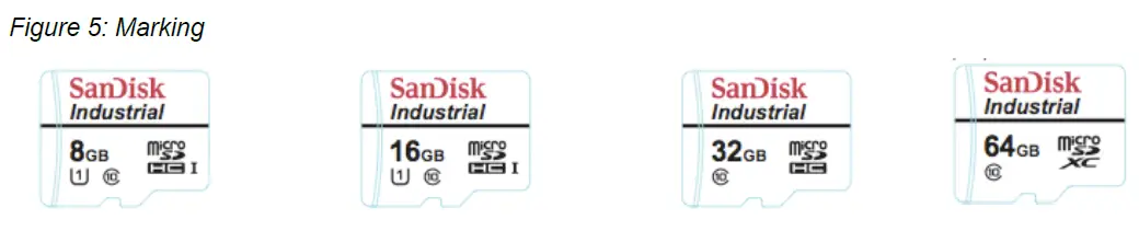
ORDERING INFORMATION
Table 17
| Capacity | Part Numbers |
| 8 GB | SDSDQAF-008G-I |
| 16 GB | SDSDQAF-016G-I |
| 32 GB | SDSDQAF2-032G-I |
| 64 GB | SDSDQAF2-064G-I |
HOW TO CONTACT US
SanDisk Corporation, Corporate Headquarters.
951 SanDisk Dr.
Milpitas, CA 95035-7933 Phone: +1-408-801-1000 www.sandisk.com
Please refer to the SanDisk website for contact information: www.sandisk.com
Download PDF: SanDisk industrial micro SD Card User Manual


