![]() SMC0430B-800480 Series
SMC0430B-800480 Series
MCU Interface IPS LCD Module USER MANUAL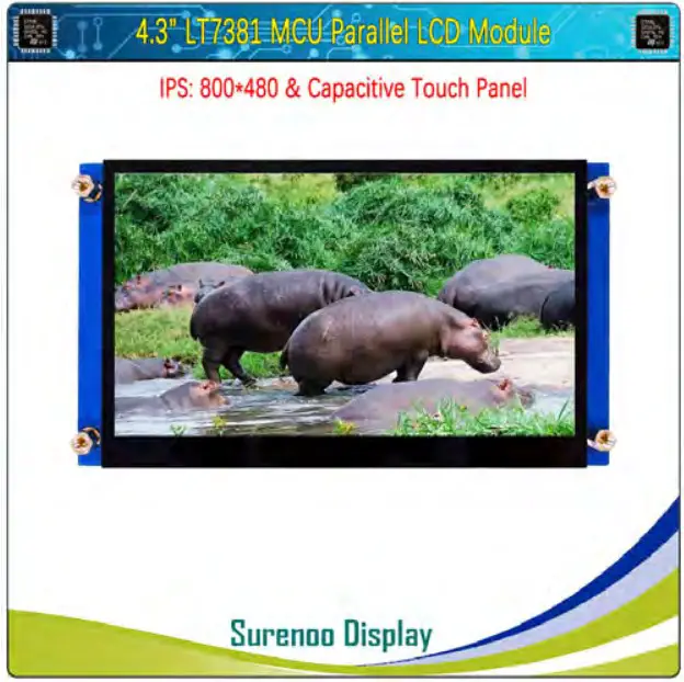 Model No.: SMC0430B-800480
Please click the following image to buy the sample
GENERAL INFORMATION
| Item of general information | Contents | Unit | |
| LCD Display Size (Diagonal) | 4.3 | inch | |
| Module Structure | LCD Display + CTP Touch + PCB | – | |
| LCD Display Type | TFT/TRANSMISSIVE | – | |
| LCD Display Mode | Normally Black | – | |
| Recommended Viewing Direction | ALL | o’clock | |
| Gray inversion Direction | o’clock | ||
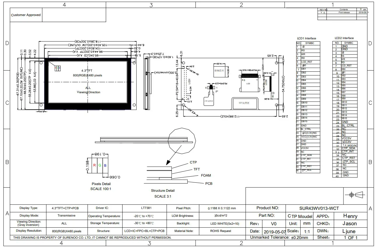
| Module size (W×H×T) | 118.28×67.31×7.25 | mm | |
| Active area (W×H) | 95.04×53.68 | mm | |
| Number of pixels (Resolution) | 800RGB×480 | pixel | |
| Pixel pitch (W×H) | 0.1188×0.1122 | mm | |
| LCD Driver IC | – | – | |
| Module Interface Type | LCD | MCU 16bit/8bit interface | – |
| CTP | IIC interface | – | |
| Module Input voltage | 5.0V or 3.3V | V | |
| Module Power consumption | – | mW | |
| Color Numbers | 16.7M | – | |
| Backlight Type | White LED | – | |
| LCM Controller | LT7381 | – | |
ABSOLUTE MAXIMUM RATINGS
| Parameter of absolute maximum ratings | Symbol | Min | Max | Unit |
| Operating temperature | Top | -20 | 70 | ℃ |
| Storage temperature | TSgt | -30 | 80 | ℃ |
| Humidity | RH | – | 90%(Max 60℃) | RH |
Note: Absolute maximum ratings means the product can withstand short-term, not more than 120 hours. If the product is a long time to withstand these conditions, the life time would be shorter.
ELECTRICAL CHARACTERISTICS(DC CHARACTERISTICS)
| Parameter of DC characteristics | Symbol | Min. | Typ. | Max. | Unit |
| PCB operating voltage | VCC5V | – | 5.0 | – | V |
| LCD I/O operating voltage | VDD | 3.0 | 3.3 | 3.6 | V |
| Input voltage ‘H’ level | VIH | 2 | – | 3.6 | V |
| Input voltage ‘L’ level | VIL | -0.3 | – | 0.8 | V |
| Output voltage ‘H’ level | VOH | 2.4 | – | – | V |
| Output voltage ‘L’ level | VOL | – | – | 0.4 | V |
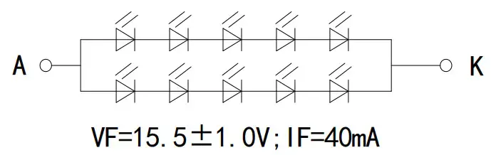
BACKLIGHT CHARACTERISTICS
| Item of backlight characteristics | Symbol | Min. | Typ. | Max. | Unit | Remark |
| Forward Voltage | If | 14 | 15.5 | 16.5 | V | Note1 |
| Forward Current | If | – | 40 | – | mA | – |
| Number of LED | – | – | 5*2 | – | Piece | – |
| LED Connection mode | P/S | – | 5S*2P | – | – | – |
| Lifetime of LED | – | – | 10000 | – | hour | Note2 |
Note:
- Note1: The LED Supply Voltage is defined by the number of LED at Ta=25℃ and If=40mA.
- Note2: The LED lifetime define as the estimated time to 50% degradation of initial luminous. The LED lifetime could be decreased if operating If is larger than 20mA.
- Backlight circuit:
ELECTRO-OPTICAL CHARACTERISTICS
| Item of electro-optical characteristics | Symbol | Condition | Min. | Typ. | Max. | Unit | Remark | Note | |
| Response time | Tr+Tf | θ=0 =0 Ta=25℃ | – | 30 | 40 | ms | FIG 1. | 4 | |
| Contrast Ratio | CR | 640 | 800 | – | – | FIG 2. | 1 | ||
| Luminance uniformity | WHITE | – | 80 | – | % | FIG 2. | 3 | ||
| Surface Luminance | Lv | – | 350 | – | cd/m2 | FIG 2. | 2 | ||
| CIE (x, y) chromaticity | White | White x | θ=0 =0 Ta=25℃ | 0.309 | 0.313 | 0.315 | – | FIG 2. | 5 |
| White y | 0.337 | 0.339 | 0.341 | ||||||
| Red | Red x | 0.629 | 0.631 | 0.633 | |||||
| Red y | 0.327 | 0.329 | 0.331 | ||||||
| Green | Green x | 0.326 | 0.328 | 0.330 | |||||
| Green y | 0.546 | 0.548 | 0.550 | ||||||
| Blue | Blue x | 0.134 | 0.136 | 0.138 | |||||
| Blue y | 0.139 | 0.141 | 0.143 | ||||||
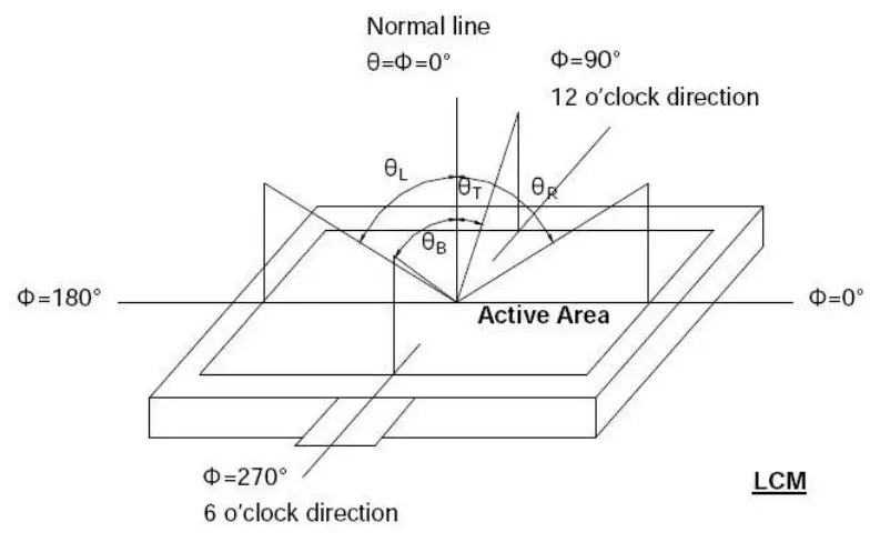
| Viewing angle range | =90(12 o’clock) | CR 10 | 70 | 80 | – | deg | FIG 3. | 6 | |
| =270(6 o’clock) | 70 | 80 | – | deg | |||||
| =0(3 o’clock) | 70 | 80 | – | deg | |||||
| =180(9 o’clock) | 70 | 80 | – | deg | |||||
| NTSC ratio | – | – | – | 50 | – | % | – | – | |
Note 1. Contrast Ratio (CR) is defined mathematically by the following formula. For more information see FIG 2.:  Note 2. Surface luminance is the LCD surface from the surface with all pixels displaying white. For more information see FIG 2.
Lb=Average Surface Luminance with all white pixels (P1,P2,P3,P4,P5,P6,P7,P8,P9)
Note 3. The uniformity in surface luminance Whitelist determined by measuring
Note 3. The uniformity in surface luminance WHITE is determined by measuring luminance at each test position 1 through 9, and then dividing the maximum luminance of 9points luminance by minimum luminance of 9 points luminance. For more information see FIG 2.

Note 4. Response time is the time required for the display to transition from White to black(Rise Time, Tr) and from black to white(Decay Time, Tf). For additional information see FIG 1.
Note 5. CIE (x, y) chromaticity ,The x,y value is determined by screen active area position 5.
For more information see FIG 2.
Note 6. Viewing angle is the angle at which the contrast ratio is greater than a specific value.
For TFT module, the specific value of contrast ratio is 10.The angles are determined for the horizontal or x axis and the vertical or y axis with respect to the z axis which is normal to the LCD surface. For more information see FIG 3.
Note 7. For Viewing angle and response time testing, the testing data is base on Autronic-Melchers’s ConoScope. Series Instruments. For contrast ratio, Surface Luminance,
Luminance uniformity and CIE,the testing data is base on BM-7 photo detector.
Note 8. For TN type TFT transmissive module, Gray scale reverse occurs in the direction of panel viewing angle.
FIG.1. The definition of Response Time
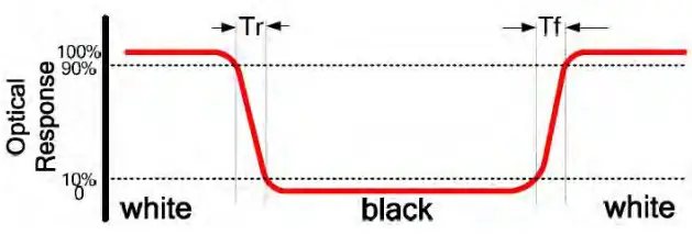
FIG.2. Measuring method for Contrast ratio, surface luminance, Luminance uniformity, CIE (x , y) chromaticity
A : H/6 ;
B : V/6 ;
H,V : Active Area(AA) size
Measurement instrument: BM-7; Light spot size=5mm, 350mm distance from the LCD surface to detector lens.

FIG.3. The definition of viewing angle
INTERFACE DESCRIPTION
LCD1 Interface Description
| NO. | Symbol | I/O | DESCRIPTION |
| 1 | CS | I | Chip select |
| 2 | RS | I | Data/Command select |
| 3 | WR | I | Write strobe signal |
| 4 | RD | I | Read strobe signal |
| 5 | RST | I | LCD RESET signal, Low is active |
| 6~21 | DB0~ DB15 | I/O | Data bus(D0:LSB; D15:MSB) |
| 22 | GND | Power supply | Power ground |
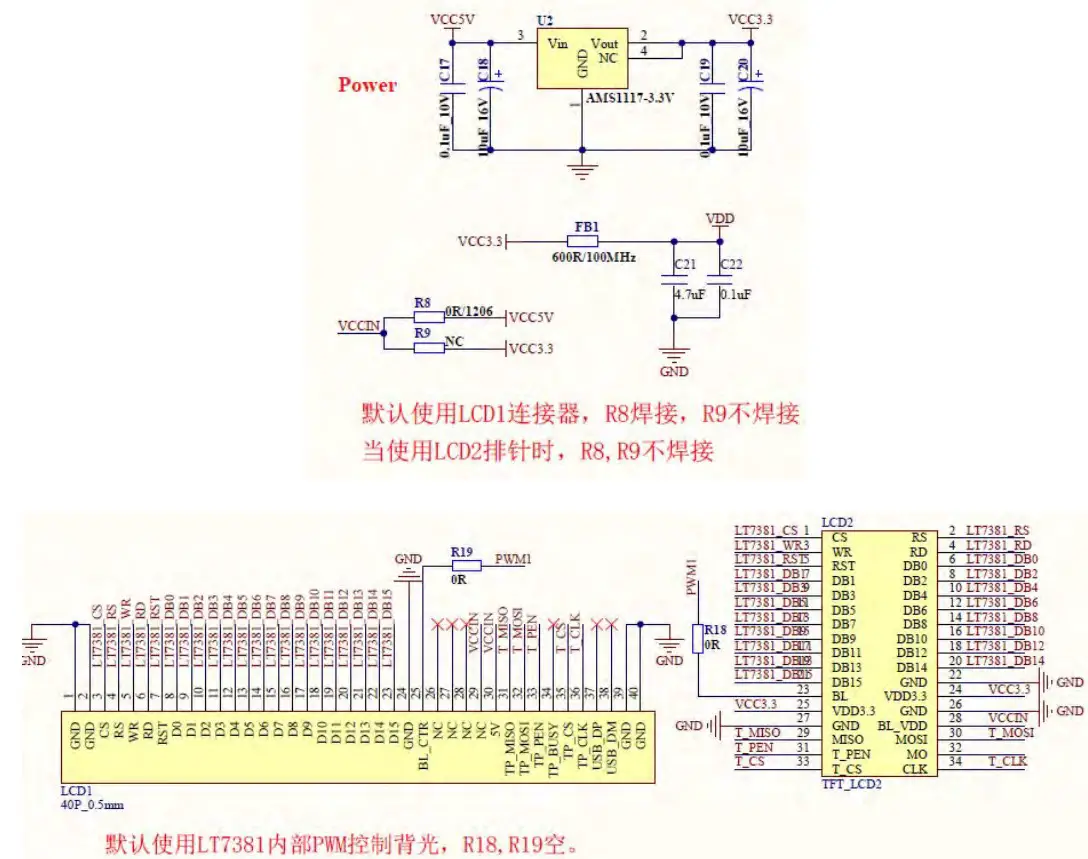
| 23 | BL_CTRL | I | Backlight control pin |
| 24~25 | VCC(3.3V) | Power supply | Module Power input(3.3V Typ.) (*note1) |
| 26~27 | GND | Power supply | Power ground |
| 28 | VDD5V | Power supply | Module Power input (5V Typ.) (*note1) |
| 29 | NC | O | RTP Serial Data Output |
| 30 | CTP_SDA | I | TP Serial Data Input |
| 31 | CTP_INT | I | TP INT Interrupt Output |
| 32 | NC | – | No connection |
| 33 | CTP_RST | I | TP Chip reset pin |
| 34 | CTP_SCL | I | TP Clock Input |
LCD2 Interface Description
| NO. | Symbol | I/O | DESCRIPTION |
| 1~2 | GND | Power supply | Power ground |
| 3 | CS | I | Chip select |
| 4 | RS | I | Data/Command select |
| 5 | WR | I | Write strobe signal |
| 6 | RD | I | Read strobe signal |
| 7 | RST | I | LCD RESET signal, Low is active |
| 8~23 | DB0~DB15 | I/O | Data bus(D0:LSB; D15:MSB) |
| 24 | GND | Power supply | Power ground |
| 25 | BL_CTRL | I | Backlight control pin |
| 26~28 | NC | – | No connection |
| 29~30 | VDD5V | Power supply | Module Power input (5V Typ.) (*note1) |
| 31 | TP_MISO/NC | O | No connection |
| 32 | CTP_SDA | I | TP Serial Data Input |
| 33 | CTP_INT | I | TP INT Interrupt Output |
| 34 | NC | – | No connection |
| 35 | CTP_RST | I | TP Chip reset pin |
| 36 | CTP_SCL | I | TP Clock Input |
| 37 | NC | I | No connection |
| 38 | NC | I | No connection |
| 39~40 | NC | – | No connection |
Note1:
Power supply of module ,when used for LCD1 and LCD2 interface , The following instructions:
a The power input pin is used for LCD1,R2 should be removed on the PCB.
b The power input pin is used for LCD1 and used for VCC3.3 power pins only,R2 should be removed and R4 should be used on the PCB.
INPUT TIMING
8080 Parallel Mode Interface Timing
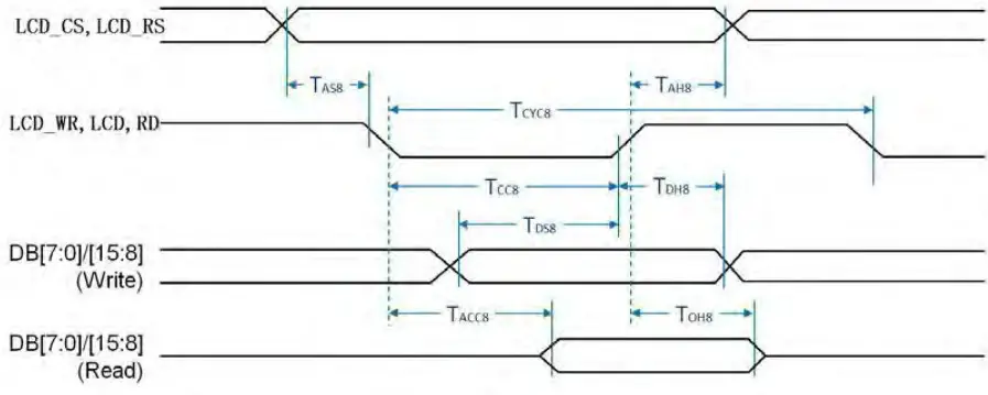
| Symbol | Parameter | Rating | Unit | Note | |
| Min. | Max. | ||||
| TCYC8 | Cycle Time | 50 | — | ns | tic is one system clock period: tic = 1/SYS_CLK |
| TCC8 | Strobe Pulse Width | 20 | — | ns | |
| TAS8 | Address Setup Time | 0 | — | ns | |
| TAH8 | Address Hold Time | 10 | — | ns | |
| TDS8 | Data Setup Time | 20 | — | ns | |
| TDH8 | Data Hold Time | 10 | — | ns | |
| TACC8 | Data Output Access Time | 0 | 20 | ns | |
| TOH8 | Data Output Hold Time | 0 | 20 | ns | |
Register Write:
- Address Write: Write the Register’s Address. For example, 00h i.e. REG[00h], 01h i.e. REG[01h], 02h i.e. REG[02h] ……
- Data Write: Write Data to the Register
Register Read:
- Address Write: Write the Register’s Address
- Data Write: Read Data from the Register
Displays Memory (Display RAM) is where the TFT screen image data is stored,. Host through interface and write data into Display RAM. The procedure of access Display RAM is as following:
Display RAM Write:
- Set the Active Window Registers before writing any image data.
- Perform an register write to Graphic R/W Position Register 0, REG[5Fh]).
- Repeat step 2 until setup all the Active Window & Graphic R/W Position Coordinates.
- Perform an address write to point to Memory Data Port Register (REG[04h])
- Perform data writes to fill the window. Each write to the Memory Data Port will auto-increment the internal memory address.
RELIABILITY TEST CONDITIONS
| No. | Test Item | Test Condition |
| 1 | High Temperature Storage | 80℃/120 hours |
| 2 | Low Temperature Storage | -30℃/120 hours |
| 3 | High Temperature Operating | 70℃/120 hours |
| 4 | Low Temperature Operating | -20℃/120 hours |
| 5 | Temperature Cycle Storage | -20℃(30min.)~25(5min.)~70℃(30min.)×10cycles |
A Inspection after test:
Inspection after 2~4 hours storage at room temperature, the sample shall be free from defects:
- Air bubble in the LCD;
- Selleck; Non-display;
- Missing segments;
- Glass crack;
- Current is twice higher than initial value.
Premark:
- The test samples should be applied to only one test item.
- Sample size for each test item is 5~10pcs.
- Failure Judgment Criterion: Basic Specification, Electrical Characteristic, Mechanical
Characteristic, Optical Characteristic.
INSPECTION CRITERION
This specification is made to be used as the standard of acceptance/rejection criteria for TFT-LCD/IPS TFT-LCD module product, and this specification is applicable only in the case that the size of module equal to or exceed than 3.5 inch.
10.1 Sample plan
Sampling plan according to GB/T2828.1-2003/ISO 2859-1:1999 and ANSI/ASQC Z1.4-1993,normal level 2 and based on:
Major defect: AQL 0.65
Minor defect: AQL 1.5
10.2 Inspection condition
Viewing distance for cosmetic inspection is about 30cm with bare eyes, and under an environment of 20~40W light intensity, all directions for inspecting the sample should be within 45°against perpendicular line. (Normal temperature 20~25℃and normal humidity 60 ±15%RH )
10.3 Definition of Inspection Item.
A Definition of inspection zone in LCD.
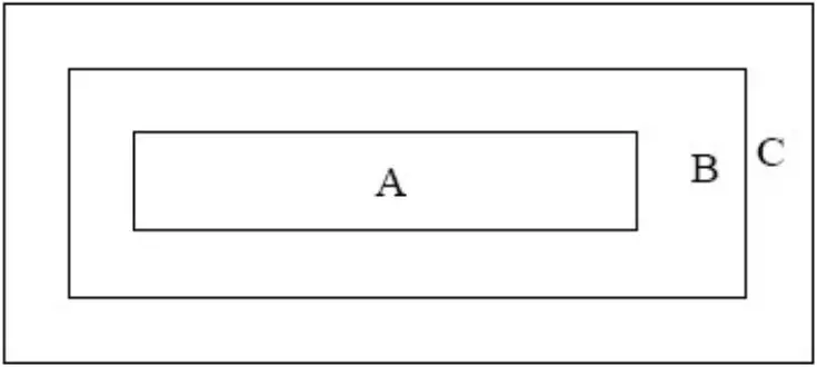
Zone A: character/Digit area
Zone B: viewing area except Zone A (Zone A + Zone B=minimum Viewing area)
Zone C: Outside viewing area (invisible area after assembly in customer’s product)
Fig.1 Inspection zones in an LCD
Note: As a general rule, visual defects in Zone C are permissible, when it is no trouble for quality and assembly of customer’s product.
B Definition of some visual defect
| Bright dot | Because of losing all or part function, bad pixel dots appear bright and the size is more than 50% of one dot in which LCD panel is displaying under black pattern. |
| Dark dot | Dots appear dark and unchanged in size in which LCD panel is displaying under pure red, green, blue picture, or pure whiter picture. |
10.4 Major Defect
| Item No. | Items to be inspected | Inspection standard | Classification of defects |
| 1 | Functional defects | 1) No display 2) Display abnormally 3) Missing vertical, horizontal segment 4) Short circuit 5) Excess power consumption 6)Backlight no lighting, flickering and abnormal lighting | major |
| 2 | Missing | Missing component | |
| 3 | Outline dimension | Overall outline dimension beyond the drawing is not allowed |
10.5 Minor Defect
| Item No. | Items to be inspected | Inspection standard | Classification of defects | ||||||||||||||||||||||||||||||||||||||||
| 1 | Bright dot /dark dot defect | Zone | Acceptable Qty | Minor | |||||||||||||||||||||||||||||||||||||||
| A+B |
C | ||||||||||||||||||||||||||||||||||||||||||
| 3.5” ~ 7” | 7~10.1” | >10.1” | |||||||||||||||||||||||||||||||||||||||||
| Bright pixel dot | 1 | 2 | 3 | Acceptable | |||||||||||||||||||||||||||||||||||||||
| Dark pixel dot | 4 | 4 | 4 | ||||||||||||||||||||||||||||||||||||||||
| 2bright dots adjacent | 0 | 0 | 0 | ||||||||||||||||||||||||||||||||||||||||
| 2dark dots adjacent | 0 | 0 | 0 | ||||||||||||||||||||||||||||||||||||||||
| Total bright and dark dots | 5 | 6 | 7 | ||||||||||||||||||||||||||||||||||||||||
| Note: Minimum distance between defective dots is more than 5mm; Pixel dots’ function is normal, but bright dots caused by foreign material and other reasons are judged by the dot defect of 5.2. | |||||||||||||||||||||||||||||||||||||||||||
| 2 | 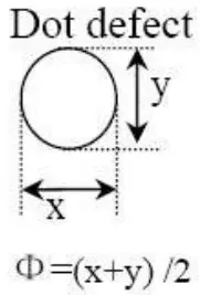 | Zone Size(mm) | Acceptable Qty | Minor | |||||||||||||||||||||||||||||||||||||||
| A+B | C | ||||||||||||||||||||||||||||||||||||||||||
| 3.5”~7” | 7~10.1” | >10.1” | |||||||||||||||||||||||||||||||||||||||||
| Φ≤0.2 | Acceptable | Acceptable | Acceptable | Acceptable | |||||||||||||||||||||||||||||||||||||||
| 0.2<Φ≤0.5 | 4 | 5 | 6 | ||||||||||||||||||||||||||||||||||||||||
| Φ>0.5 | 0 | 0 | 0 | ||||||||||||||||||||||||||||||||||||||||
| Note: 1. Minimum distance between defective dots is more than 5 mm; 2. The quantity of defect is zero in operating condition. | |||||||||||||||||||||||||||||||||||||||||||
| 3 | Linear defect |
| Minor | ||||||||||||||||||||||||||||||||||||||||
| 4 | Polarizer defect | 5.4.1 Polarizer Position ( i) Shifting in position should not exceed the glass outline dimension. ( ii ) Incomplete covering of the viewing area due to shifting is not allowed. 5.4.2 Dirt on polarizer Dirt which can be wiped easily should be acceptable. 5.4.3 Polarizer Dent & Air bubble 5.4.4 Polarizer scratch (i) If the polarizer scratch can be seen after cover assembling or in the operating condition, judge by the linear defect of 5.3. ( ii )If the polarizer scratch can be seen only in non-operating condition or some special angle, judge by the following: | Minor | |||||||
| Zone Size (mm) | Acceptable Qty | |||||||||
| A+B |
C | |||||||||
| Length | Width | 3.5”~7” | 7~10.1” | >10.1” | ||||||
| Ignore | W≤0.05 | Acceptable | Acceptable | Acceptable | Acceptable | |||||
| 1.0<L ≤5.0 | 0.05< W≤0.20 | 4 | 5 | 6 | ||||||
| L>5.0 | W>0.2 | 0 | 0 | 0 | ||||||
| 5 | MURA | Using 3% ND filter, it’s NG if it can be seen in R,G,B picture. | Minor | |||||||
| White/Black dot(MURA) | Visible under:ND3%;D≦0.15mm, Acceptable; 0.15mm<D≦0.5mm, N≦4;D>0.5mm, Not allowable. | |||||||||
| 6 | Glass defect | (i) Crack Cracks are not allowed.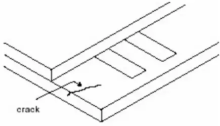 | Minor | ||||||
(ii) TFT chips on corner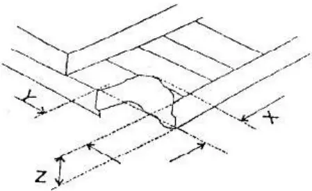
Chips on the corner of terminal shall not be allowed to extend into the ITO pad or expose perimeter seal. | Minor | ||||||||
(iii) Usual surface crack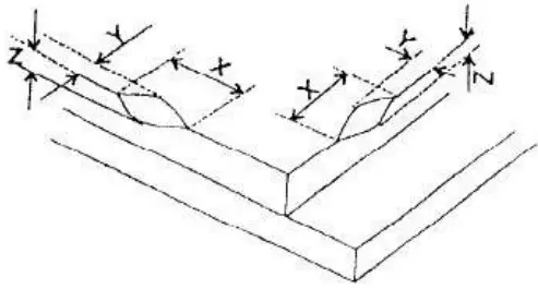
It is only applicable to the upper glass of LCD. | Minor |
| Item No. | Items to be inspected | Inspection Standard | Classification of defects |
| 1 | Difference in Spec. | Not allowable | Major |
| 2 | Pattern peeling | No substrate pattern peeling and floating | Major |
| 3 | Soldering defects | No soldering missing | Major |
| No soldering bridge | Major | ||
| No cold soldering | Minor | ||
| 4 | Resist flaw on PCB | Visible copper foil (Φ0.5 mm or more) on substrate pattern is not allowed | Minor |
| 5 | FPC gold finger | No dirt, breaking, oxidation lead to black | Major |
| 6 | Backlight plastic frame | No deformation, crack, breaking, backlight positioning column breaking, obvious nick. | Minor |
| 7 | Marking printing effect | No dark marking, incomplete, deformation lead to unable to judge | Minor |
| 8 | Accretion of metallic Foreign matter | No accretion of metallic foreign matter (Not exceed Φ0.2mm) | Minor |
| 9 | Stain | No stain to spoil cosmetic badly | Minor |
| 10 | Plate discoloring | No plate fading, rusting and discoloring | Minor |
| 11 | 1. Lead parts | a. Soldering side of PCB Solder to form a ‘Filet’ all around the lead. Solder should not hide the lead form perfectly. | Minor |
| b. Components side(In case of ‘Through Hole PCB’) Solder to reach the Components side of PCB. | Minor | ||
| 2. Flat packages | Either ‘Toe’(A) or ‘Seal’(B)of the lead to be covered by “Filet”. Lead form to be assume over Solder.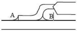 | Minor | |
| 3. Chips | (3/2) H ≥h ≥(1/2) H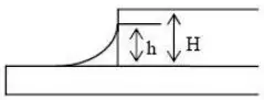 | Minor | |
| 4. Solder ball/Solder splash | a. The spacing between solder ball and the conductor or solder pad h ≥0.13 mm. The diameter of solder ball d≤0.15 mm. | Minor | |
| b. The quantity of solder balls or solder splashes isn’t beyond 5 in 600 mm2. | Minor | ||
| c. Solder balls/Solder splashes do not violate minimum electrical clearance. | Major |


Shenzhen Sorento Technology Co.,Ltd.
www.surenoo.com
Skype: Surenoo365
Reference Controller Datasheet
MCU Interface LCD Module Selection Guide
LT7381


