infineon TRAVEO T2G Bootloader
TRAVEO™ T2G bootloader
About this document
Scope and purpose
This application note describes a CAN/LIN-based bootloader for TRAVEO™ T2G Family. This application note also explains how to communicate with a CAN/LIN-based bootloader.
Intended audience
This document is intended for anyone using TRAVEO™ T2G bootloader.
Associated Part Family
TRAVEO™ T2G family
Introduction
Bootloaders are commonly present in an MCU system design. A bootloader makes it possible for a product’s firmware to be updated in the field. At the factory, the firmware is initially programmed into a product typically through the MCU’s Joint Test Action Group (JTAG) interface or the Arm® serial wire debug (SWD) interface. However, these interfaces are usually not accessible in the field.
Bootloading is a process that allows you to upgrade your system firmware over an automotive standard communication interface such as CAN or LIN. A bootloader communicates with a host to get new application code or data and writes it into the device’s flash memory.
In this application note, you will learn how to communicate with a CAN/LIN-based bootloader.
This application note assumes that you are familiar with bootloader concepts, and CAN and LIN protocols. For more details on CAN and LIN Components, see the “Flash Boot”, “CAN FD Controller”, and “Local Interconnect Network” chapters of the architecture technical reference manual.
Terms and definitions
Figure 1 illustrates the main elements in a bootloader system. It shows that the product’s embedded firmware must be able to use the communication port for two different purposes: normal operation and updating the flash. The portion of the embedded firmware that knows how to update the flash is called the “bootloader.” The other terms in Figure 1 are defined in the following paragraphs.
 Figure 1 Bootloading system diagram
The system that provides the data to update the flash is called the “host”, and the system being updated is called the “target”. The host can be an external PC (a PC host) or another MCU.
The act of transferring data from the host to the target is called “bootloading”, or a “bootload” operation, or a “bootload” for short. The firmware that is placed in the memory is called the “application” or the “bootloadable”.
Using a bootloader
A bootloader communication port is typically shared between the bootloader and the actual application. The first step in using a bootloader is to manipulate the target so that the bootloader and not the application is executed.
Once the bootloader is running, the host can send an Enter Bootloader command over the communication channel. If the bootloader sends an OK response, bootloading can begin.
Bootloader function flow
During bootloading, the host reads the file for the new application, parses it with the commands downloaded to the RAM, and sends those commands to the bootloader. After the entire file is sent, the bootloader can pass control to the new application.
An internal bootloader typically executes in flash boot after the device resets.
The bootloader can then perform the following actions:
- Check the new application’s validity before transferring control to that application
- Manage the timing to start host communication
- Perform the bootloading operation
- Pass control to the new application
Figure 2 shows the bootloading sequence.
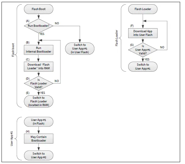 Figure 2 Bootloading sequence
- (A) The flash boot checks whether the internal bootloader (part of the flash boot) should be run.
- (B) The Internal bootloader is a part of the flash boot firmware that has the goal of downloading the flash loader into the RAM
- (C) and launching it (E).
- (D) The flash loader requires neither a secure signature nor an encryption. However, the checksum (CRC-32C) must be placed in the last 4 bytes of the flash loader if the host uses the Verify Application command.
- (F) The flash loader downloads a user application through CAN or LIN communication and stores it in the code flash or work flash.
- (G) The flash loader verifies the user application for integrity. If the user application signature verification fails, the flash loader tries to restart bootloading and receive a new image.
- (H) The user application may or may not contain a bootloader. It is up to the user.
Note that only the flash boot part of the bootloading sequence (A) to (E) is developed as the flash boot firmware; the remaining sequence is developed by the user.
Device interface configuration
The bootloader enables end-of-line programming using only CAN or LIN when the following conditions are met:
- Two words at the start of the flash must be ‘0xFFFFFFFF’.
- TOC2 is valid and internal bootloader is enabled (default) by TOC2_FLAGS.FB_BOOTLOADER_CTL bits, or TOC2 is empty
- Protection mode is not SECURE and not SECURE_DEAD.
- No debugger connection happened during the one-second wait window.
First, the bootloader prepares the channel configuration for CAN and waits for the preconfigured time for the frame from the host. If there is a timeout, the channel is reconfigured for LIN and it again waits for the frame. If no frame from the host is received, this procedure is repeated for 300 seconds, which is the overall bootloading time as shown in Figure 3.
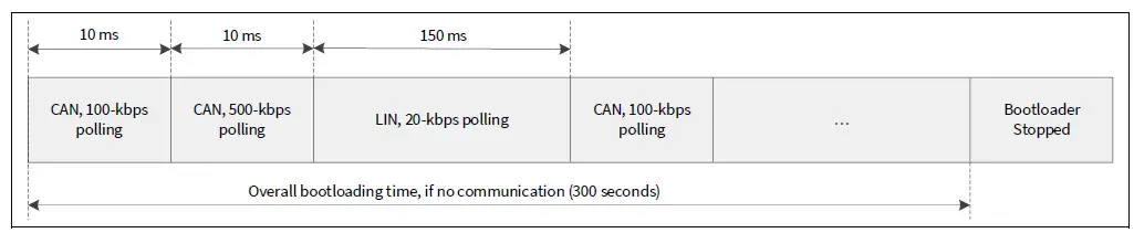 Figure 3 Bootloader polling sequence
If an Enter Bootloader command is received on either of the communication interfaces, the polling stops and the bootloader starts using this interface only. If the bootloading succeeds, the bootloader launches the updated application in the RAM. This application is called a “flash loader”.
Figure 4 shows the default startup timing on a new device without firmware in the flash. Note that once the firmware is written to the flash, the internal bootloader is no longer launched. See the device-specific datasheet for the defined time.
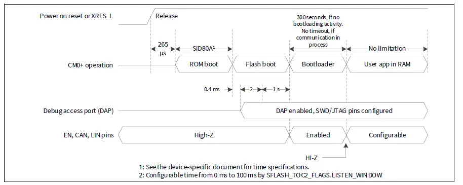 Figure 4 Startup timing
CAN configuration
Table 1 shows the CAN configuration. Figure 5 shows the CAN interface configuration. The flash boot sets two EN pins and the TX pin as strong drive mode on entering the bootloader. The RX pin is in the High-Z mode. Before or after the bootloader, these pins are configured in the High-Z mode. The EN pins can be used to enable the CAN transceiver. If you keep the CAN transceiver always enabled, you do not need to use the EN pins.
Table 1 CAN configuration
| Parameter | Configuration | |||
| CYT2B, CYT3B, CYT4B | CYT2C | CYT3D | CYT4D, CYT4E | |
| CAN instance | CAN0_1 | CAN0_0 | CAN0_0 | CAN1_0 |
| TX pin | P0.2/CAN0_1_TX | P18.2/CAN0_0_TX | P5.4/CAN0_0_TX | P2.3/CAN1_0_TX |
| RX pin | P0.3/CAN0_1_RX | P18.3/CAN0_0_RX | P5.5/CAN0_0_RX | P2.4/CAN1_0_RX |
| EN (HIGH) pin | P2.1 (optional) | P19.2 (optional) | P2.1 (optional) | P0.2 (optional) |
| EN (LOW) pin | P23.3 (optional) | P19.3 (optional) | P2.0 (optional) | P0.5 (optional) |
| CAN mode | CAN classic mode (CAN FD mode is not in use) | |||
| Baud rate | 100 kbps or 500 kbps | |||
| RX message ID | 0x1A1 | |||
| TX message ID | 0x1B1 | |||
| Phase segment 1 | 39 tq (time quantum) | |||
| Phase segment 2 | 10 tq (time quantum) | |||
| SJW (Resynchronization jump width) | 10 tq (time quantum) | |||
| Sampling point | 80 % | |||
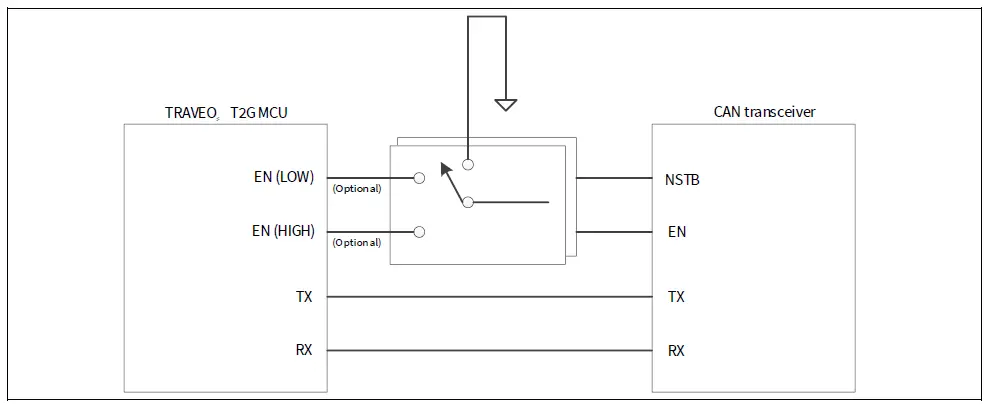 Figure 5 CAN interface configuration
| Parameter | Configuration | |||
| CYT2B, CYT3B, CYT4B | CYT2C | CYT3D | CYT4D, CYT4E | |
| LIN instance | LIN1 | LIN0 | LIN0 | LIN1 |
| TX pin | P0.1/LIN1_TX | P19.0/LIN0_0_TX | P1.6/LIN0_TX | P0.0/LIN1_TX |
| RX pin | P0.0/LIN1_RX | P19.1/LIN0_0_RX | P1.7/LIN0_RX | P0.1/LIN1_RX |
| EN (HIGH) pin | P2.1 (optional) | P19.2 (optional) | P2.1 (optional) | P0.2 (optional) |
| EN (LOW) pin | P23.3 (optional) | P19.3 (optional) | P2.0 (optional) | P0.5 (optional) |
| LIN mode | Slave | |||
| Baud rate | 20 kbps or 115.2 kbps (as an option for fast flash programming) | |||
| Break field length | 11 bits | |||
| Break delimiter length | 1 bit | |||
| Stop bit | 1 bit | |||
| PID (RX) | 45 | |||
| PID (TX) | 46 | |||
| Checksum type | Classic | |||
LIN configuration
Table 2 shows the LIN configuration. Figure 6 shows the LIN interface configuration. Note that all LIN transceivers do not support 115.2 kbps (Fast mode). The flash boot sets two EN pins and the TX pin in strong drive mode on entering the bootloader. The RX pin is in the High-Z mode for all devices except CYT3D. For this device, the RX pin is set in resistive pull-up drive mode. Before or after the bootloader, these pins are configured in the High-Z mode.
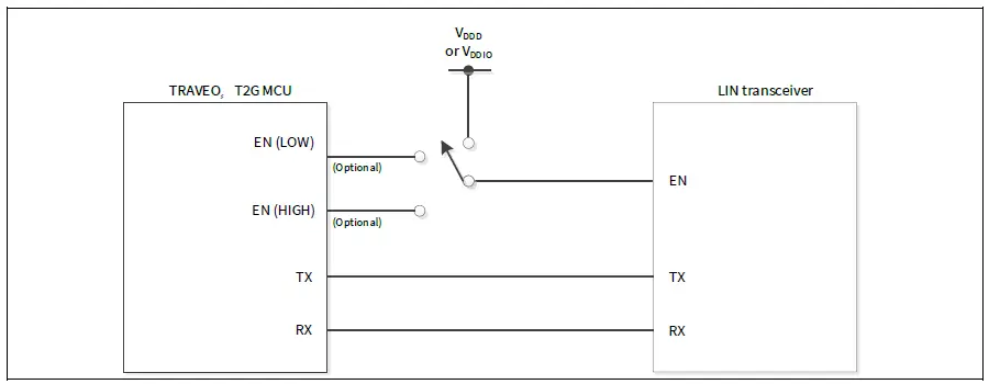 Figure 6 LIN interface configuration
LIN configuration for 115.2 kbps
Some LIN transceivers require the special signals on TX and EN pins, as shown in Figure 7, to enter a Fast mode which supports 115.2 kbps. Some LIN transceivers support 115.2 kbps without the special signals.
 Figure 7 Signal timing for fast mode
First, the bootloader waits for an Enter Bootloader command on LIN at 20 kbps. When the Enter Bootloader command is received, the bootloader expects the next command to be Set Application Metadata. If Set
Application Metadata has an Application ID = ‘0’, the bootloader continues at 20 kbps. If Set Application Metadata has an Application ID = ‘1’, the bootloader switches to 115.2 kbps using the special signals. If Set Application Metadata has Application ID = ‘2’, the bootloader switches to 115.2 kbps without the special signals.
Communication flow
Figure 8 shows the example of a communication flow between the host and bootloader. Figure 8 gives the order in which commands are issued to the target and responses are received. See Command/response packet structure and Commands for a complete list of bootloader commands, their codes, and their expected responses.
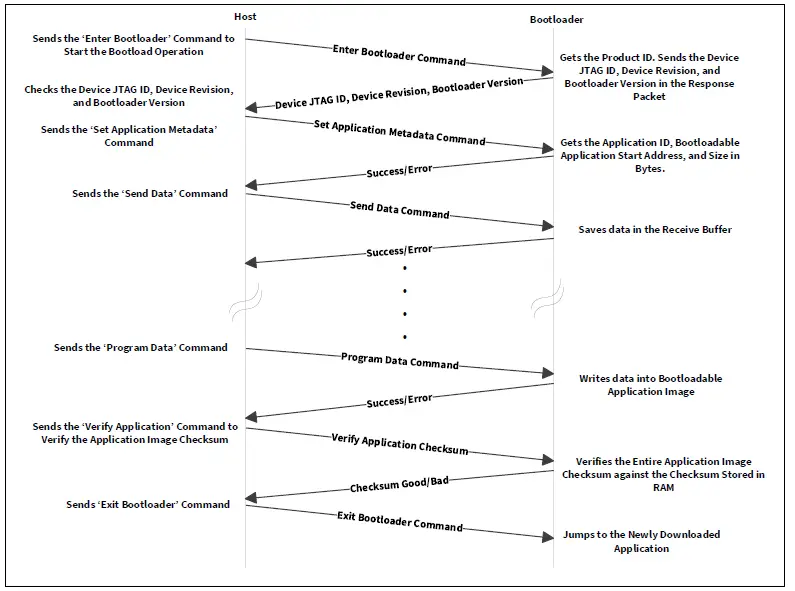 Figure 8 Communication flow
Command/response packet structure
The commands and responses are in the form of a byte stream, packetized in a manner that ensures the integrity of the data being transmitted. Each packet includes checksum bytes. The checksum is a basic summation (2’s complement).
When sending multibyte data such as Data Length and Checksum, the least significant byte is sent first. The bootloader packet length is limited to four CAN or LIN messages, each with 8 bytes of data. Each CAN or LIN message can contain up to 8 bytes of user data, which holds bootloader command data. The message length must be adjusted to the actual packet size.
Figure 9 shows the structure of the communication packets sent from the host to the bootloader.
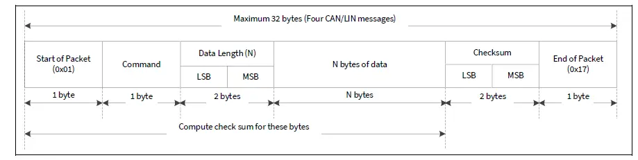 Figure 9 Command packet structure
Figure 10 shows the structure of the response packets sent from the bootloader to the host.
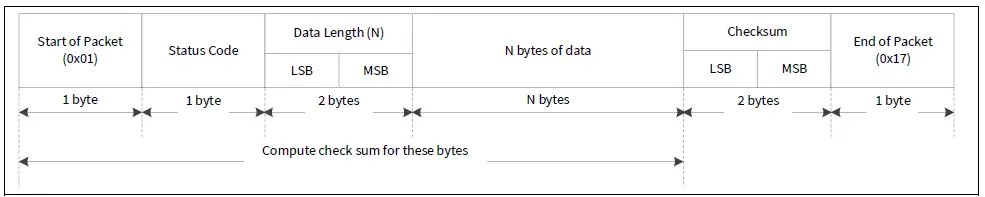 Figure 10 Response packet structure
The bootloader responds to each command from the host with a response packet. The format of the response packet is similar to the command packet except that there will be a status code instead of the command code.
Commands
Table 3 shows a list of commands supported by the bootloader. All commands except ‘Exit Bootloader’ are ignored until the ‘Enter Bootloader’ command is received.
Table 3 Commands list
Commands
| Enter/Exit | Bootload operation | Miscellaneous |
| Enter Bootloader | Send Data | Verify Application |
| Sync Bootloader | Send Data Without Response | Set Application Metadata |
| Exit Bootloader | Program Data |
There is no specific requirement for command execution time.
Table 4 shows a list of status codes supported by the bootloader.
Table 4 Status codes list
| Status code | Value | Description |
| CY_BOOTLOAD_SUCCESS | 0x00 | Bootload operation successful |
| CY_BOOTLOAD_ERROR_VERIFY | 0x02 | Error verifying the application image |
| CY_BOOTLOAD_ERROR_LENGTH | 0x03 | Unexpected or incorrect data length |
| CY_BOOTLOAD_ERROR_DATA | 0x04 | Data in bootloader command packet is incorrect |
| CY_BOOTLOAD_ERROR_CMD | 0x05 | Command byte is not recognized |
| CY_BOOTLOAD_ERROR_CHECKSUM | 0x08 | Bootloader packet has incorrect checksum |
| CY_BOOTLOAD_ERROR_ROW | 0x0A | Incorrect address to bootload an application |
| CY_BOOTLOAD_ERROR_ROW_ACCESS | 0x0B | Address cannot be accessed due to MPU or SWPU protection |
| CY_BOOTLOAD_UNKNOWN | 0x0F | Any other error condition |
Enter Bootloader
This command begins a bootloading operation. All other commands except ‘Exit Bootloader’ are ignored until this command is received. This command responds with the device information and bootloader version.
Input
- Command Byte: 0x38
- Data Bytes:
- 4 bytes: Product ID. Must be 0x01020304.
Output
- Status Codes:
- Success
- Error Command
- Error Data used for product ID mismatch
- Error Length
- Error Checksum
- Data Bytes:
- 4 bytes: Device JTAG ID
- 1 byte: Device revision
- 3 bytes: Bootloader version
Sync Bootloader
This command resets the bootloader communication to the initial state, making it ready to accept a new command. Any data that was buffered is discarded. This command is needed only if the bootloader and the host get out of sync with each other.
Input
- Command Byte: 0x35
- Data Bytes: N/A
Output
- N/A
- This command is not acknowledged
Exit Bootloader
This command stops listening for other bootloader commands and jumps to the newly downloaded application (flash loader).
Input
- Command Byte: 0x3B
- Data Bytes: N/A
Output
- N/A – This command is not acknowledged
Send Data
This command transfers a block of data to the bootloader. This data is buffered in anticipation of a Program Data command. The bootloader buffer size for the data received by Send Data and Program Data commands is 256 bytes. If the data is not programmed using Program Data and the data is still sent, the buffer will overflow and the CY_BOOTLOAD_ERROR_LENGTH error will be sent in the response packet. If a sequence of multiple send data commands is sent, the data is appended to the previous block.
This command is used to break up large data transfers into smaller pieces to prevent channel starvation in some communication protocols. If the host uses the Verify Application command, the checksum (CRC-32C) for the entire application must be placed in the last four bytes of the application image.
Input
- Command Byte: 0x37
- Data Bytes:
- n bytes: Data to write
Output
- Status Codes:
- Success
- Error Command
- Error Data
- Error Length
- Error Checksum
- Data Bytes: N/A
Send Data without Response
This command is same as the Send Data command, except that no response is generated by the bootloader. This reduces bootloading time for some applications.
Input
- Command Byte: 0x47
- Data Bytes:
- n bytes: Data to write
Output
- N/A
Program Data
This command writes data into the bootloadable application image, and might follow a series of Send Data or Send Data Without Response commands.
Input
- Command Byte: 0x49
- Data Bytes:
- 4 bytes: Address. Must be aligned to 256 bytes and within a valid RAM memory length – [RAM_START + 3 KB, RAM_END – 6 KB].
- 4 bytes: CRC-32C of the entire n bytes of the data in the buffer which has been previous transferred using the Send Data command.
- n bytes: An arbitrary value.
Output
- Status Codes:
- Success
- Error Command
- Error Data
- Error Length
- Error Checksum
- Error Row
- Error Row Access
- Data Bytes: N/A
Verify Application
This command reports whether the checksum (CRC-32C) for the entire application image (flash loader) in the RAM is valid. The host can decide to use the Verify Application command or to skip it. The checksum (CRC-32C) for the entire application must be placed in the last four bytes of the application image.
Input
- Command Byte: 0x31
- Data Bytes:
- 1 byte: Application ID of the application to be verified. Must be the same value as in the Set Application Metadata command.
Output
- Status Codes:
- Success
- Error Command
- Error Data
- Error Length
- Error Checksum
- Error Row Access
- Data Bytes:
- 1 byte: 0x01 indicates that application is valid. 0x00 indicates that application is invalid.
Set Application Metadata
This command is used to set a given application’s metadata. This command must be the second bootloader command which the host delivers to the MCU, the first one being Enter Bootloader.
Input
- Command Byte: 0x4C
- Data Bytes:
- 1 byte: Application ID
Table 5 shows the values of application ID.
Table 5 Application ID
| Application ID value | Description |
| 0 | For either LIN at 20 kbps or CAN |
| 1 | For LIN at 115.2 kbps with a Fast mode. See LIN configuration for 115.2 kbps. |
| 2 | For LIN at 115.2 kbps without a Fast mode. |
- 4 bytes: Bootloadable application start address. Must be aligned to 256 bytes and within a valid RAM memory length – [RAM_START + 3 KB, RAM_END – 6 KB].
- 4 bytes: Bootloadable application size in bytes. Must be a value for which the bootloadable application image fits into a RAM address range [RAM_START + 3 KB, RAM_END – 6 KB].
Output
- Status Codes:
- Success
- Error Command
- Error Length
- Error Data
- Error Checksum
- Error Row Access
- Data Bytes: N/A
Application format
Figure 11 shows an example of an application format. If the host uses the Verify Application command, the checksum (CRC-32C) for the entire application must be placed in the last four bytes of the application image.

Figure 11 Example for application format
Example command/response data
Table 6 shows the example data for each command/response. If a sequence of multiple Send Data commands is sent, the data is appended to the previous block. This command is used to break up large data transfers into smaller pieces to prevent channel starvation in some communication protocols.
Table 6 Example command/response data
| Command/ response | Start of packet | Command/ status code | Data length | N bytes of data | Checksum | End of packet |
| Enter Bootloader | 0x01 | 0x38 | 0x04, 0x00 | 0x04, 0x03, 0x02, 0x01 | 0xB9, 0xFF | 0x17 |
| Response | 0x01 | 0x00 | 0x08, 0x00 | 0x00, 0x00, 0x00, 0x00, 0x00, 0x14, 0x02, 0x01 | 0xE0, 0xFF | 0x17 |
| Set Application Metadata | 0x01 | 0x4C | 0x09, 0x00 | 0x00, 0x00, 0x40, 0x00, 0x08, 0xFC, 0x7F, 0x00, 0x00 | 0xE7, 0xFD | 0x17 |
| Response | 0x01 | 0x00 | 0x00, 0x00 | – | 0xFF, 0xFF | 0x17 |
| Send Data | 0x01 | 0x37 | 0x19, 0x00 | 0x00, 0xE0, 0x00, 0x08, 0xF1, 0x49, 0x00, 0x08, 0x7F, 0x49, 0x00, 0x08, 0xF9, 0x4A, 0x00, 0x08, 0x00, 0x00, 0x00, 0x00, 0x00, 0x00, 0x00, 0x00, 0x00 | 0x6A, 0xFB | 0x17 |
| Response | 0x01 | 0x00 | 0x00, 0x00 | – | 0xFF, 0xFF | 0x17 |
| Program Data | 0x01 | 0x49 | 0xE0, 0x00 | 0x00, 0x40, 0x00, 0x08, 0x91, 0xE6, 0x0D, 0xD8, 0xFF, 0xFF, 0xFF 0xFF, 0xFF, 0xFF | 0x0A, 0xF7 | 0x17 |
| Response | 0x01 | 0x00 | 0x00, 0x00 | – | 0xFF, 0xFF | 0x17 |
| Verify Application | 0x01 | 0x31 | 0x01, 0x00 | 0x00 | 0xCD, 0xFF | 0x17 |
| Response | 0x01 | 0x00 | 0x01, 0x00 | 0x01 | 0xFD, 0xFF | 0x17 |
| Exit Bootloader | 0x01 | 0x3B | 0x00, 0x00 | – | 0xC4, 0xFF | 0x17 |
Glossary
Table 7 Glossary
| Terms | Description |
| CAN FD | Controller Area Network with Flexible Data rate |
| CRC | Cyclic Redundancy Check |
| DAP | Debug Access Port |
| JTAG | Joint Test Action Group |
| LIN | Local Interconnect Network |
| MPU | Memory Protection Unit |
| SJW | Resynchronization Jump Width |
| SWD | Single Wire Debug |
| TOC2 | Table of Contents 2 |
| tq | Time Quantum |
The following are the TRAVEO™ T2G family series datasheets and technical reference manuals. Contact Technical support to obtain these documents.
- Device datasheet
- CYT2B7 datasheet 32-bit Arm® Cortex®-M4F microcontroller TRAVEO™ T2G family
- CYT2B9 datasheet 32-bit Arm® Cortex®-M4F microcontroller TRAVEO™ T2G family
- CYT4BF datasheet 32-bit Arm® Cortex®-M7 microcontroller TRAVEO™ T2G family
- CYT4DN datasheet 32-bit Arm® Cortex®-M7 microcontroller TRAVEO™ T2G family (Doc No. 002-24601)
- CYT3BB/4BB datasheet 32-bit Arm® Cortex®-M7 microcontroller TRAVEO™ T2G family
- CYT3DL datasheet 32-bit Arm® Cortex®-M7 microcontroller TRAVEO™ T2G family (Doc No. 002-27763)
- CYT4EN datasheet 32-bit Arm® Cortex®-M7 microcontroller TRAVEO™ T2G family (Doc No. 002-30842)
- CYT2CL datasheet 32-bit Arm® Cortex®-M4F microcontroller TRAVEO™ T2G family (Doc No. 002- 32508)
- Technical reference manual
- Body controller entry family
- TRAVEO™ T2G automotive body controller entry family architecture technical reference manual (TRM)
- TRAVEO™ T2G automotive body controller entry registers technical reference manual (TRM) for CYT2B7
- TRAVEO™ T2G automotive body controller entry registers technical reference manual (TRM) for CYT2B9
- Body controller high family
- TRAVEO™ T2G automotive body controller high family architecture technical reference manual (TRM)
- TRAVEO™ T2G automotive body controller high registers technical reference manual (TRM) for CYT4BF
- TRAVEO™ T2G automotive body controller high registers technical reference manual (TRM) for CYT3BB/4BB
- Cluster 2D family
- TRAVEO™ T2G automotive cluster 2D family architecture technical reference manual (TRM) (Doc No. 002-25800)
- TRAVEO™ T2G automotive cluster 2D registers technical reference manual (TRM) for CYT4DN (Doc No. 002- 25923)
- TRAVEO™ T2G automotive cluster 2D registers technical reference manual (TRM) for CYT3DL (Doc No. 002- 29854)
- TRAVEO™ T2G automotive cluster 2D registers technical reference manual (TRM) for CYT4EN (Doc No. 002- 32087)
- Cluster entry family
- TRAVEO™ T2G automotive cluster entry family architecture technical reference manual (TRM) (Doc No. 002- 33175)
- TRAVEO™ T2G automotive cluster entry registers technical reference manual (TRM) (Doc No. 002-33404)
Revision history
| Document version | Date of release | Description of changes |
| ** | 2019-08-23 | New application note. |
| *A | 2021-02-24 | Updated Introduction: Updated Device interface configuration: Updated description. Updated Figure 4. Updated CAN configuration: Updated description. Updated Table 1. Updated Figure 5. Updated LIN configuration: Updated description. Updated Table 2. Updated Figure 6. Updated Commands: Updated Program Data: Updated description. Updated Set Application Metadata: Updated description. Updated Example command/response data: Updated Table 6. Updated Related Documents: Updated description. Updated to Infineon template. |
| *B | 2021-06-14 | Added “Associated Part Family” in page 1. |
| *C | 2022-10-19 | Updated Figure 4, Table 1, Table 2. Updated Related documents. |
Trademarks
All referenced product or service names and trademarks are the property of their respective owners.
Edition 2022-10-19
Published by
Infineon Technologies AG
81726 Munich, Germany
© 2022 Infineon Technologies AG. All Rights Reserved.
Do you have a question about this document?
Go to www.infineon.com/support
Document reference
002-27076 Rev. *C
IMPORTANT NOTICE
The information contained in this application note is given as a hint for the implementation of the product only and shall in no event be regarded as a description or warranty of a certain functionality, condition or quality of the product. Before implementation of the product, the recipient of this application note must verify any function and other technical information given herein in the real application. Infineon Technologies hereby disclaims any and all warranties and liabilities of any kind (including without limitation warranties of non-infringement of intellectual property rights of any third party) with respect to any and all information given in this application note.
The data contained in this document is exclusively intended for technically trained staff. It is the responsibility of customer’s technical departments to evaluate the suitability of the product for the intended application and the completeness of the product information given in this document with respect to such application.
For further information on the product, technology, delivery terms and conditions and prices please contact your nearest Infineon Technologies office (www.infineon.com).
WARNINGS
Due to technical requirements products may contain dangerous substances. For information on the types in question please contact your nearest Infineon Technologies office.
Except as otherwise explicitly approved by Infineon Technologies in a written document signed by authorized representatives of Infineon
Technologies, Infineon Technologies’ products may not be used in any applications where a failure of the product or any consequences of the use thereof can reasonably be expected to result in personal injury.
References
 Semiconductor & System Solutions - Infineon Technologies
-
Support: Live Chat Online, Tech Support & FAQ - Infineon Technologies
-
cypress.com/documentation/datasheets/cyt2b7-datasheet-32-bit-arm-cortex-m4f-microcontroller-traveo-ii-family
-
cypress.com/documentation/datasheets/cyt2b9-datasheet-32-bit-arm-cortex-m4f-microcontroller-traveo-ii-family
-
cypress.com/documentation/datasheets/cyt3bb4bb-datasheet-32-bit-arm-cortex-m7-microcontroller-traveo-ii-family
-
cypress.com/documentation/datasheets/cyt4bf-datasheet-32-bit-arm-cortex-m7-microcontroller-traveo-ii-family
-
cypress.com/documentation/technical-reference-manuals/traveo-ii-automotive-body-controller-entry-family
-
cypress.com/documentation/technical-reference-manuals/traveo-ii-automotive-body-controller-entry-registers-trm
-
cypress.com/documentation/technical-reference-manuals/traveo-ii-automotive-body-controller-high-family
-
cypress.com/documentation/technical-reference-manuals/traveo-tm-ii-automotive-body-controller-high-registers
-
cypress.com/documentation/technical-reference-manuals/traveotm-ii-automotive-body-controller-high-registers
-
Semiconductor & System Solutions - Infineon Technologies
-
Support: Live Chat Online, Tech Support & FAQ - Infineon Technologies


