![]() WS4611
WS4611
80mΩ, Current Limited, Power Distribution Switch
www.ovt.com
Descriptions
The WS4611 is a high-side switch with ultra-low ON resistance P-MOSFET. The integrated current-limit function can limit inrush current for heave capacitive load, over load current, and short-circuit current to protect the power source. 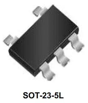
The WS4611 is also an integrated reverse protection function to eliminate any reverse current flow across the switch when the device is off. The thermal shutdown function can protect the device and load. The output auto-discharge function is disabled in WS4611. The WS4611 is available in the SOT-23-5L package. The standard product is Pb-free and Halogen-free.
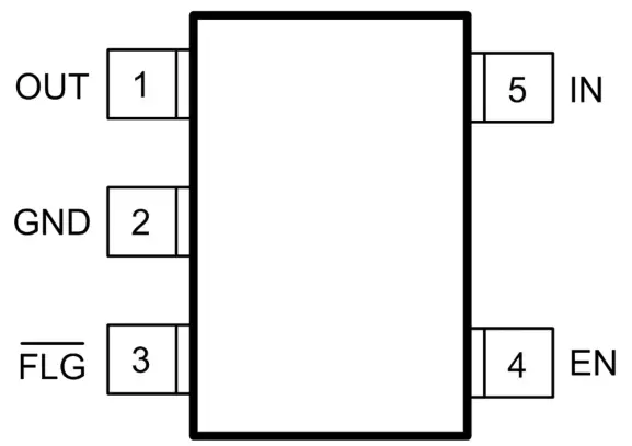 Pin configuration (Top view)
Features
- Input voltage range : 2.5~5.5V
- Main switch RON : 80mΩ @ VIN=5V
- Current limit threshold – WS4611EB: 1.0A (Typ.)
- Reverse block (No “body diode”)
- Over temperature protection
Applications
- USB peripherals
- USB Dongle
- USB 3G data card
- 3.3V or 5V Power Switch
- 3.3V or 5V Power Distribution
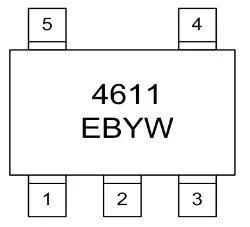
4611 = Device code
EB = Special code
Y = Year code
W = Week code
Marking
Order information
| Device | Package | Shipping |
| WS4611EB-5/TR | SOT-23-5L | 3000/Reel&Tape |
Typical Applications
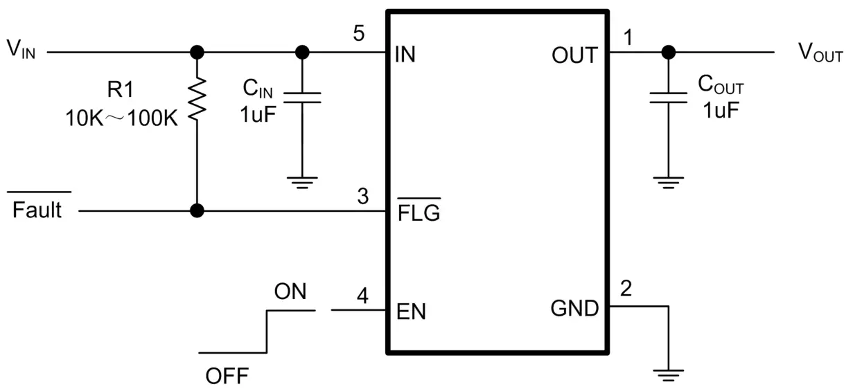
Pin Descriptions
| Pin Number | Symbol | Descriptions |
| 1 | OUT | Output Pin |
| 2 | GND | Ground |
| 3 | FLG | Fault Flag Pin, Open-Drain, Active Low |
| 4 | EN | Enable Pin, Active High |
| 5 | IN | Input Pin |
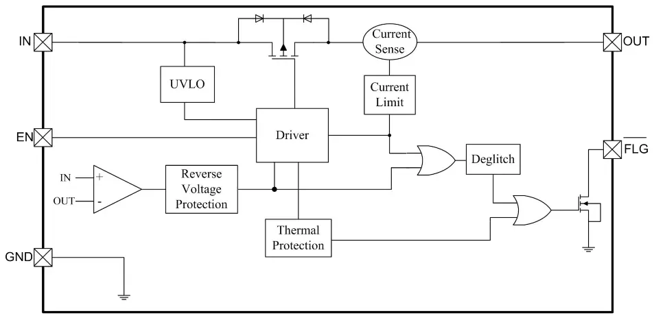
Block Diagram
Absolute maximum ratings
| Parameter | Symbol | Value | Unit |
| IN pin voltage range | VIN | -0.3~6.5 | V |
| OUT pin voltage range | VOUT | -0.3~6.5 | V |
| FLG pin voltage range | VFLG | -0.3~6.5 | V |
| EN pin voltage range | VEN | -0.3~6.5 | V |
| Junction temperature | TJ | -40~150 | oC |
| Lead temperature(Soldering, 10s) | TL | 260 | oC |
| Storage temperature | Tstg | -55 ~ 150 | oC |
| IN, OUT Pin ESD Ratings | HBM | 8000 | V |
| MM | 400 | V | |
| FLG, EN Pin ESD Ratings | HBM | 4000 | V |
| MM | 400 | V |
These are stress ratings only. Stresses exceeding the range specified under “Absolute Maximum Ratings” may cause substantial damage to the device. Functional operation of this device at other conditions beyond those listed in the specification is not implied and prolonged exposure to extreme conditions may affect device reliability.
Recommend Operating Conditions
| Parameter | Symbol | Value | Unit |
| Supply input voltage range | VIN | 2.5~5.5 | V |
| Operating ambient temperature | TA | -40~85 | oC |
| Thermal Resistance | RθJA | 250 | oC/W |
Electronics Characteristics (Ta=25o C, VIN=5V, CIN=COUT=1μF, unless otherwise noted)
| Parameter | Symbol | Conditions | Min. | Typ. | Max. | Units |
| Quiescent supply current | IQ | IOUT=0, VIN=VEN=5V | 48 | 60 | μA | |
| Shutdown current | ISD | VEN=0V | 1 | μA | ||
| Reverse current | IREV | VIN=VEN=0V, VOUT=5V, Current flow to VIN | 1 | μA | ||
| Main-FET ON resistance(1) | RON | VIN=VEN=5V, IOUT=500mA | 80 | mΩ | ||
| Auto-discharge FET ON resistance | RDCHG | VEN=0V, VIN =VOUT=5V | 65 | Ω | ||
| Over-current trip threshold | IOC | Current ramp (≤100A/s) on OUT | 0.7 | 1 | 1.4 | A |
| Short-circuit output current | IOS | OUT shorted to GND | 0.45 | A | ||
| Short circuit current limiting response time | tSHORT | OUT connected to GND,CL=1μF | 2 | μs | ||
| EN input low voltage | VIL | VIN=5V | 0.4 | V | ||
| EN input high voltage | VIH | VIN=5V | 1.6 | V | ||
| OUT pin turn-on time after EN ON | tON | CL=1μF, RL=5ohm | 20 | μs | ||
| Fault flag output blanking time | blank | 9 | ms | |||
| Over-temperature shutdown threshold | TSD | 160 | oC | |||
| Over-temperature threshold hysteresis | THYS | 35 | oC | |||
| Under voltage lock-out threshold | VOLVO | 2.2 | V | |||
| Under voltage lockout hysteresis | VOLVO-HYS | 200 | mV |
Note: (1) Pulse test, TP=380us
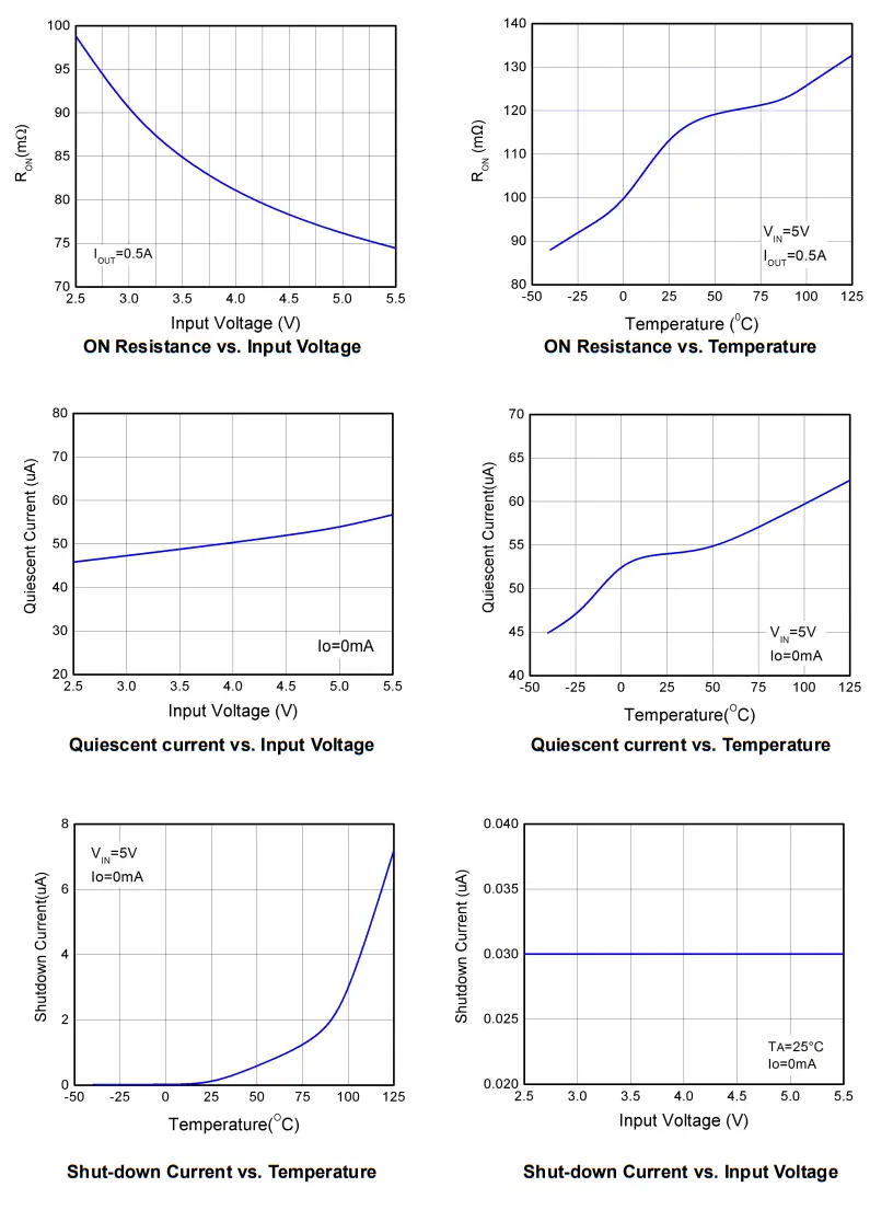
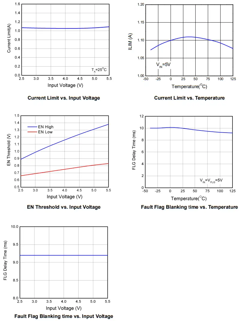
Typical Characteristics (Ta=25 o C, unless otherwise noted)
 |  | Startup from Power ON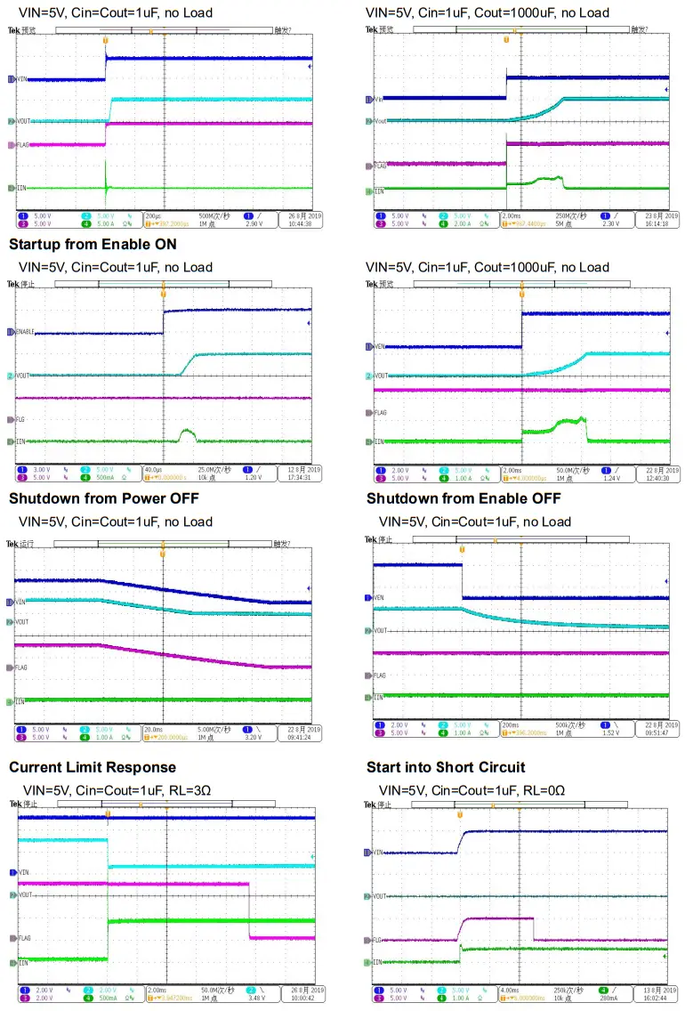 |
Operation Information
Power Switch
The power switch is a P-channel MOSFET with low RDS(ON) for power management or USB power distribution applications. The WS4611 has reverse voltage protection to prevent current flow from OUT to IN and IN to OUT when the device is off.
Current-Limit Protection
The WS4611 provides a current limit protection function to protect the power source when the over-current condition occurs.
Short-Circuit Protection
The WS4611 provides a short circuit protection function. The output current will be limited to safe level. Short-circuit protection is used to reduce the power dissipation of the device and protect the power sources during short-circuit conditions.
Fault indicate
The FLG open drain output is asserted (active low) with 8ms(Typ.) delay when an over-current or over-temperature condition is encountered. The FLG signal will remain asserted until the over-current or over-temperature condition is removed.
UVLO Protection
To avoid malfunction of the WS4611 at low input voltages, an under-voltage lockout is included that disables the device, until the input voltage exceeds 2.2V (Typ.).
Shutdown Mode Drive EN to GND to place the WS4611 in shutdown mode. In shutdown mode, input current falls to smaller than 1uA.
Thermal Shutdown
As soon as the junction temperature (TJ) exceeds 160 C (Typ.), the WS4611 goes into thermal shutdown. In this mode, the device is turned off and will turn on again until the Junction temperature falls below 125o oC (Typ.).
Application Information
Input Capacitor
A 1uF input bypass ceramic capacitor(CIN) from IN to GND, located near the WS4611 is strongly recommended to suppress the voltage overshooting during short circuit fault event. Without the bypass capacitor, the output short may cause sufficient ringing on the input (from supply lead inductance) to damage the device.
Output Capacitor
A low ESR, 150uF aluminum electrolytic or tantalum between OUT and GND is strongly recommended to reduce the voltage droop during hot-plug of downstream peripheral. Higher value output capacitor is better when the output load is heavy. Additionally, bypassing the output with a 1uF ceramic capacitor improves the immunity of the device to short-circuit transients.
PCB Layout consideration
The PCB layout should be carefully performed to maximize thermal dissipation and to minimize voltage drop. The following guidelines must be considered:
- Please place the input capacitors near the IN pin as close as possible.
- Output decoupling capacitors for load must be placed near the load as close as possible for decoupling high-frequency ripples.
- Locate WS4611 and output capacitors near the load to reduce parasitic resistance and inductance for excellent load transient performance.
- The negative pins of the input and output capacitors and the GND pin must be connected to the ground plane of the load.
- Keep IN and OUT traces as wide and short as possible.
PACKAGE OUTLINE DIMENSIONS
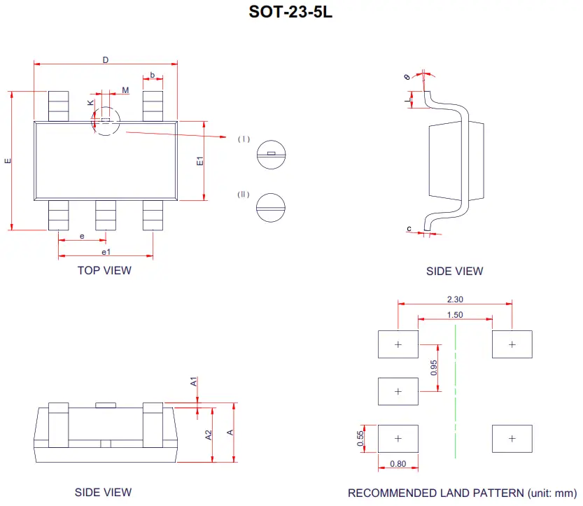
| Symbol | Dimensions in Millimeters | ||
| Min. | Typ. | Max. | |
| A | – | – | 1.45 |
| A1 | 0.00 | – | 0.15 |
| A2 | 0.90 | 1.10 | 1.30 |
| b | 0.30 | 0.40 | 0.50 |
| c | 0.10 | – | 0.21 |
| D | 2.72 | 2.92 | 3.12 |
| E | 2.60 | 2.80 | 3.00 |
| E1 | 1.40 | 1.60 | 1.80 |
| e | 0.95 BSC | ||
| e1 | 1.90 BSC | ||
| L | 0.30 | 0.45 | 0.60 |
| M | 0.10 | 0.15 | 0.25 |
| K | 0.00 | – | 0.25 |
| θ | 0° | – | 8° |
TAPE AND REEL INFORMATION
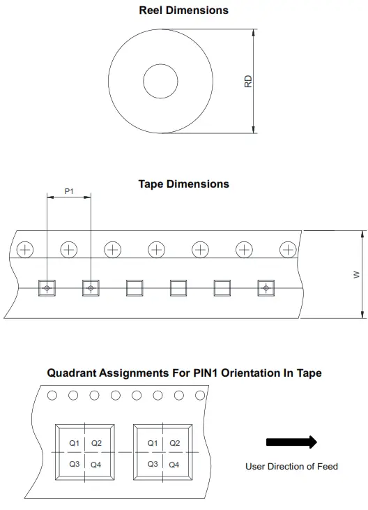
| RD | Reel Dimension | ||||
| W | Overall width of the carrier tape | ||||
| P1 | Pitch between successive cavity centers | ||||
| Pin1 | Pin1 Quadrant | ||||
4275 Burton Drive Santa Clara, CA 95054 USA
Tel: + 1 408 567 3000
Fax: + 1 408 567 3001
www.ovt.com
OmniVision reserves the right to make changes to its products or to discontinue any product or service without further notice.
OmniVision and the OmniVision logo are trademarks or registered trademarks of OmniVision Technologies, Inc.
All other trademarks are the property of their respective owners.


