![]() DS20U Series Quick Guide
DS20U Series Quick Guide
53R-DS20U3-2002 More information on this product can be found at: https://bit.ly/DS20UV2
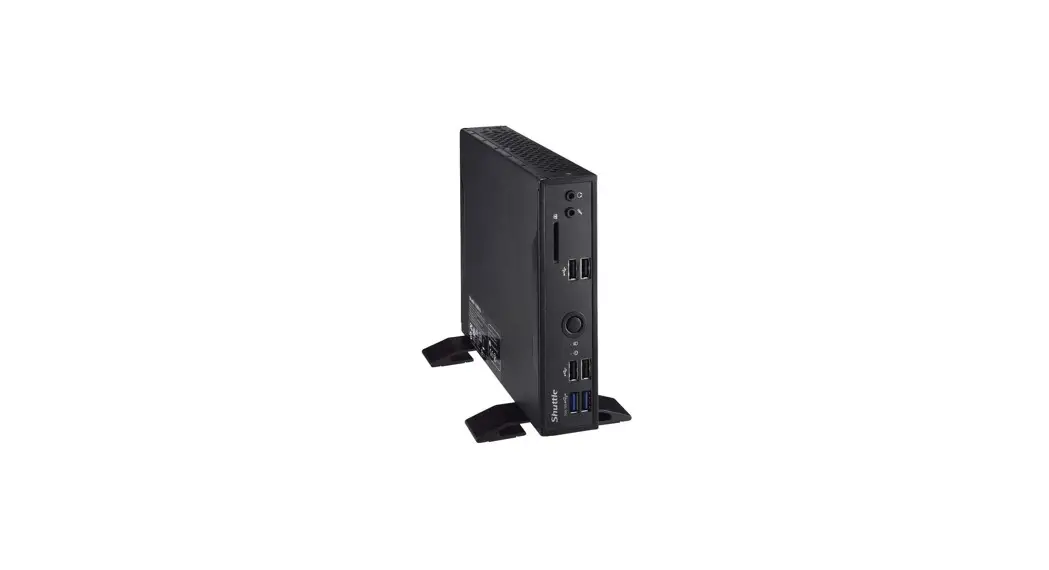
Product Overview
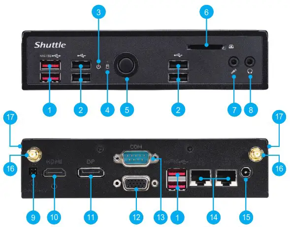
| 1. USB 3.2 Ports (Celeron → Gen 1, Core I → Gen 2) 2. USB 2.0 Ports 3. Power LED 4. Hard Disk Drive LED 5. Power Button 6. SD Card Reader 7. MIC-in 8. Headphones | 9. External Power SW & Clear CMOS 10. HDMI Port 11. DisplayPort 12. COM/VGA Port (RS232 only) (Option) 13. COM Port (RS232/RS422/RS485) (BIOS Setting) 14. LAN Ports 15. Power Jack (DC IN) 16. Connector for WLAN antenna 17. Kensington® Lock Hole |
Hardware Installation
A. Begin Installation![]() For safety reasons, please ensure that the power cord is disconnected before opening the case. !
For safety reasons, please ensure that the power cord is disconnected before opening the case. !
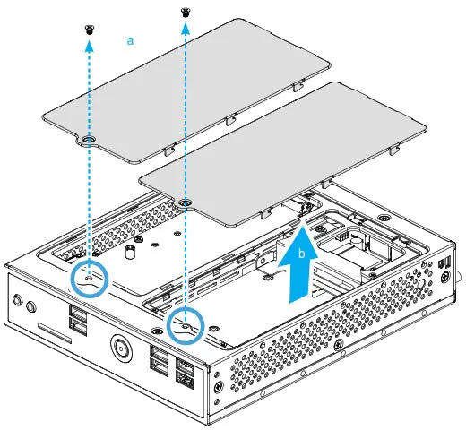
- Unscrew the two screws of the chassis cover. Slide the cover backwards and upwards.

 The product’s colour and specifications may vary from the actually shipping product.
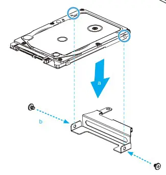
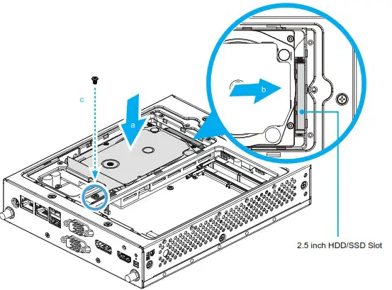
B. HDD or SSD Installation
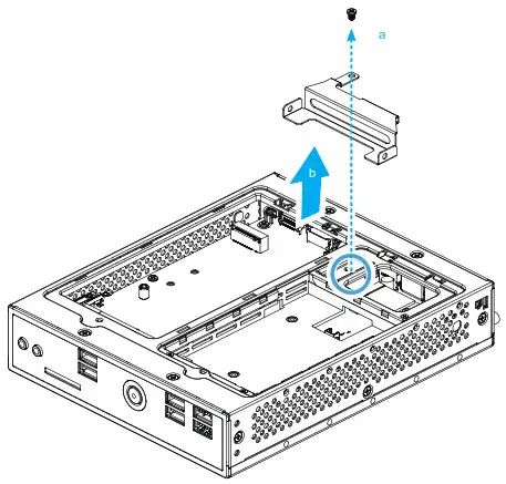
- Unfasten the rack mount screw and remove the rack.

- Place an HDD or SSD in the rack and secure with two screws from each side.

- Lay the HDD or SSD into its drive bay and push it gently to the right until it clicks into place. Refasten screws.

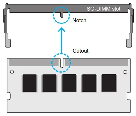
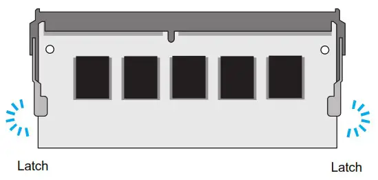
C. Memory Module Installation![]() This motherboard does only support 1.2 V DDR4 SO-DIMM memory modules.
This motherboard does only support 1.2 V DDR4 SO-DIMM memory modules.
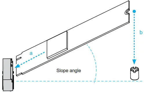
- Locate the SO-DIMM slots on the motherboard.
- Align the notch of the memory module with the one of the relevant memory slot.

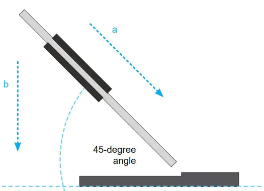
- Gently insert the module into the slot in a 45-degree angle.
- Carefully push down the memory module until it snaps into the locking mechanism.

- Repeat the above steps to install an additional memory module, if required.

D. M.2 Device Installation
- Locate the M.2 key slots on the motherboard.
- Install the M.2 device into the M.2 slot and secure with the screw.
⩥ M.2 2242/2260/2280 M key slot
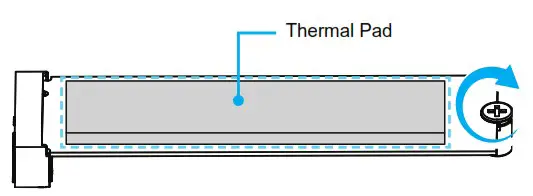
![]() Pasting a thermal pad on the M.2 SSD can effectively reduce its temperature.
Pasting a thermal pad on the M.2 SSD can effectively reduce its temperature.
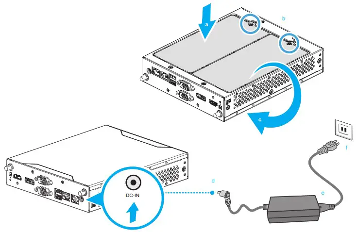
E. Complete
- Please replace and affix the case cover with two screws. Turn your DS20U upside down.
- Connect the power cord.
- Complete.
![]() Please press the “Del” key while booting to enter BIOS. Here, please load the optimised BIOS settings.
Please press the “Del” key while booting to enter BIOS. Here, please load the optimised BIOS settings.
Operation Position: Please make sure to use either the supplied feet or the VESA mount.
Safety Information
![]() Incorrectly replacing the battery may damage this computer. Replace only with the same or equivalent as recommended by Shuttle. Dispose of used batteries according to the manufacturer’s instructions.
Incorrectly replacing the battery may damage this computer. Replace only with the same or equivalent as recommended by Shuttle. Dispose of used batteries according to the manufacturer’s instructions.
![]()
![]()
All bundled parts, power cord included, shall not be used without this product
This device complies with Part 15 of the FCC Rules. Operation is subject to the following two conditions: (1) this device may not cause harmful interference, and (2) this device must accept any interference received, including interference that may cause undesired operation.![]() This device meets the requirements for the EU conformity in accordance to the currently valid EU directives.
This device meets the requirements for the EU conformity in accordance to the currently valid EU directives.
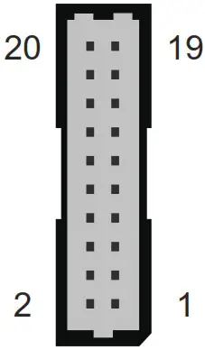
Motherboard Illustration
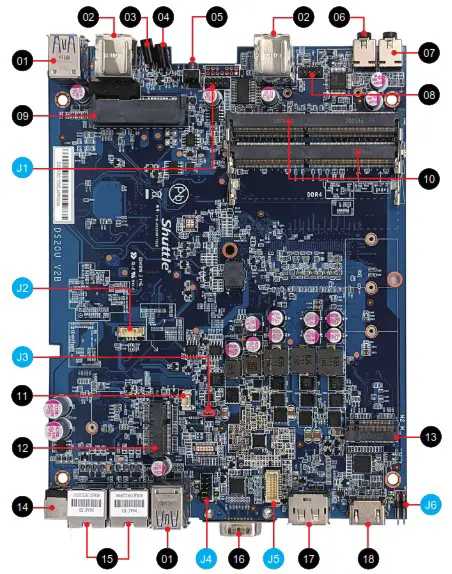 | 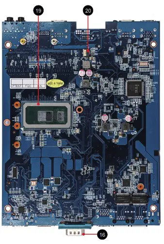 |
| 01. USB 3.2 Ports 02. USB 2.0 Ports 03. Power LED 04. Hard Disk Drive LED 05. Power Button 06. MIC-in 07. Headphones 08. Debug Header 09. 2.5 inch HDD/SSD Slot 10. DDR4 SO-DIMM Slots | 11. Battery Connector 12. M.2 2230 E Key Slot 13. M.2 2242/2260/2280 M key slot 14. Power jack (DC IN) 15. LAN Ports 16. COM Port 17. DisplayPort 18. HDMI Ports 19. Intel® Celeron ® / Pentium processor 20. SD Card Reader FFC Connector – CON3 |
Jumper Settings
J1 COM 2 Port
| COM2 (RS232) | |||
| Pin | Signal Name | Pin | Signal Name |
| 1 | DCD | 2 | RXD |
| 3 | TXD | 4 | DTR |
| 5 | GND | 6 | DSR |
| 7 | RTS | 8 | CTS |
| 9 | RI | ||

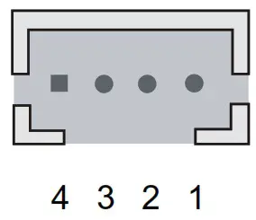
J2 USB 2.0 Connector
| USB5 | |
| Pin | Signal Name |
| 1 | GND |
| 2 | USB_D+ |
| 3 | USB_D- |
| 4 | +5V |
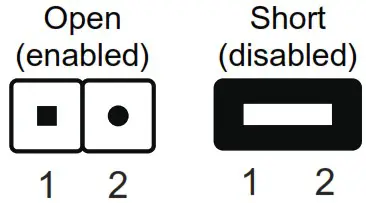
J3 AC Back Auto Power ON
| JP9 | |
| Pin | Signal Name |
| 1 | AM+ |
| 2 | GND |
J4 COM 1 & COM 2 Power Switch
COM PORT Pin 9 “Ring Indicator” (RI) configuration:
| JP1 | |||
| COM1 (pin9) | COM2 (pin9) | ||
| Short Pin | Function | Short Pin | Function |
| 1-2 (Default) | RI1 | 3-4 (Default) | RI2 |
| 5-7 | +5V | 6-8 | +5V |
| 7-9 | +12V | 8-10 | +12V |

J5 VGA connector
| CN6 | |||||
| Pin | Signal Name | Pin | Signal Name | Pin | Signal Name |
| 1 | GND | 2 | GND | 3 | SCL |
| 4 | GND | 5 | SDA | 6 | GND |
| 7 | GND | 8 | GND | 9 | VSYNC |
| 10 | GND | 11 | HSYNC | 12 | GND |
| 13 | GND | 14 | GND | 15 | BOUT |
| 16 | +5V | 17 | GOUT | 18 | +5V |
| 19 | ROUT | 20 | +5V | ||
J6 External Power SW & Clear CMOS
| SW2 | |||
| Pin | Signal Name | Pin | Signal Name |
| 1 | PWRSW- | 2 | +5V |
| 3 | GND | 4 | RTCRST- |

![]()


