National Semiconductor LM741 Amplifier
General Description
The LM741 series are general-purpose operational amplifiers that feature improved performance over industry standards like the LM709. They are direct, plug-in replacements for the 709C, LM201, MC1439 and 748 in most applications. The amplifiers offer many features which make their application nearly foolproof: overload protection on the input and output, no latch-up when the common mode range is exceeded , as well as freedom from oscillations. The LM741C/LM741E are identical to the LM741/LM741A except that the LM741C/LM741E have their performance guaranteed over a 0![]() C to a70
C to a70![]() C temperature range, instead of b55
C temperature range, instead of b55![]() C to a125
C to a125![]() C.
C.
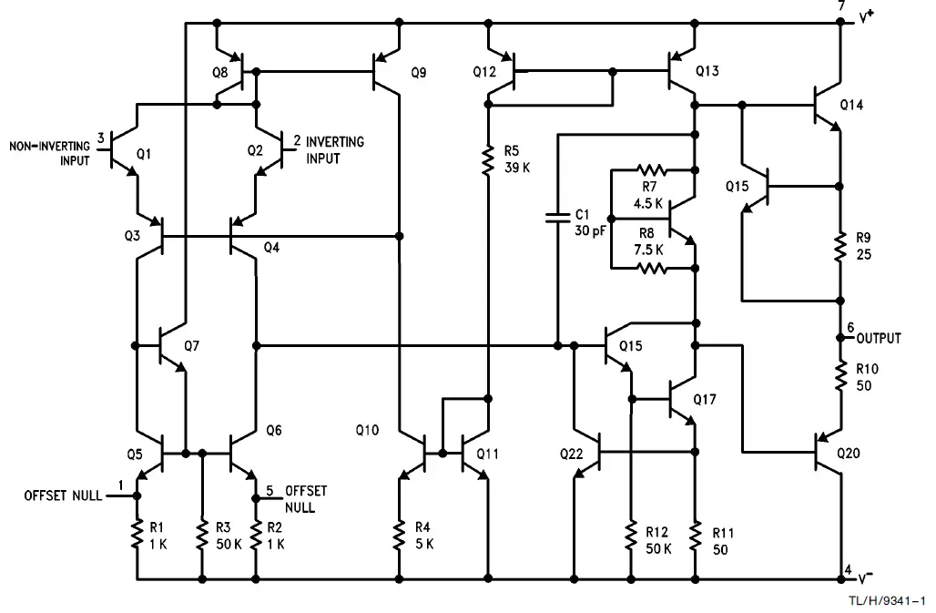
Schematic Diagram
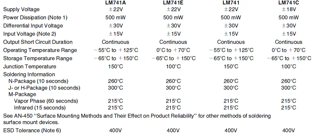
Absolute Maximum Ratings
If Military/Aerospace specified devices are required, please contact the National Semiconductor Sales Office/ Distributors for availability and specifications.
(Note 5)
Electrical Characteristics (Note 3)
| Parameter | Conditions | LM741A/LM741E | LM741 | LM741C | Units | ||||||
| Min | Typ | Max | Min | Typ | Max | Min | Typ | Max | |||
| Input Offset Voltage | TA e 25°C RS s 10 kX RS s 50X |
0.8 |
3.0 | 1.0 | 5.0 | 2.0 | 6.0 | mV mV | |||
| TAMIN s TA s TAMAX RS s 50X RS s 10 kX | 4.0 |
6.0 |
7.5 | mV mV | |||||||
| Average Input Offset Voltage Drift | 15 | mV/°C | |||||||||
| Input Offset Voltage Adjustment Range | TA e 25°C, VS e g20V | g10 | g15 | g15 | mV | ||||||
| Input Offset Current | TA e 25°C | 3.0 | 30 | 20 | 200 | 20 | 200 | nA | |||
| TAMIN s TA s TAMAX | 70 | 85 | 500 | 300 | nA | ||||||
| Average Input Offset Current Drift | 0.5 | nA/°C | |||||||||
| Input Bias Current | TA e 25°C | 30 | 80 | 80 | 500 | 80 | 500 | nA | |||
| TAMIN s TA s TAMAX | 0.210 | 1.5 | 0.8 | mA | |||||||
| Input Resistance | TA e 25°C, VS e g20V | 1.0 | 6.0 | 0.3 | 2.0 | 0.3 | 2.0 | MX | |||
| TAMIN s TA s TAMAX, VS e g20V | 0.5 | MX | |||||||||
| Input Voltage Range | TA e 25°C | g12 | g13 | V | |||||||
| TAMIN s TA s TAMAX | g12 | g13 | V | ||||||||
| Large Signal Voltage Gain | TA e 25°C, RL t 2 kX | ||||||||||
| VS e g20V, VO e g15V | 50 | V/mV | |||||||||
| VS e g15V, VO e g10V | 50 | 200 | 20 | 200 | V/mV | ||||||
| TAMIN s TA s TAMAX, | |||||||||||
| RL t 2 kX, | |||||||||||
| VS e g20V, VO e g15V | 32 | V/mV | |||||||||
| VS e g15V, VO e g10V | 25 | 15 | V/mV | ||||||||
| VS e g5V, VO e g2V | 10 | V/mV | |||||||||
| Parameter | Conditions | LM741A/LM741E | LM741 | LM741C | Units | ||||||
| Min | Typ | Max | Min | Typ | Max | Min | Typ | Max | |||
| Output Voltage Swing | VS e g20V RL t 10 kX RL t 2 kX | g16 g15 | V V | ||||||||
| VS e g15V RL t 10 kX RL t 2 kX | g12 g10 | g14 g13 | g12 g10 | g14 g13 | V V | ||||||
| Output Short Circuit Current | TA e 25°C TAMIN s TA s TAMAX | 10 10 | 25 | 35 40 | 25 | 25 | mA mA | ||||
| Common-Mode Rejection Ratio | TAMIN s TA s TAMAX RS s 10 kX, VCM e g12V RS s 50X, VCM e g12V |
80 |
95 | 70 | 90 | 70 | 90 | dB dB | |||
| Supply Voltage Rejection Ratio | TAMIN s TA s TAMAX, VS e g20V to VS e g5V RS s 50X RS s 10 kX |
86 |
96 |
77 |
96 |
77 |
96 |
dB dB | |||
| Transient Response | TA e 25°C, Unity Gain | ||||||||||
| Rise Time | 0.25 | 0.8 | 0.3 | 0.3 | ms | ||||||
| Overshoot | 6.0 | 20 | 5 | 5 | % | ||||||
| Bandwidth (Note 4) | TA e 25°C | 0.437 | 1.5 | MHz | |||||||
| Slew Rate | TA e 25°C, Unity Gain | 0.3 | 0.7 | 0.5 | 0.5 | V/ms | |||||
| Supply Current | TA e 25°C | 1.7 | 2.8 | 1.7 | 2.8 | mA | |||||
| Power Consumption | TA e 25°C | ||||||||||
| VS e g20V | 80 | 150 | mW | ||||||||
| VS e g15V | 50 | 85 | 50 | 85 | mW | ||||||
| LM741A | VS e g20V | ||||||||||
| TA e TAMIN | 165 | mW | |||||||||
| TA e TAMAX | 135 | mW | |||||||||
| LM741E | VS e g20V | ||||||||||
| TA e TAMIN | 150 | mW | |||||||||
| TA e TAMAX | 150 | mW | |||||||||
| LM741 | VS e g15V | ||||||||||
| TA e TAMIN | 60 | 100 | mW | ||||||||
| TA e TAMAX | 45 | 75 | mW | ||||||||
Note 1: For operation at elevated temperatures, these devices must be derated based on thermal resistance, and Tj max. (listed under ‘‘Absolute Maximum Ratings’’). Tj =TA + (ojA PD).
| Thermal Resistance | Cerdip (J) | DIP (N) | HO8 (H) | SO-8 (M) |
| ojA (Junction to Ambient) | 100°C/W | 100°C/W | 170°C/W | 195°C/W |
| ojC (Junction to Case) | N/A | N/A | 25°C/W | N/A |
Note 2: For supply voltages less than g15V, the absolute maximum input voltage is equal to the supply voltage.
Note 3: Unless otherwise specified, these specifications apply for VS e g15V, b55![]() C s TA s a125
C s TA s a125![]() C (LM741/LM741A). For the LM741C/LM741E, these specifications are limited to 0
C (LM741/LM741A). For the LM741C/LM741E, these specifications are limited to 0![]() C s TA s a70
C s TA s a70![]() C.
C.
Note 4: Calculated value from: BW (MHz) e 0.35/Rise Time(ms).
Note 5: For military specifications see RETS741X for LM741 and RETS741AX for LM741A.
Note 6: Human body model, 1.5 kX in series with 100 pF.
Connection Diagrams
Metal Can Package
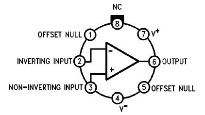
- Order Number: LM741H, LM741H/883, LM741AH/883 or LM741CH
- See NS Package Number H08C
Ceramic Dual-In-Line Package
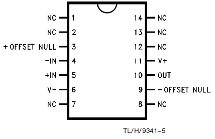
- Order Number LM741J-14/883*, LM741AJ-14/883
- See NS Package Number J14A
- also available per JM38510/10101
- also available per JM38510/10102
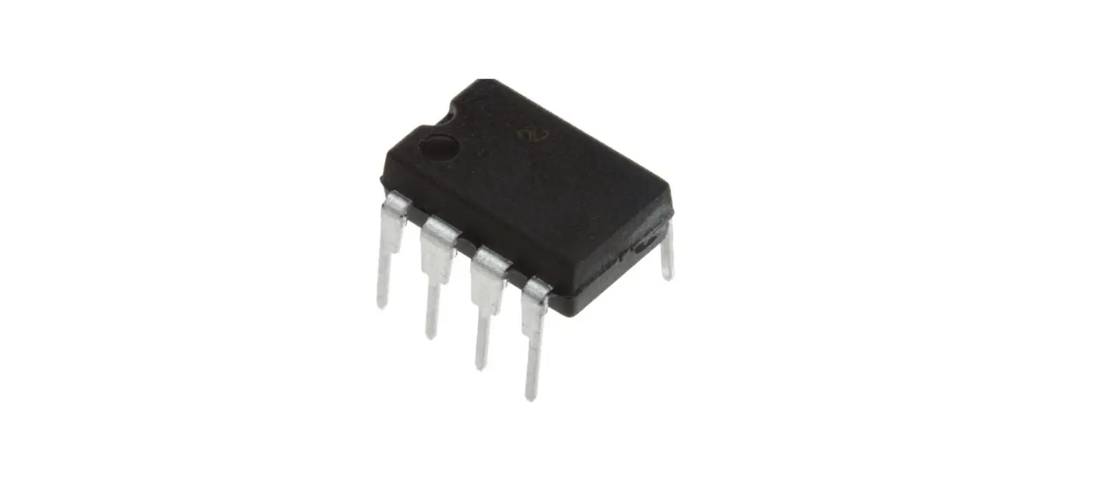
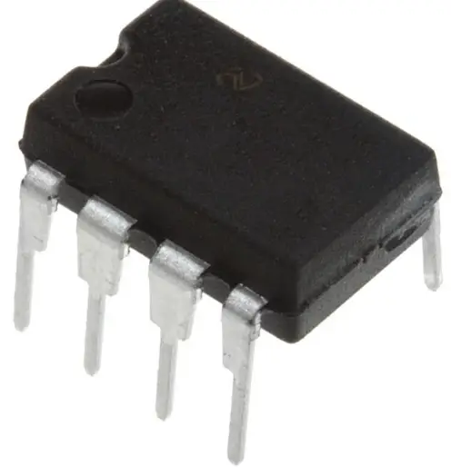
Dual-In-Line or S.O. Package
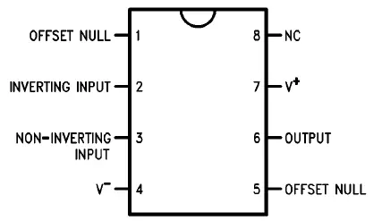
- Order Number LM741J, LM741J/883, LM741CM, LM741CN or LM741EN
- See NS Package Number J08A, M08A or N08E
Ceramic Flatpak
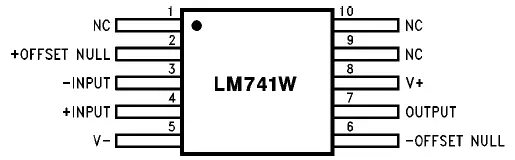
- Order Number LM741W/883 See NS Package Number W10A
Physical Dimensions inches (millimeters)
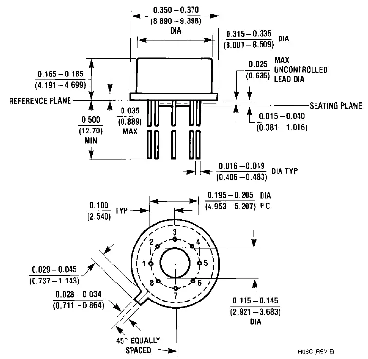
- Metal Can Package (H)
- Order Number LM741H, LM741H/883, LM741AH/883, LM741CH or LM741EH NS Package Number H08C


