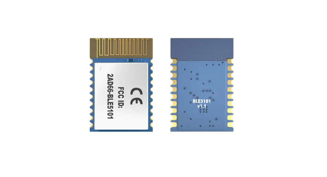
![]() MPRFMODULE1 2.4G Proprietary BLE Module
MPRFMODULE1 2.4G Proprietary BLE Module
Instruction Manual
Revision history
| Version | Date | Description |
| 1.0 | 2022/5/22 | First release |
| 1.1 | 2022/8/22 | RF warning message |
| 1.2 | 2022/8/22 | RF warning message update |
| 1.3 | 2022/8/22 | RF info update |
| 1.4 | 2022/09/06 | Add ch4 antenna instructions |
| 1.5 | 2022/10/04 | Add 5.2 – 5.4 for FCC/IC requirement |
Product Introduction
1.1 Introduction
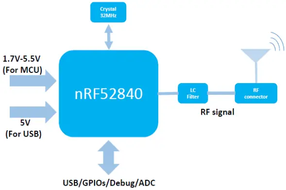
MPRFMODULE1 is a BLE 5.2/ 2.4G proprietary module based on Nordic nRF52840 SoC with a 32-bit ARM ® ® Cortex M4 CPU, 1MB flash, and 256kB RAM. The module comes with a coaxial connector for an external PIFA antenna.
1.2 Feather
- ARM ® Cortex ® M4 32bit processor with FPU, 64Mhz
- 1 MB flash and 256 kB RAM
- Bluetooth ® 5 & 2.4 GHz transceiver
- BLE 5 data rate: 1 Mbps
- 2.4G proprietary data rate: 2 Mbps
- Flexible power management: 1.7V to 5.5V supply voltage range
On-chip DC/DC and LDO regulators with automated low current modes 1.8V to 3.3V regulated supply for external components
1.3 Certification
- FCC ID:
- CE IDL:
- DID:
Product Descriptions
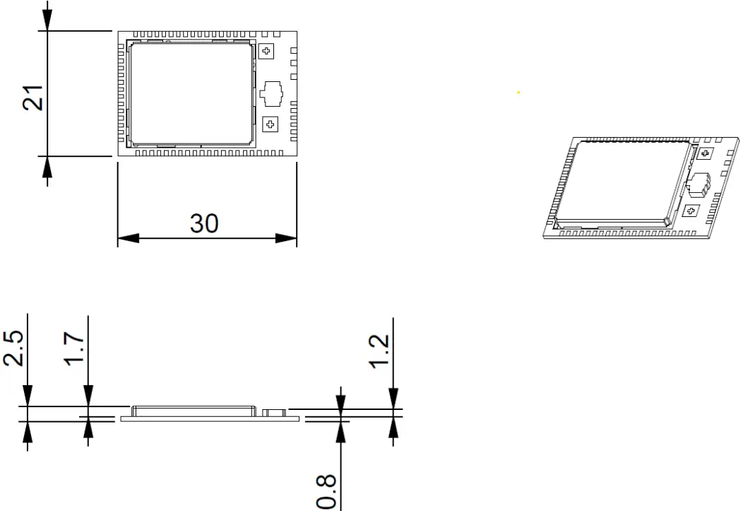
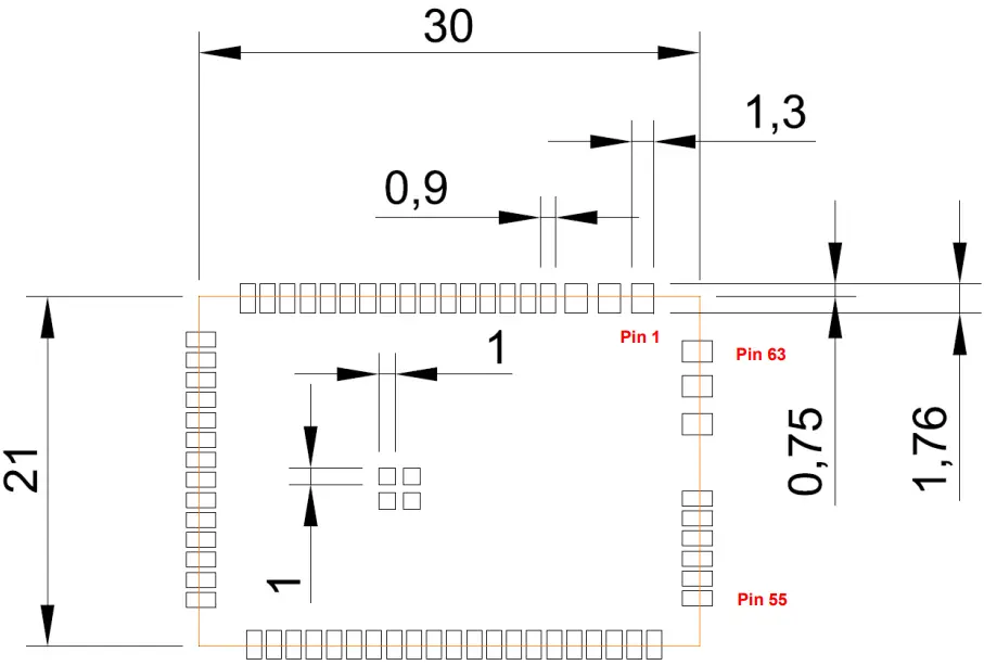
2.1 Dimension
- PCB Size: 21 x 30 x 0.8mm

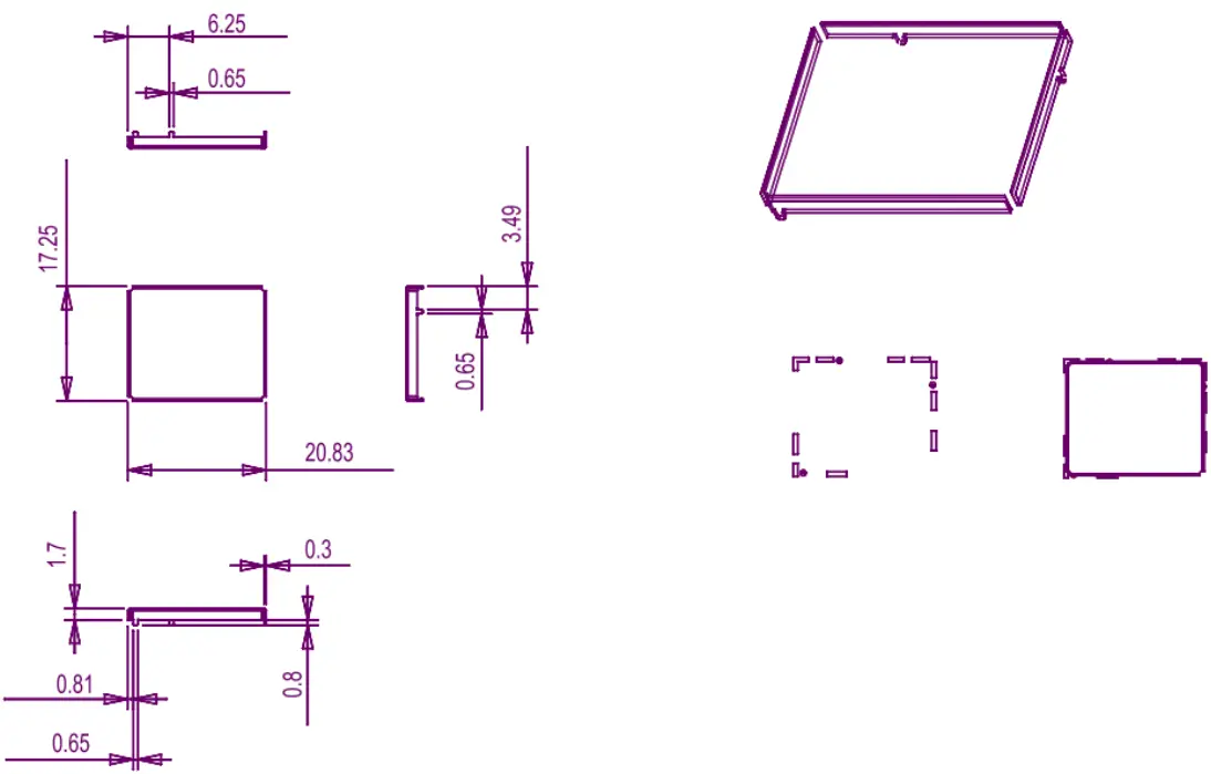
- Shielding Case

2.2 Pin definition
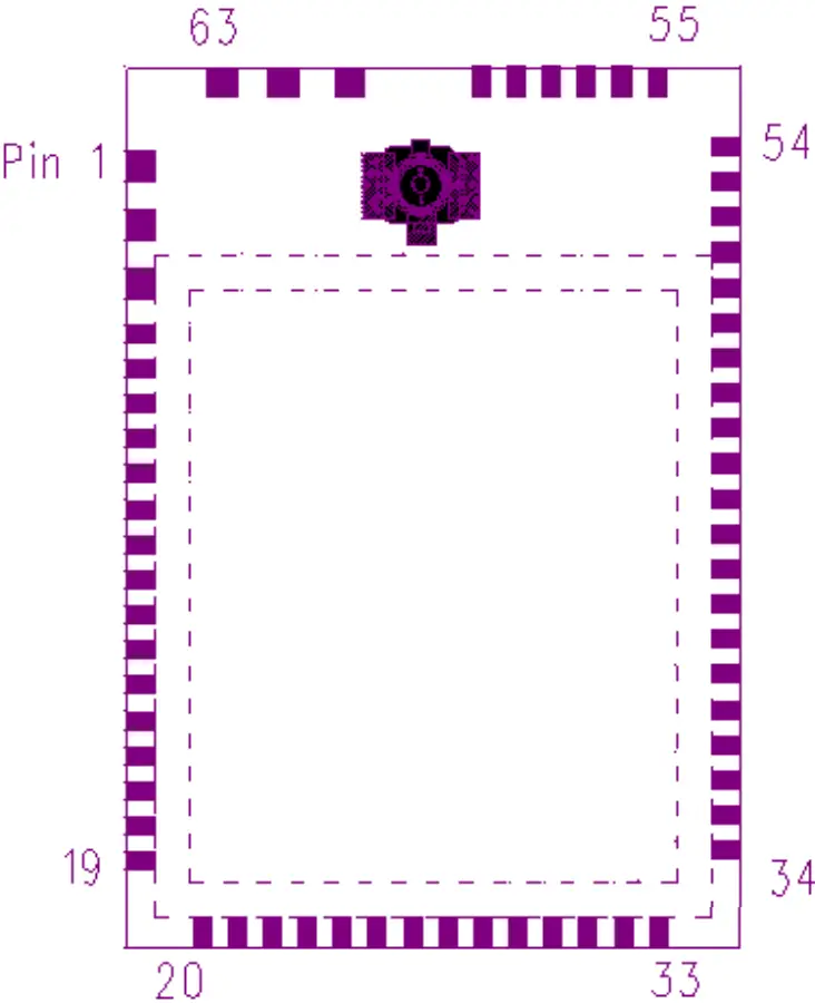
| Pin No. | Name | Function | Description |
| 1 | GND | Power | ground |
| 2 | GND | Power | ground |
| 3 | GND | Power | ground |
| 4 | P1.11 | Digital I/O | General purpose I/O (Standard drive) |
| 5 | P1.12 | Digital I/O | General purpose I/O (Standard drive) |
| 6 | P1.14 | Digital I/O | General purpose I/O (Standard drive) |
| 7 | P0.03 | Digital I/O Analog input | General purpose I/O (Standard drive) Analog input |
| 8 | P0.28 | Digital I/O Analog input | General purpose I/O (Standard drive) Analog input |
| 9 | P1.10 | Digital I/O | General purpose I/O (Standard drive) |
| 10 | P1.13 | Digital I/O | General purpose I/O (Standard drive) |
| 11 | P1.15 | Digital I/O | General purpose I/O (Standard drive) |
| 12 | P0.02 | Digital I/O Analog input | General purpose I/O (Standard drive) Analog input |
| 13 | P0.29 | Digital I/O Analog input | General purpose I/O (Standard drive) Analog input |
| 14 | P0.31 | Digital I/O Analog input | General purpose I/O (Standard drive) Analog input |
| 15 | P0.30 | Digital I/O Analog input | General purpose I/O (Standard drive) Analog input |
| 16 | P0.27 | Digital I/O | General purpose I/O |
| 17 | P0.05 | Digital I/O Analog input | General purpose I/O Analog input |
| 18 | P0.07 | Digital I/O | General purpose I/O |
| 19 | P1.08 | Digital I/O | General purpose I/O |
| 20 | P0.11 | Digital I/O | General purpose I/O |
| 21 | P0.00 | Digital I/O Analog input | General purpose I/O Analog input |
| 22 | P0.01 | Digital I/O Analog input | General purpose I/O Analog input |
| 23 | P0.26 | Digital I/O | General purpose I/O |
| 24 | P0.04 | Digital I/O Analog input | General purpose I/O Analog input |
| 25 | P0.06 | Digital I/O | General purpose I/O |
| 26 | P0.08 | Digital I/O | General purpose I/O |
| 27 | P1.09 | Digital I/O | General purpose I/O |
| 28 | P0.12 | Digital I/O | General purpose I/O |
| 29 | VDDH | Power | High voltage power supply |
| 30 | DCCH | Power | DC/DC converter output |
| 31 | VBUS | power | 5 V input for USB 3.3 V regulator |
| 32 | VDD | power | Power supply |
| 33 | GND | power | ground |
| 34 | P0.14 | Digital I/O | General purpose I/O |
| 35 | D- | USB | USB D- |
| 36 | D+ | USB | SUB D+ |
| 37 | P0.16 | Digital I/O | General purpose I/O |
| 38 | P0.18 | Digital I/O | General purpose I/O |
| 39 | P0.19 | Digital I/O | General purpose I/O |
| 40 | P0.13 | Digital I/O | General purpose I/O |
| 41 | P0.15 | Digital I/O | General purpose I/O |
| 42 | P0.17 | Digital I/O | General purpose I/O |
| 43 | P0.21 | Digital I/O | General purpose I/O |
| 44 | P0.20 | Digital I/O | General purpose I/O |
| 45 | P0.22 | Digital I/O | General purpose I/O |
| 46 | P0.24 | Digital I/O | General purpose I/O |
| 47 | P1.00 | Digital I/O | General purpose I/O |
| 48 | SWDIO | Debug | Serial wire debug I/O for debugging and programming |
| 49 | SWDCLK | Debug | Serial wire debug clock input for debugging and programming |
| 50 | P1.02 | Digital I/O | General purpose I/O (Standard drive) |
| 51 | P1.04 | Digital I/O | General purpose I/O (Standard drive) |
| 52 | P1.06 | Digital I/O | General purpose I/O (Standard drive) |
| 53 | P0.09 | Digital I/O | General purpose I/O (Standard drive) |
| 54 | P0.10 | Digital I/O | General purpose I/O (Standard drive) |
| 55 | P0.23 | Digital I/O | General purpose I/O |
| 56 | P0.25 | Digital I/O | General purpose I/O |
| 57 | P1.01 | Digital I/O | General purpose I/O (Standard drive) |
| 58 | P1.03 | Digital I/O | General purpose I/O (Standard drive) |
| 59 | P1.05 | Digital I/O | General purpose I/O (Standard drive) |
| 60 | P1.07 | Digital I/O | General purpose I/O (Standard drive) |
| 61 | GND | Power | ground |
| 62 | GND | Power | ground |
| 63 | GND | Power | ground |
2.3 Footprint
2.4 Block diagram
Electrical specification
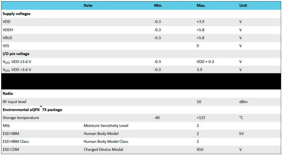
3.1 Absolute maximum ratings
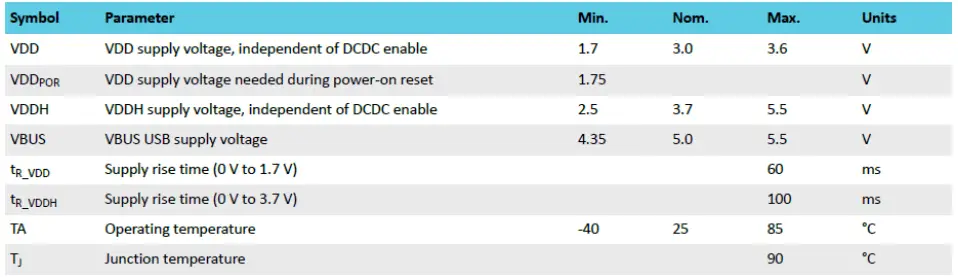
3.2 Recommended operating conditions
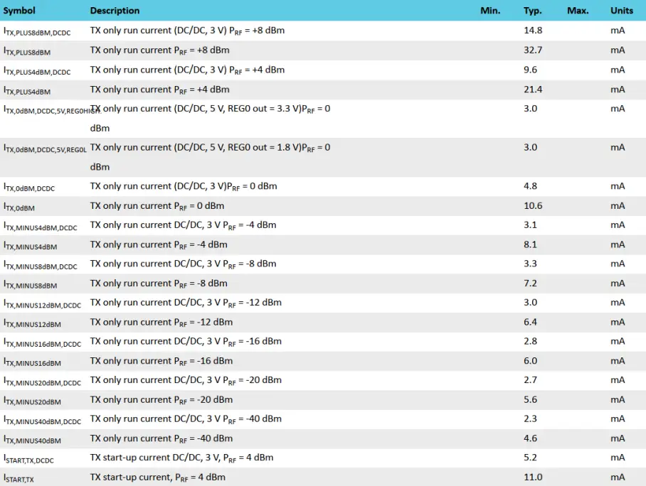
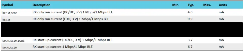
3.3 General radio characteristics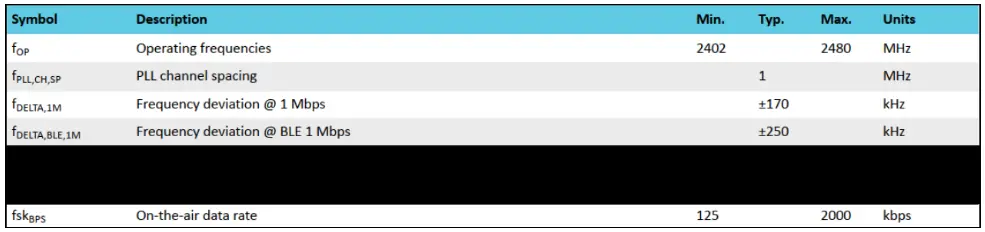 3.4 Radio current consumption (transmitter)
3.5 Radio current consumption (Receiver)
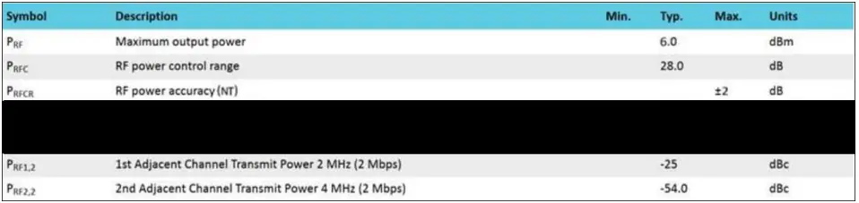
3.6 Transmitter specification
3.7 Receiver operation
¹ Typical sensitivity applies when ADDRO is used for receiver address correlation. When ADDR[1…7] is used for receiver address correlation, the typical sensitivity for this mode is degraded by 3 dB.
² Typical sensitivity applies when ADDRO is used for receiver address correlation. When ADDR[1..7] is used for receiver address correlation, the typical sensitivity for this mode is degraded by 3 dB.
³ As defined in the Bluetooth Core Specification v4.0 Volume 6: Core System Package (Low Energy Controller Volume) 4 Equivalent BER limit < 10E-04
3.8 RX selectivity5
 5 Desired signal level at PIN = -67 dBm. One interferer is used, having equal modulation as the desired signal. The input power of the interferer where the sensitivity equals BER = 0.1% is presented
3.9 RX intermodulation6
6 Desired signal level at PIN = -64 dBm. Two interferers with equal input power are used. The interferer closest in frequency is not modulated, the other interferer is modulated equally to the desired signal. The input power of the interferers where the sensitivity equals BER = 0.1% is presented.
3.10 Radio timing
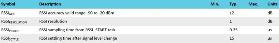
3.11 Received signal strength indicator (RSSI) specifications
Antenna
4.1 Antenna Type and Gains
Only antennas of the same type and with equal or fewer gains as 3.96 dBi for the 2.4GHz band shall be used with the MPRFMODULE1. Other types of antennas and/or higher gain antennas may require additional authorization for operation. For testing purposes the following dual-band antenna approximates closely the above limits used:
| Antenna Type | Part No. | Peak Gain | Length |
| PIFA | 20LT0-000LJ000 | 3.96 dBi for 2.4GHz | 150mm |
| Note: The antenna gain includes cable loss. | |||
4.2 Antenna Placement Within the Host Platform
To ensure RF exposure compliance the antenna used with the ASUS wireless module must be installed in host platforms to provide a minimum separation distance from all persons, in all operating modes and orientations of the host platform, with strict adherence to the table below. The antenna separation distance applies to both the horizontal and vertical orientation of the antenna when installed in the host system.
| ASUS Wireless Module | Minimum required antenna-to-user separation distance |
| MPRFMODULE1 | 0 mm |
4.3 Recommended Method For Retention Of Cable
It is recommended to restrain the antenna cables of products of cable length leaving the RF connectors on the module.
It is recommended to use a robust tape or adhesive to secure the cables so they do not move or pull on the connector during the shock and vibration of the system.
RF warning message
5.1 RF Exposure Information (SAR)
This device meets the government’s requirements for exposure to radio waves. This device is designed and manufactured not to exceed the emission limits for exposure to radio frequency (RF) energy set by the Federal Communications Commission of the U.S. Government.
The exposure standard employs a unit of measurement known as the Specific Absorption Rate or SAR. The SAR limit set by the FCC is 1.6 W/kg. Tests for SAR are conducted using standard operating positions accepted by the FCC with the EUT transmitting at the specified power level in different channels.
The FCC has granted Equipment Authorization for this device with all reported SAR levels evaluated as in compliance with the FCC RF exposure guidelines. SAR information on this device is on file with the FCC and can be found under the Display Grant section of www.fcc.gov/eot/ea/fccid after searching on FCC ID: MSQMPRFMODULE1
5.2 Class B Device Interference Statement
This wireless module has been tested and found to comply with the limits for a Class B digital device, pursuant to Part 15 of the FCC Rules. These limits are designed to provide reasonable protection against harmful interference in a residential installation. This wireless module generates, uses, and can radiate radio frequency energy. If the wireless module is not installed and used in accordance with the instructions, the wireless module may cause harmful interference to radio communications. There is no guarantee, however, that such interference will not occur in a particular installation. If this wireless module does cause harmful interference to radio or television reception (which can be determined by turning the equipment off and on), the user is encouraged to try to correct the interference by taking one or more of the following measures:
- Reorient or relocate the receiving antenna of the equipment experiencing interference.
- Increase the distance between the wireless module and the equipment experiencing interference.
- Connect the computer with the wireless adapter to an outlet on a circuit different from that to which the equipment experiencing the interference is connected.
- Consult the dealer or an experienced radio/TV technician for help.
NOTE: The adapter must be installed and used in strict accordance with the manufacturer’s instructions as described in the user documentation that comes with the product. Any other installation or use will violate FCC Part 15 regulations.
5.3 Information for OEMs and Host Integrators
The guidelines described within this document are provided to OEM integrators installing ASUS wireless modules in keyboard and mouse devices. Adherence to these requirements is necessary to meet the conditions of compliance with FCC rules, including RF exposure. When all antenna type and placement guidelines described herein are fulfilled the ASUS wireless module may be incorporated into keyboard and mouse devices with no further restrictions. If any of the guidelines described herein are not satisfied it may be necessary for the OEM or integrator to perform additional testing and/or obtain additional approval. The OEM or integrator is responsible to determine the required host regulatory testing and/or obtaining the required host approvals for compliance.
- ASUS wireless modules are intended for OEMs and host integrators only.
- The ASUS wireless module FCC Grant of Authorization describes any limited conditions of modular approval.
- The ASUS wireless module must be operated with an access point that has been approved for the country of operation.
- Changes or modification to ASUS wireless module by OEMs, integrators, or other third parties is not permitted. Any changes or modifications to ASUS wireless module by OEMs, integrators, or other third parties will void authorization to operate the adapter.
5.4 Simultaneous Transmission of ASUS Wireless Module with Other Integrated or Plug-In Transmitters
Based upon FCC Knowledge Database publication number 616217, when there are multiple transmitting devices installed in a host device, an RF exposure transmitting assessment shall be performed to determine the necessary application and test requirements. OEM integrators must identify all possible combinations of simultaneous transmission configurations for all transmitters and antennas installed in the host system. This includes transmitters installed in the host as mobile devices (>20 cm separation from the user) and portable devices (<20 cm separation from the user). OEM integrators should consult the actual FCC KDB 616217 document for all details in making this assessment to determine if any additional requirements for testing or FCC approval are necessary.
Canada, Innovation, Science and Economic Development Canada (ISED) Notices
This device contains license-exempt transmitter(s)/receiver(s) that comply with Innovation, Science, and Economic Development Canada’s license-exempt RSS(s). Operation is subject to the following two conditions:
- This device may not cause interference.
- This device must accept any interference, including interference that may cause undesired operation of the device.
Radio Frequency (RF) Exposure Information
The radiated output power of the Wireless Device is below the Innovation, Science, and Economic Development Canada (ISED) radio frequency exposure limits. The Wireless Device should be used in such a manner that the potential for human contact during normal operation is minimized.
This device has been evaluated for and shown compliant with the ISED Specific Absorption Rate (“SAR”) limits when operated in portable exposure conditions.
Antenna List
| No. | Manufacturer | Part No. | Antenna Type | Peak Gain |
| 1 | ASUS | 20LT0-000LJ000 (Main) | PIFA | 3.96 dBi for 2.4 GHz |
CE RED RF Output table (Directive 2014/53/EU)
| Function | FREQUENCY | Maximum Output Power(EIRP) |
| WiFi | 2402-2480 MHz | 10 dBm |
| Bluetooth | 2402-2480 MHz | 10 dBm |
UKCA RF Output table (The Radio Equipment Regulations 2017)
| Function | FREQUENCY | Maximum Output Power(EIRP) |
| WiFi | 2402-2480 MHz | 10 dBm |
| Bluetooth | 2402-2480 MHz | 10 dBm |
KC RF Output Table
| Function | Frequency | Power |
| 2.4GHz wireless | 2402-2480MHz-Module | 4mW |
| BLE | 2402-2480MHz-Module | 4mW |
| Manufacturer | ASUSTek COMPUTER INC. |
| Address, City | 1 F., No. 15, Lide Rd., Beitou Dist., Taipei City 112, Taiwan |
| Authorized Representative in Europe | ASUS COMPUTER GmbH |
| Address | Harkortstrasse 21-23, 40880 Ratingen |
| Country | Germany |
| Authorized Representative in the United Kingdom | ASUSTEK (UK) LIMITED |
| Address | 1st Floor, Sackville House, 143-149 Fenchurch Street, London, EC3M 6BL, England |
| Country | United Kingdom |
![]()


