![]()
M.2-B048-101
FII Industrial PCIE M.2 Module
Product specification V1.0
| Project Name | Sirisu Fly mPro |
| Module Code | M.2-B048-101 |
Customer Approval: _________________
Revision history
| Version | Date | Author | Modification |
| V1.0 | 11-08-20 | ||
Product Overview
The M.2-B048-101 PCIE M.2 data module is a PCI Express M.2 data module based on the LTE (Long Term Evolution) standard. It is mainly used by industry customers for secondary terminal development. The module is integrated into the terminal and used as an LTE Modem to provide a wireless data interface to realize the air interface data transmission function. The main features are as follows:
- Flexible in use, easy to build an industry terminal industry chain, and quickly realize LTE trunking services and data services
- Support 3GPP Release 12
- Support QPSK, 16QAM, 64QAM
- Provide serial port, USB, SDIO3.0, PCIE data transmission interface
- Support Linux embedded operating system
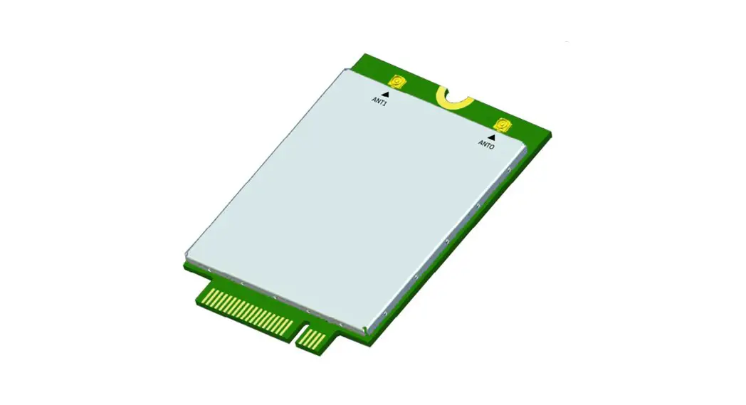
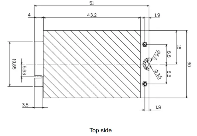
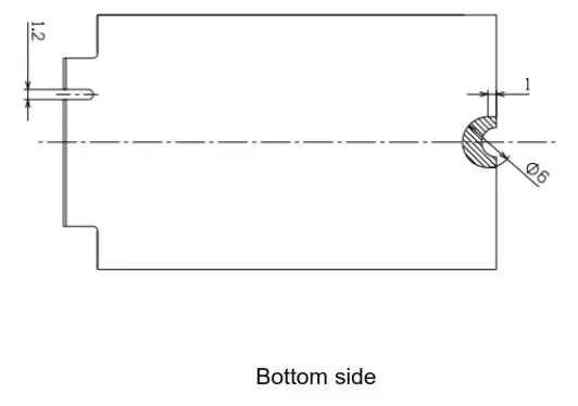
The appearance and physical dimensions of M.2-B048-101 are shown in Figure 1-1 and Figure 1-2 (please refer to the actual product).
Figure 1-1 Schematic diagram of the appearance of M.2-B048-101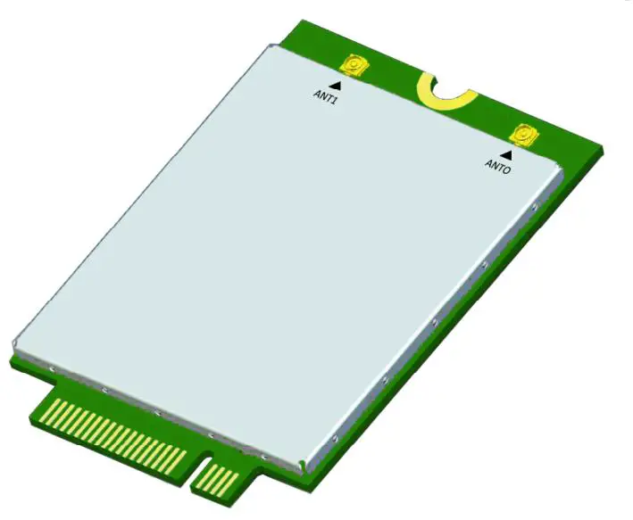
Figure 1-2 Physical dimensions of M.2-B048-101 module
Electrical technical indicators
Electrical characteristics
| Item | Description |
| Size | 51x30x4.75mm (LxWxH) |
| Weight | ≤20g |
| Interface | Communication: USB 2.0. USB 3.0. SDIO 3.0. PCIE 3.0 Power: 3.3V DC USIM: Support USIM UART: One 2-wire UART&One 4-wire UART Wakeup: Can be waked up |
| Antenna Port | 2 Antenna Port 500 |
| Operating temperature | -20°C— +55°C |
| Storage temperature | -40°C— +85°C |
| Frequency band | B48(3550-3700MHz) |
| Channel Bandwidth | 5MHz/10MHz/15MHz/20MHz |
| Rated Output Power | 15.5dBm (t2dB) |
| Sensitivity | ≤5-99dBm (5MHz) ≤5-96dBnn (10MHz) ≤5-94.2dBm (15MHz) ≤5-93dBm (20MHz) |
| Power | DC: 3.3V |
| RoHS | Comply with RoHS environmental certification requirements |
Module Interface
The module interface is PCIE M.2 interface, as shown in Figure 2-1
Figure 2-1 Physical dimensions of PCIE M.2 Interface
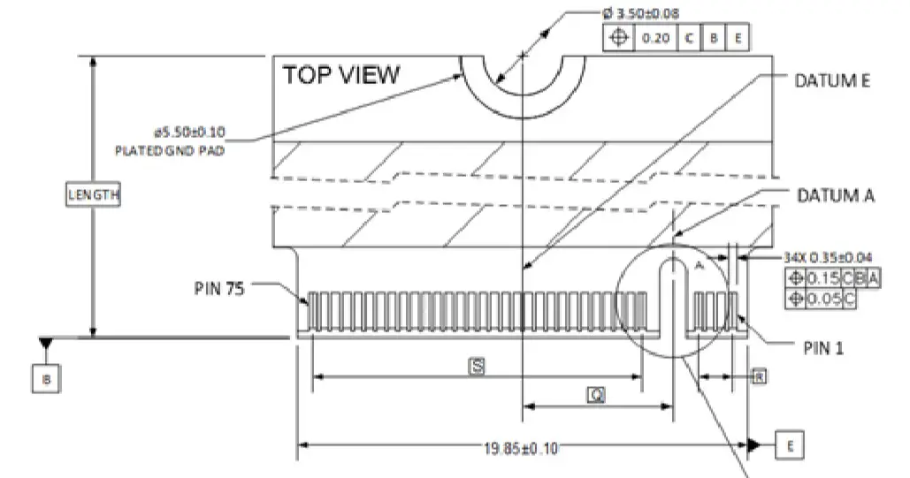
Pin definition
The pin definition of the module interface is shown in Table 2-1.
Table 2-1 PCIE M.2 interface pin definition
| Pin | Defination | Function | Pin | Defination | Function |
| 75 | CONFIG_2 (GND) | ||||
| 74 | 3.3V | 73 | GND | ||
| 72 | 3.3V | 71 | GND | ||
| 70 | 3.3V | 69 | CONFIG_1 (GND) | ||
| 68 | 32.768KHz | 32.768KHz | 67 | RESET# (I)(0/1.8V) | |
| 66 | SIM DETECT | 65 | SDHO CMD | SDIO CMD | |
| 64 | UARTO TX | UARTO | 63 | GPIO (I/0)(0/1.8V) | |
| 62 | UARTO RX | 61 | GPIO (I/0)(0/1.8V) | ||
| 60 | GPIO (I/0)(0/1.8V) | PCIE ENABLE | 59 | GPIO (1/0)(0/1.8V) | |
| 58 | NC/UART1 TX | Option UART1 | 57 | GND | |
| 56 | NC/UART1 RX | 55 | REFCLKP | PCIE REFCLK | |
| 54 | PEWAKE# (I0)(0/3.3V) | 53 | REFCLKN | ||
| 52 | CLKREQ# (I0)(0/3.3V) | 51 | GND | ||
| 50 | PERST# (I)(0/3.3V) | 49 | PERpO | PCIE RXO | |
| 48 | SDHO DO | SDIO Data and Clk | 47 | PERnO | |
| 46 | SDHO D1 | 45 | GND | ||
| 44 | SDHO D2 | 43 | PETpO | PCIE TXO | |
| 42 | SDHO D3 | 41 | PETnO | ||
| 40 | SDHO CLK | 39 | GND | ||
| 38 | NC/GPIO (I/0)(0/1.8V) | Option GPIO | 37 | USB3.0-Rx+ | USB3.0-RX |
| 36 | UIM 1 -PWR (0) | USIM 1 | 35 | USB3.0-Rx- | |
| 34 | UIM 1-DATA (10) | 33 | GND | ||
| 32 | UIM 1-CLK (0) | 31 | USB3.0-Tx+ | USB3.0-TX | |
| 30 | UIM 1 -RESET (0) | 29 | USB3.0-Tx- | ||
| 28 | UART2 CTS(0/1.8V) | UART2 | 27 | GND | |
| 26 | UART2 RTS(0/1.8V) | 25 | GPIO (I/0)(0/1.8V) | ||
| 24 | UART2 RXD(0/1.8V) | 23 | GPIO- WoWWAN# (0)(0/1.8V) | ||
| 22 | UART2 TXD (0)(0/1.8V) | 21 | CONFIG_0 (NC) | ||
| 20 | GPIO (I/0)(0/1.8V) | 19 | / | ||
| 18 | / | 17 | / | ||
| 16 | / | 15 | / | ||
| 14 | / | 13 | / | ||
| 12 | / | 11 | GND | ||
| 10 | GPIO-LED#1 (0) | 9 | USB D- | USB2.0 | |
| 8 | W DISABLE1# (I)(0/3.3V) | 7 | USB D+ | ||
| 6 | FULL CARD POWER OFF# — (I)(5/3.3V — | 5 | GND | ||
| 4 | 3.3V | 3 | GND | ||
| 2 | 3.3V | 1 | CONFIG_3 (NC) |
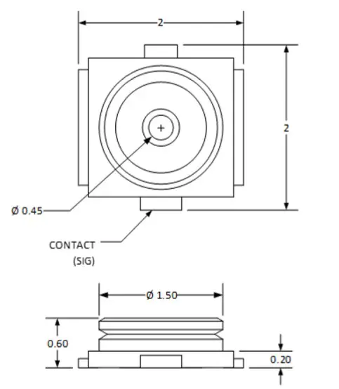
RF connector
The size of the connector is shown in Figure 2-2
Figure 2-2 Schematic diagram of the physical size of the radio frequency connector (IPEX)
Thermal Design
In the installation design integrated into the industry equipment, in order to ensure the stability and reliability of the M.2-B048-101 module, it is necessary to pay attention to the heat dissipation design of the module. The main heat dissipation measures are as follows:
- The PCB board does not need to be hollowed out.
- The recommended minimum thermal conductivity of the thermal conductive material is
3W/m-k for heat dissipation between the module and the user’s bottom board through the thermal pad pressing. The size of the thermal pad is 42mm x 29.4mm. The height of the thermal pad is determined by the height of the PCIE M.2 connector selected by the user and the installation method of the module. When determining the height of the thermal pad, it is recommended to follow the following rules: After the module is connected to the user base, the compression ratio of the thermal pad is 15% to 30% of the size of the thermal pad. Refer to Figure 3-1 below, the height reference value is 2mm.
Figure 3-1 Schematic diagram of M.2-B048-101 module before installation
- A screw hole is reserved on the user backplane to connect to the ground plane of the backplane. When installing the module, tighten a metal screw to fix the module to the user backplane. Refer to Figure 3-2 below.
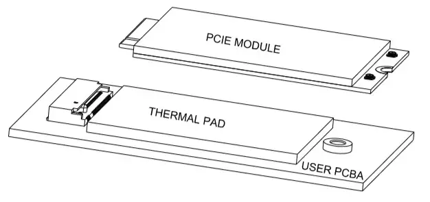
Figure 3-2 Schematic diagram of M.2-B048-101 module after installation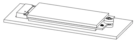
Strengthen the air flow around the module. Try not to place any parts on the module projection area of the user backplane. Do not place heat sensitive components (such as crystals) or any other components that consume 1.5W or higher power around the module. Choose a large user baseboard. The thermal pad between the module and the user backplane can improve the heat dissipation performance of the multilayer backplane. Cover the installation area of the thermal pad on the user baseboard with copper. Use continuous ground planes on the user backplane as much as possible, and holes must be used to connect between ground planes. Therefore, reserve as many holes as possible.
Product List
| Product Name | QTY | Remark |
| M.2-B048-101 | 01-01-00 | Default |
List of Abbreviations
| Abbreviation | Full Name |
| LTE | Long Term Evolution |
| PCIE | Peripheral Component Interconnect Express |
| RoHS | Restriction of the Use of Certain Hazardous Substances |
| USB | Universal Serial Bus |
| UART | Universal Asynchronous Receiver and Transmitter |
| USIM | Universal Subscriber Identity Module |
FCC regulatory compliance statement
§15.19 Statement
This device complies with Part 15 of the FCC Rules. Operation is subject to the following two conditions: (1) this device may not cause harmful interference, and (2) this device must accept any interference received, including interference that may cause undesired operation.
§15.21 Information to user
Warning: changes or modifications not expressly approved by the party responsible for compliance could void the user’s authority to operate the equipment.
RF Exposure compliance statement
This Module complies with FCC radiation exposure limits set forth for an uncontrolled environment. This equipment should be installed and operated with a minimum distance of 20cm between the radiator and your body. This transmitter must not be co-located or operating in conjunction with any other antenna or transmitter.
Labelling Instruction for Host Product Integrator
Please notice that if the FCC identification number is not visible when the module is installed inside another device, then the outside of the device into which the module is installed must also display a label referring to the enclosed module. This exterior label can use wording such as the following: “Contains FCC ID: 2AQ68T99B123-03” any similar wording that expresses the same meaning may be used.
§ 15.19 Labelling requirements shall be complied on end user device.
Labelling rules for special device, please refer to §2.925, § 15.19 (a)(5) and relevant KDB publications. For E-label, please refer to §2.935.
Installation Notice to Host Product Manufacturer
The OEM integrator is responsible for ensuring that the end-user has no manual instruction to remove or install module. The module is limited to installation in mobile application, a separate approval is required for all other operating configurations, including portable configurations with respect to §2.1093 and difference antenna configurations.
Antenna Change Notice to Host manufacturer
If you desire to increase antenna gain and either change antenna type or use same antenna type certified, a Class II permissive change application is required to be filed by us, or you (host manufacturer) can take responsibility through the change in FCC ID (new application) procedure followed by a Class II permissive change application.
FCC other Parts, Part 15B Compliance Requirements for Host product manufacturer
This modular transmitter is only FCC authorized for the specific rule parts listed on our grant, host product manufacturer is responsible for compliance to any other FCC rules that apply to the host not covered by the modular transmitter grant of certification. Host manufacturer in any case shall ensure host product which is installed and operating with the module is in compliant with Part 15B requirements. Please note that For a Class B or Class A digital device or peripheral, the instructions furnished the user manual of the end-user product shall include statement set out in §15.105 Information to the user or such similar statement and place it in a prominent location in the text of host product manual. Original texts as following: For Class B
Note: This equipment has been tested and found to comply with the limits for a Class B digital device, pursuant to part 15 of the FCC Rules. These limits are designed to provide reasonable protection against harmful interference in a residential installation. This equipment generates, uses, and can radiate radio frequency energy and, if not installed and used in accordance with the instructions, may cause harmful interference to radio communications. However, there is no guarantee that interference will not occur in a particular installation. If this equipment does cause harmful interference to radio or television reception, which can be determined by turning the equipment off and on, the user is encouraged to try to correct the interference by one or more of the following measures:
- Reorient or relocate the receiving antenna.
- Increase the separation between the equipment and receiver.
- Connect the equipment into an outlet on a circuit different from that to which the receiver is connected.
- Consult the dealer or an experienced radio/TV technician for help.
=====================================================


