NXP LID2509 Vivaldi Antenna
LID2509 Vivaldi Antenna
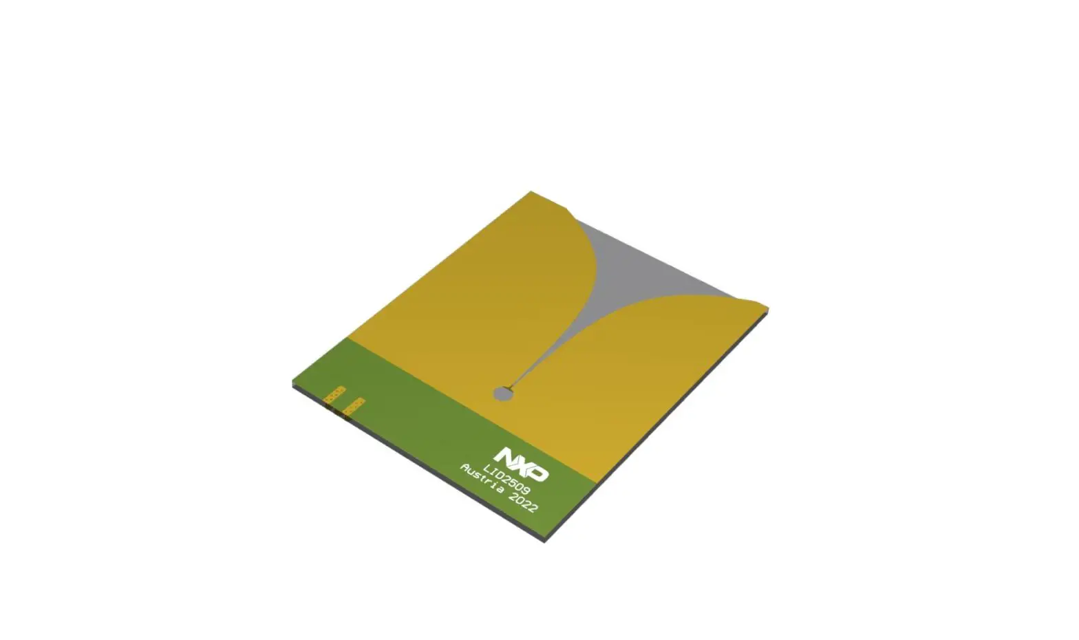
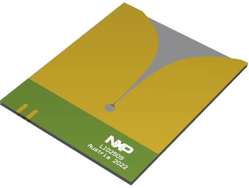
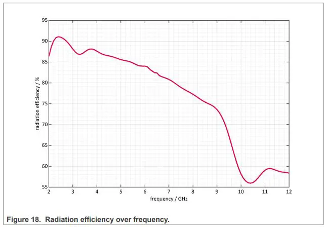
The LID2509 Vivaldi Antenna is a broadband antenna designed for ultra-wideband (UWB) and radar applications. It has a frequency range of 3.5 GHz to 9.0 GHz and a gain of 4 dBi to 7 dBi. The antenna is linearly polarized and has a horizontal polarization. Its radiation efficiency ranges from 73% to 88%. The antenna size is 77.25 mm x 63 mm x 1.8 mm and it can be used with NPG-170 or equivalent PCB laminate.
PCB Layout and Stackup
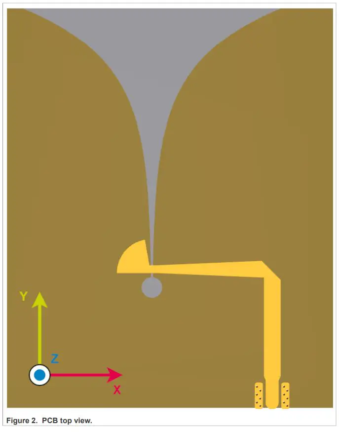
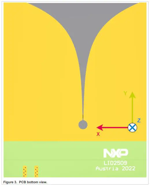
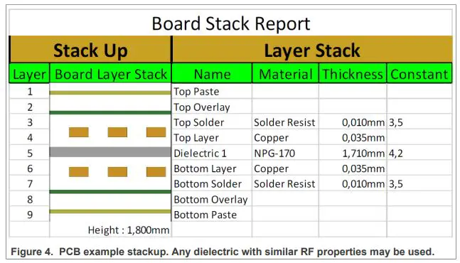
The antenna layout and stackup are shown in Figures 2, 3, and 4. Any dielectric material with similar RF properties may be used for the PCB.
Product Specifications
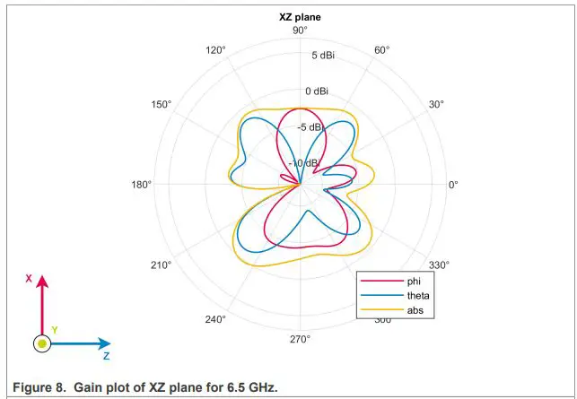
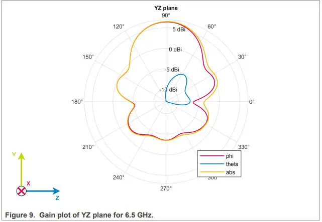
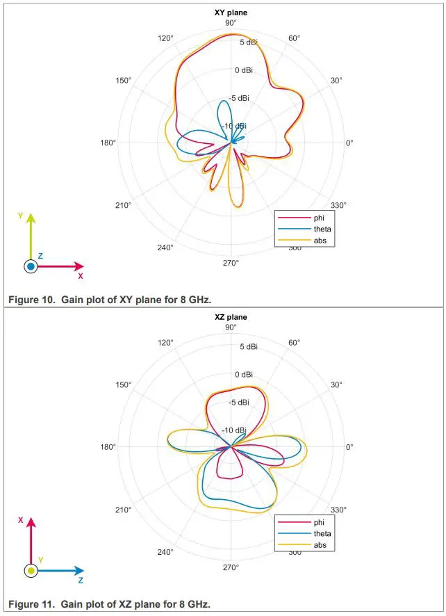
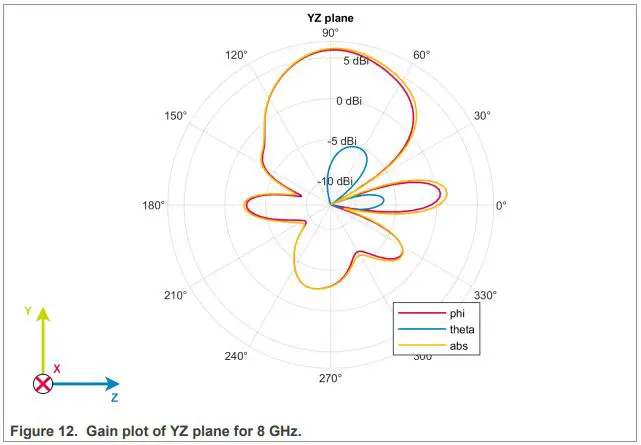
The antenna specifications are summarized in Table 1. The antenna has a VSWR of less than 1.5 and a return loss of more than 13 dB across the frequency range of 3.5 GHz to 9.0 GHz. The antenna gain varies from 4 dBi to 7 dBi depending on the frequency. The peak gain over frequency is shown in Figure 6. The gain plots of the XY, XZ, and YZ planes for frequencies of 6.5 GHz and 8 GHz are shown in Figures 7 to 11.
Product Usage Instructions
To use the LID2509 Vivaldi Antenna, follow these instructions:
- Choose a PCB laminate material with similar RF properties to NPG-170 or equivalent.
- Design the PCB layout according to the provided layout in Figures 2 and 3.
- Use the stackup shown in Figure 4 for the PCB.
- Connect the antenna to a device using an SMA Jack connector.
- Ensure that the device is compatible with the frequency range (3.5 GHz to 9.0 GHz) and polarization (horizontal) of the antenna.
- Measure the performance of the antenna to ensure that it meets the specifications provided in Table 1.
Document information
| Information | Content |
| Keywords | UWB, antenna, radar |
| Abstract | This document presents the simulation results of the LID2509 Vivaldi antenna. |
Revision history
| Rev | Date | Description |
| v.1 | 17.03.2023 | Initial version |
Introduction
The LID2509 is a linearly polarized Vivaldi antenna covering the frequency range from 3.5 GHz to 9 GHz. Therefore, it is suited to operate on most UWB channels. With a gain around 6 dBi the LID2509 is a directional antenna and was designed for UWB Radar measurements, but can also be used for UWB Ranging or any other radio technology operating in its bandwidth. The antenna features landing pads for an edge mounted SMA connector for the transition to a microstrip line. The parameters of the antenna were chosen in a way to provide a compromise between antenna size, gain and bandwidth.
The data in this user manual is derived from EM simulations only. Nevertheless, reference measurements were performed with manufactured antennas and the results match well with simulation data. Measurements showed that real antennas can have slightly reduced gain and return loss compared to simulations.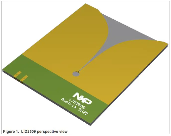
PCB Layout and Stackup
Specifications
Overview
Table 1. Antenna Parameter Overview
| Frequency | 3.5 GHz to 9.0 GHz |
| Connector Type | SMA Jack |
| VSWR | < 1.5 |
| Return Loss | > 13 dB |
| Polarization | linear, horizontal |
| Gain | 4 dBi to 7 dBi |
| Radiation Efficiency | 73% to 88% |
| Size | 77.25 mm x 63 mm x 1.8 mm |
| PCB Laminate | NPG-170 or equivalent |
Return Loss and VSWR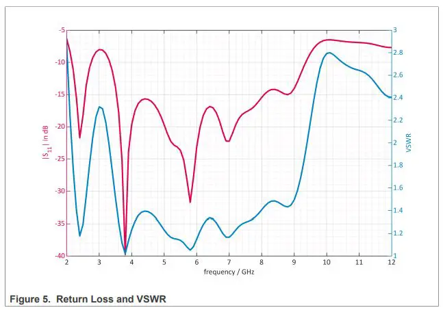
Gain
Peak Gain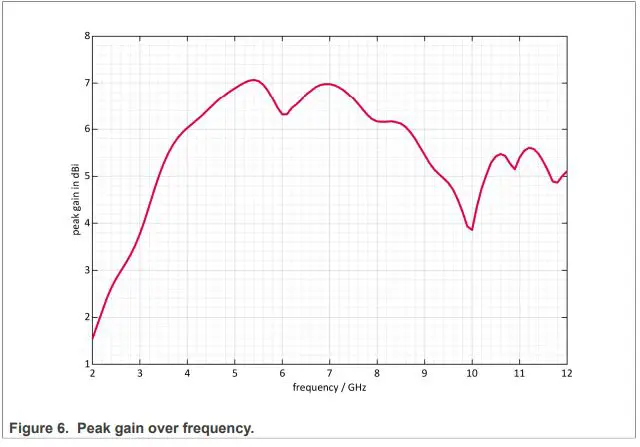
Gain Polar Plots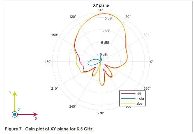
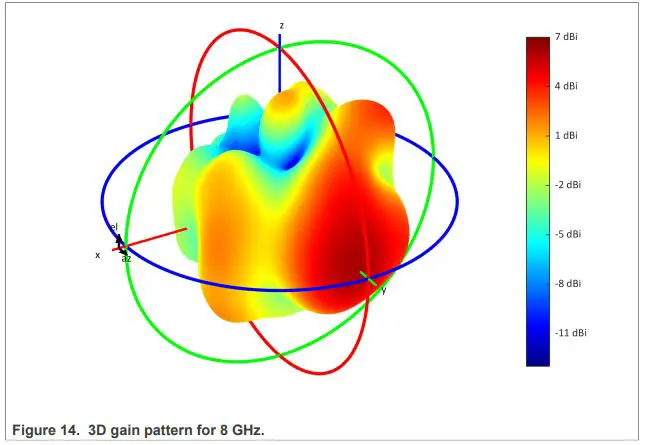
3D Gain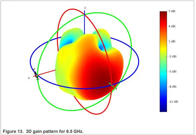
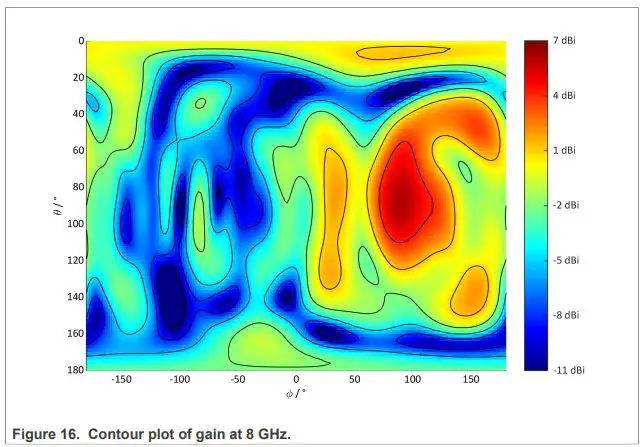
Gain Contour Plots
The spherical coordinate system used for the contour plots in this section is as in ISO 80000-2:2019. The polar angle theta starting with 0° from the Z-axis towards the XY plane and the azimuthal angle phi starting with 0° from the X-axis towards the Y-axis.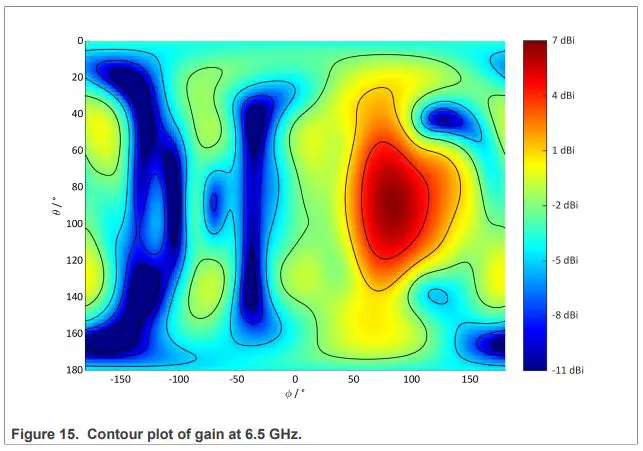
Front to Back Ratio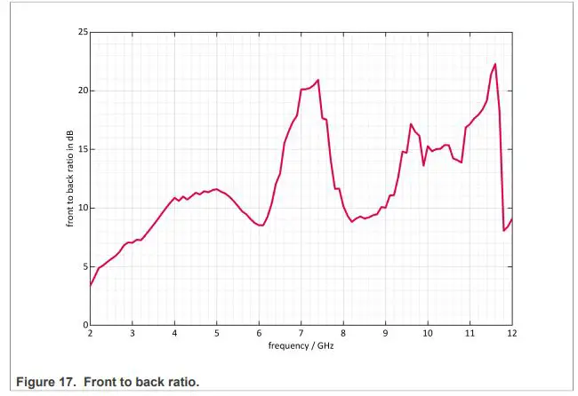
Radiation Efficiency Legal information
 Legal information
Definitions
Draft — A draft status on a document indicates that the content is still under internal review and subject to formal approval, which may result
in modifications or additions. NXP Semiconductors does not give any representations or warranties as to the accuracy or completeness of information included in a draft version of a document and shall have no liability for the consequences of use of such information.
Disclaimers
Limited warranty and liability — Information in this document is believed to be accurate and reliable. However, NXP Semiconductors does not give any representations or warranties, expressed or implied, as to the accuracy or completeness of such information and shall have no liability for the consequences of use of such information. NXP Semiconductors takes no responsibility for the content in this document if provided by an information source outside of NXP Semiconductors.
In no event shall NXP Semiconductors be liable for any indirect, incidental, punitive, special or consequential damages (including – without limitation -lost profits, lost savings, business interruption, costs related to the removal or replacement of any products or rework charges) whether or not such damages are based on tort (including negligence), warranty, breach of contract or any other legal theory.
Notwithstanding any damages that customer might incur for any reason whatsoever, NXP Semiconductors’ aggregate and cumulative liability towards customer for the products described herein shall be limited in accordance with the Terms and conditions of commercial sale of NXP Semiconductors.
Right to make changes — NXP Semiconductors reserves the right to make changes to information published in this document, including without limitation specifications and product descriptions, at any time and without notice. This document supersedes and replaces all information supplied prior to the publication hereof.
Applications — Applications that are described herein for any of these products are for illustrative purposes only. NXP Semiconductors makes no representation or warranty that such applications will be suitable for the specified use without further testing or modification.
Customers are responsible for the design and operation of their applications and products using NXP Semiconductors products, and NXP Semiconductors accepts no liability for any assistance with applications or customer product design. It is customer’s sole responsibility to determine whether the NXP Semiconductors product is suitable and fit for the customer’s applications and products planned, as well as for the planned application and use of customer’s third party customer(s). Customers should provide appropriate design and operating safeguards to minimize the risks associated with their applications and products.
NXP Semiconductors does not accept any liability related to any default, damage, costs or problem which is based on any weakness or default
in the customer’s applications or products, or the application or use by customer’s third party customer(s). Customer is responsible for doing all necessary testing for the customer’s applications and products using NXP Semiconductors products in order to avoid a default of the applications and the products or of the application or use by customer’s third party customer(s). NXP does not accept any liability in this respect.
Terms and conditions of commercial sale — NXP Semiconductors products are sold subject to the general terms and conditions of commercial sale, as published at http://www.nxp.com/profile/terms, unless otherwise agreed in a valid written individual agreement. In case an individual agreement is concluded only the terms and conditions of the respective agreement shall apply. NXP Semiconductors hereby expressly objects to applying the customer’s general terms and conditions with regard to the purchase of NXP Semiconductors products by customer.
Suitability for use in automotive applications — This NXP product has been qualified for use in automotive applications. If this product is used by customer in the development of, or for incorporation into, products or services (a) used in safety critical applications or (b) in which failure could lead to death, personal injury, or severe physical or environmental damage (such products and services hereinafter referred to as “Critical Applications”), then customer makes the ultimate design decisions regarding its products and is solely responsible for compliance with all legal, regulatory, safety, and security related requirements concerning its products, regardless of any information or support that may be provided by NXP. As such, customer assumes all risk related to use of any products in Critical Applications and NXP and its suppliers shall not be liable for any such use by customer. Accordingly, customer will indemnify and hold NXP harmless from any claims, liabilities, damages and associated costs and expenses (including attorneys’ fees) that NXP may incur related to customer’s incorporation of any product in a Critical Application.
Export control — This document as well as the item(s) described herein may be subject to export control regulations. Export might require a prior authorization from competent authorities.
Translations — A non-English (translated) version of a document, including the legal information in that document, is for reference only. The English version shall prevail in case of any discrepancy between the translated and English versions.
Security — Customer understands that all NXP products may be subject to unidentified vulnerabilities or may support established security standards or specifications with known limitations. Customer is responsible for the design and operation of its applications and products throughout their lifecycles
to reduce the effect of these vulnerabilities on customer’s applications
and products. Customer’s responsibility also extends to other open and/or proprietary technologies supported by NXP products for use in customer’s applications. NXP accepts no liability for any vulnerability. Customer should regularly check security updates from NXP and follow up appropriately.
Customer shall select products with security features that best meet rules, regulations, and standards of the intended application and make the ultimate design decisions regarding its products and is solely responsible for compliance with all legal, regulatory, and security related requirements concerning its products, regardless of any information or support that may be provided by NXP.
NXP has a Product Security Incident Response Team (PSIRT) (reachable at [email protected]) that manages the investigation, reporting, and solution release to security vulnerabilities of NXP products.
Trademarks
Notice: All referenced brands, product names, service names, and trademarks are the property of their respective owners.
NXP — wordmark and logo are trademarks of NXP B.V.
Tables
Tab. 1. Antenna Parameter Overview ……………………… 7
Please be aware that important notices concerning this document and the product(s) described herein, have been included in section ‘Legal information’
© 2023 NXP B.V.
For more information, please visit: http://www.nxp.com.


