GROM ZBee3 ZigBee Module Wireless Data Transmission Instructions
Introduction
Summary
ZBee3 is an ultra-compact, low-power, high-sensitivity 2.4 GHz IEEE 802.15.4/ ZigBee module, which can be used for wireless sensing, control and data acquisition applications.
Applications
ZBee3 module is compatible with IEEE 802.15.4/ ZigBee stack that supports a self-healing, self-organizing mesh network, while optimizing network traffic and minimizing power consumption.
The applications include but not limited to:
- Building automation & monitoring
- Environmental monitoring
- Security
- Industrial monitoring
- Automated meter reading (AMR)
Key Features
- Size: 19.3 x 13.6 x 3.0mm
- Output power: MAX 20dBm
- High RX sensitivity : -102dBm
- Outperforming link budget : 122dB
- Communication distance : SMA antenna: 800~1000m (Visual distance);
Ceramic antenna:200~300m (Visual distance) - Low power consumption
- Sleep mode : <5.0µA
- RX mode: [email protected] GHz (250 kbps O-QPSK DSSS)
- TX mode: 33.8mA@10dBm;185mA@20dBm
- Ample memory resources:
- Flash: 1024K bytes;RAM: 96K bytes
- Wide range of interfaces (both analog and digital):
- 20 x GPIO
- 12-bit 1 Msps SAR ADC
- 3 x USART transceiver
- 2 x I2C
- IEEE 802.15.4 compliant transceiver
- Optional antenna reference designs
Advantage
- Small package for small devices
- Leading link budget
- 4 PCB board, good ESD/EMC protection ability.
- Ample memory for software application
- Mesh networking capability
- ISM worldwide license-free operation
Abbreviations and Acronyms
ADC Analog-to -Digital Converter
API Application Programming Interface
DC Direct Current
DTR Data Terminal Ready
DIP Duap In-line package
EEPROM Electrically Erasable Programmable Read-Only Memory
ESD Electrostatic Discharge
GPIO General Purpose Input/Output
HAL Hardware Abstraction Layer
HVAC Heating, Ventilating and Air Conditioning
HW Hardware
TWI Inter-Integrated Circuit
IEEE Institute of Electrical and Electrionics Engineers
IRQ Interrupt Request
ISM Industrial, Scientific and Medical radio band
JTAG Digital interface for debugging of embedded device, also known as IEEE
1149.1 standard interface
MAC Medium Access Control layer
MCU Microcontroller Unit. In this document it also means the processor, which is the core of ZigBee module
NWK Network layer
OEM Original Equipment Manufacturer
OTA Over-The-Air upgrade
PCB Printed Circuit Board
PER Package Error Ratio
PHY Physical layer
RAM Random Access Memory
RF Radio Frequency
RTS/CTS Request to Send/ Clear to Send
RX Receiver
SMA Surface Mount Assembly
SPI Serial Peripheral Interface
SW Software
TX Transmitter
UART Universal Asynchronous Receiver/Transmitter
USART Universal Synchronous/Asynchronous Receiver/Transmitter
USB Universal Serial Bus
ZigBeePRO Wireless networking standards targeted at low-power applications
802.15.4 The IEEE 802.15.4-2003 standard applicable to low-rate wireless PAN
- IEEE Std 802.15.4-2003 IEEE Standard for Information technology – Part 15.4 Wireless Medium Access Control (MAC) and Physical Layer (PHY) Specifications for Low-Rate Wireless Personal Area Networks (LR-WPANs)
- ZigBee Specification. ZigBee Document 053474r17, October 19, 2007
Specifications
Electrical Characteristics
Absolute Maximum Ratings
Table 2-1. Absolute Maximum Ratings
| Parameters | Min | Max |
| Power supply range(VCC) | 1.75V | 3.8V |
| Pin working voltage range(exclude ADC pin) | -0.3V | VDD_PADS+0.3 |
| Max driving current of all I/O | 200 mA | |
| Max RX RF level | +10 dBm |
Note:
Absolute Maximum Ratings are the values beyond which damage to the module may occur. Under no circumstances must the absolute maximum ratings given in this table be violated. Stresses beyond those listed under “Absolute Maximum Ratings” may cause permanent damage to the module.
Test Conditions
Table 2-2. Test conditions (unless otherwise stated), VCC = 3.3V, Tamp = 25°C
| Parameters | Range | Unit |
| TX current (@20dBm) | 200 | mA |
| RX current | 9.4 | mA |
| Sleeping current | <5.0 | μA |
RF Characteristics
Table 2-3. RF Characteristics
| Parameters | Test Conditions | Range | Unit |
| Frequency Band | 2400~2483.5 | MHz | |
| Numbers of Channels | 16 | ||
| Channel Interval | 5 | MHz | |
| Transmitter Output Power | -20 to +20 | dBm | |
| Receive Sensitivity (90%) | -104 | dBm | |
| Max data transmit speed | 250 | kbps | |
| TX Output/ RX Input Nominal Impedance | 50 | Ω | |
Microcontroller Characteristics
Table 2-4. Microcontroller Characteristics
| Parameters | Test Conditions | Range | Unit |
| On-chip Flash Memory size | 512K~1024K | bytes | |
| On-chip RAM size | 64K~96K | bytes | |
| Operation Frequency | 80 | MHz |
Module Interfaces characteristics
Table 2-5. Module Interfaces characteristics
| Parameters | Test Conditions | Range | Unit |
| UART Maximum Baud Rate | 230400 | bps | |
| Analog input impedance | >1 | MΩ | |
| Analog input current | 0 – VREF | V | |
| I2C Maximum Clock | 1 | MHz | |
| Real Time Oscillator Frequency | 32.768 | KHz |
Physical/Environmental Characteristics
Table 2-6. Physical/Environmental Characteristics
| Parameter | Value | Remark |
| Size (L*W*H) | 19.3×13.6×3.0mm | |
| Working temp. | -40°C to +85°C | |
| Operating Relative Humidity Range | <= 95%RH |
Pin Configuration
Picture 2-1. Size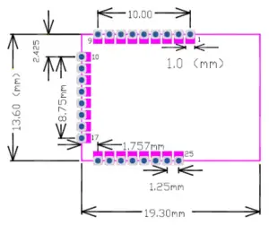
Picture 2-1: Size (mm)
Picture 2-2. Pin Configuration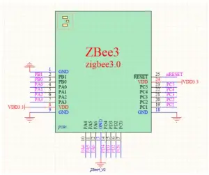
Table 2-7. Pin instruction
| Module Pin No. | Pin No. | Signal | Directio n | Description |
| 1 | GND | – | Ground | |
| 2 | 15 | PB01 | I/O | Digital I/O |
| EM4WU3 | I | |||
| 3 | 16 | PB00 | I/O | Digital I/O |
| 4 | 17 | PA00 | I/O | Digital I/O |
| 5 | 18 | PA01 | I/O | Digital I/O |
| SWCLK | I | |||
| 6 | 19 | PA02 | I/O | Digital I/O |
| SWDIO | I/O | |||
|
7 |
20 | PA03 | I/O | Digital I/O |
| SWV | O | |||
| TDO | O | |||
| TRACEDATA 0 | ||||
| 8 | 3.3V | – | DC supply,1.8~3.6V | |
| 9 | GND | – | Ground | |
| 10 | 21 | PA04 | I/O | Digital I/O |
| TDI | ||||
| TRACECLK | ||||
| 11 | 22 | PA05 | I/O | Digital I/O |
| EM4WU0 | ||||
| 12 | 23 | PA06 | I/O | Digital I/O |
| 13 | GND | – | Ground | |
| 14 | 28 | PD04 | I/O | Digital I/O |
| 15 | 29 | PD03 | I/O | Digital I/O |
| 16 | 30 | PD02 | I/O | Digital I/O |
| EM4WU9 | I | |||
| 17 | 1 | PC00 | I/O | Digital I/O |
| 18 | GND | – | Ground | |
| 19 | 2 | PC01 | I/O | Digital I/O |
| 20 | 3 | PC02 | I/O | Digital I/O |
| 21 | 4 | PC03 | I/O | Digital I/O |
| 22 | 5 | PC04 | I/O | Digital I/O |
| 23 | 6 | PC05 | I/O | Digital I/O |
| EM4WU7 | I | |||
| 24 | 3.3V | – | DC supply,1.8~3.6V | |
| 25 | 9 | RESETn | I | Reset Pin |
Antenna Specifications
Use U.FL to connect external antenna:
Picture 2-3. U.FL connector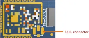
Integrated ceramic antenna:
Picture 2-4. Ceramic antenna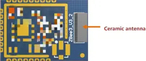
Attention when using ceramic antenna:
- Please avoid installing the module in a complete metal enclosure.
- Please avoid placing high profile components/metal next to antenna (1 cm at least, suggest more than 2.7 cm).
- ZigBee module should not be placed next to consumer electronics which might interfere with ZigBee’s RF frequency band, like transformer.
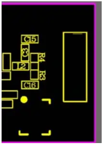
User should try to avoid other components or line interfere ceramic antenna when designing board:
- Wires or other components avoid surrounding ceramic antenna
- Ceramic antenna should be extended to the board
- Don’t use metal shell to cover the PCB antenna
Picture 2-4. Components Location
******Soldering way for convert ceramic antenna to U.FL:
U.FL soldering way:C3=2.7nh, R4=NC, R3=2.7pF, C16=2.7nh
Ordering Information
Product Type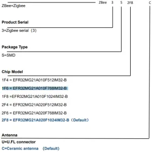
Contact Us
Hangzhou Grom Technology Co.,Ltd.
Add: Room800, Building3#, Longtan Rd 16#, Cangqian street, Yuhang District, Hangzhou,
Zhejiang Province, China. 311121
Tel:+86-571-88695993
Email: [email protected]
Website:www.gromiot.com
FCC Statement
FCC standards: FCC CFR Title 47 Part 15 Subpart C Section 15.247
Chip antenna with Antenna gain 2dBi Integral antenna(SMA antenna connector)with Antenna gain 2dBi
This device complies with part 15 of the FCC Rules. Operation is subject to the following two conditions: (1) This device may not cause harmful interference, and (2) this device must accept any interference received, including interference that may cause undesired operation.
Any Changes or modifications not expressly approved by the party responsible for compliance could void the user’s authority to operate the equipment.
Note: This equipment has been tested and found to comply with the limits for a Class B digital device, pursuant to part 15 of the FCC Rules. These limits are designed to provide reasonable protection against harmful interference in a residential installation. This equipment generates, uses and can radiate radio frequency energy and, if not installed and used in accordance with the instructions, may cause harmful interference to radio communications.
However, there is no guarantee that interference will not occur in a particular installation. If this equipment does cause harmful interference to radio or television reception, which can be determined by turning the equipment off and on, the user is encouraged to try to correct the interference by one or more of the following measures:
- Reorient or relocate the receiving antenna.
- Increase the separation between the equipment and receiver.
- Connect the equipment into an outlet on a circuit different from that to which the receiver is connected.
- Consult the dealer or an experienced radio/TV technician for help.
FCC Radiation Exposure Statement
The modular can be installed or integrated in mobile or fix devices only. This modular cannot be installed in any portable device without further certificate (such as C2CP with SAR). This modular complies with FCC RF radiation exposure limits set forth for an uncontrolled environment. This transmitter must not be co-located or operating in conjunction with any other antenna or transmitter. This modular must be installed and operated with a minimum distance of 20 cm between the radiator and user body.
If the FCC identification number is not visible when the module is installed inside another device, then the outside of the device into which the module is installed must also display a label referring to the enclosed module. This exterior label can use wording such as the following: “Contains Transmitter Module FCC ID: 2AZEG- ZBEE3S2F8C Or Contains FCC ID: 2AZEG-ZBEE3S2F8C ”
When the module is installed inside another device, the user manual of the host must contain below warning statements;
This device complies with Part 15 of the FCC Rules. Operation is subject to the following two conditions:
(1) This device may not cause harmful interference;
(2) This device must accept any interference received, including interference that may cause undesired operation.
Note: This equipment has been tested and found to comply with the limits for a Class B digital device, pursuant to part 15 of the FCC Rules. These limits are designed to provide reasonable protection against harmful interference in a residential installation. This equipment generates, uses and can radiate radio frequency energy and, if not installed and used in accordance with the instructions, may cause harmful interference to radio communications.
However, there is no guarantee that interference will not occur in a particular installation. If this equipment does cause harmful interference to radio or television reception, which can be determined by turning the equipment off and on, the user is encouraged to try to correct the interference by one or more of the following measures:
- Reorient or relocate the receiving antenna.
- Increase the separation between the equipment and receiver.
- Connect the equipment into an outlet on a circuit different from that to which the receiver is connected.
- Consult the dealer or an experienced radio/TV technician for help.
Changes or modifications not expressly approved by the party responsible for compliance could void the user’s authority to operate the equipment.
The devices must be installed and used in strict accordance with the manufacturer’s instructions as described in the user documentation that comes with the product.
Any company of the host device which install this modular with modular approval should perform the test of radiated & conducted emission and spurious emission, etc. according to FCC part 15C : 15.247 and 15.209 & 15.207 ,15B Class B requirement, Only if the test result comply with FCC part 15C : 15.247 and 15.209 & 15.207 ,15B Class B requirement, then the host can be sold legally
Add: Room800,Building3#,Longtan Rd 16#,Cangqian street, Hangzhou City, China. 311121
Website:www.gromiot.com
![]()


