WNC IMA2 Tape and Reel Module
Packing lnformation(TBD)
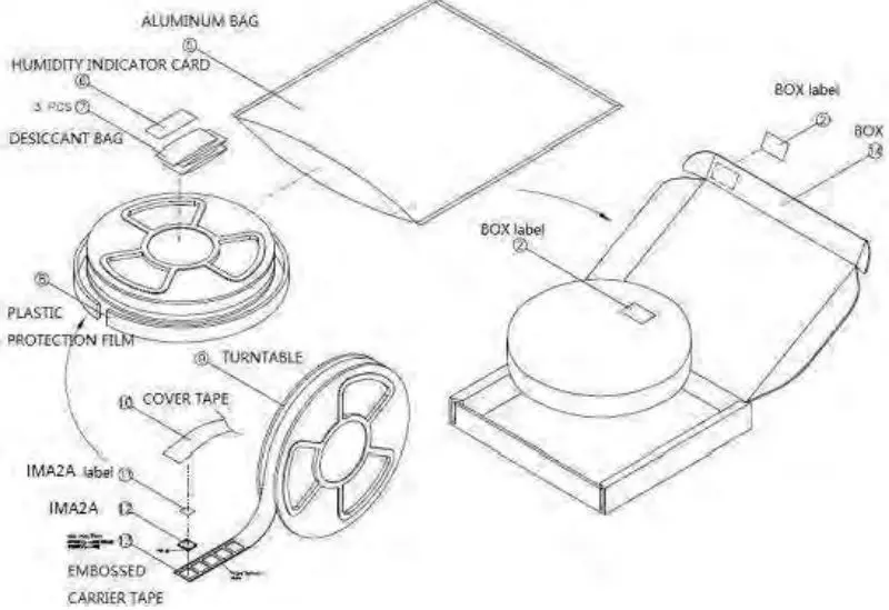
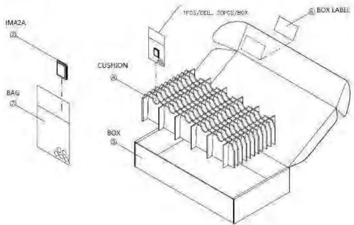
Tape-and-Reel Package
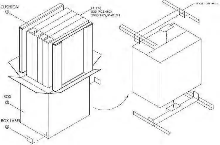
The module is delivered in tape-and-reel packaging based on MPQ (500 pcs./reel; 4 reels/carton).
Single Packaging for Samples
Samples are packaged at 50 pcs./box. There is no vacuum packaging. Samples must be baked for 8 hours at 85 °C before SMT.
MSL level
The IMA2 module MSL level is 3.
Design Guide
Power Trace Design
Power trace layout suggestion: At least 22 µF, 0.1 µF, and 100 pF capacitors are required; place the capacitors as close to the power pins as possible. Power trace should possess sufficient line width to withstand its respective current listed in the table below.
| Net Name | Peak Current Value for PCB Power Trace Design |
| Power (37-42) total | 1A |
| VREF | S0mA |
| UIM_VCC | 30mA |
Table 6-1. Reference current for power trace
Please select the DCDC that can satisfy the output (1 A) as the power supply of the module.
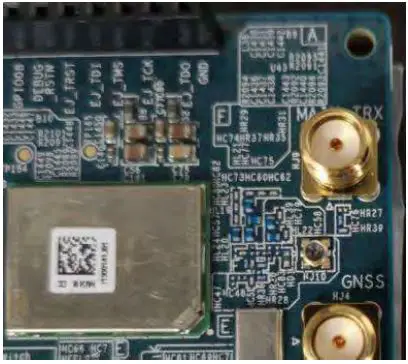
RF Pad Design
We recommend that a ground not be present under the surface of the RF pads in the layout. Details are included below. Layer 2 has the same exclusion area as Layer 1.
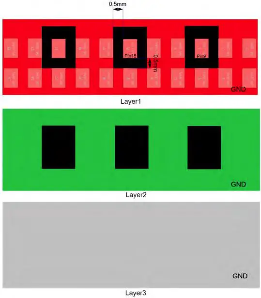
Figure 6-1. Sample RF pad layout
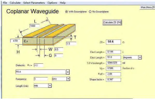
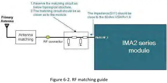
The RF trace between RF pads and antenna should as shorter as possible with 50ohrn characteristic impedance.
The characteristic impedance depends on the dielectric of PCB, the track width and the
ground plane spacing. Coplanar Waveguide type is required. The detail simulation as below.
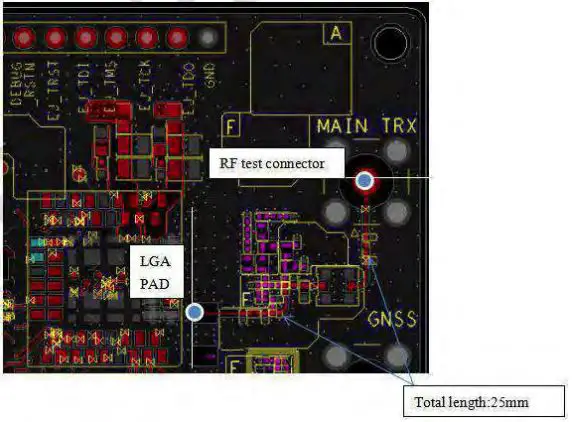
The RF trace of the test board which was used in the FCC test is defined as below.
RF Matching Guide
Mounting Considerations(TBD)
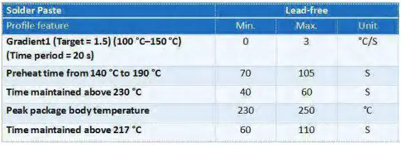
This section details the recommended reflow profile when the module is mounted onto other boards.
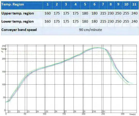
Process limit
PCB Pad Design
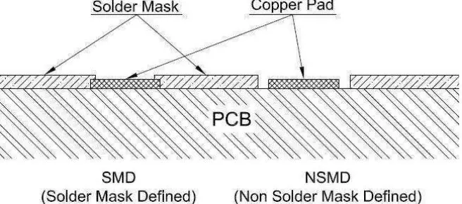
We recommend a non-solder mask with defined (NSMD) type for the solder pads of the PCB on which IMA2 modules will be mounted. This type of design enables high soldering reliability during the SMT process.
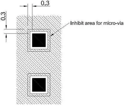
We recommend not placing via or micro-via that is not covered by solder resistance within 0.3 mm around the pads unless it carries the same signal of the pad itself. Refer to the following figure.
Only blind holes are allowed in the pad. Through holes are not allowed.
LTE Power Saving Mode
Note: Details will be provided in a future revision of this document.
Safety Recommendations
Be sure use of this product is allowed in the country and in the environment required. Use of this product may be dangerous and must be avoided in the following areas:
- Where it may interfere with other electronic devices in environments such as hospitals, airports, and aircraft
- Where there is a risk of explosion such as gasoline stations and oil refineries
- The user is responsible for compliance with the legal and environmental regulations of their location of use.
- Do not disassemble the product; any evidence of tampering will compromise the warranty’s validity.
- We recommend following the instructions of the hardware user guides for a correct wiring of the product. The product must be supplied with a stabilized voltage source, and the wiring must conform to relevant security and fire-prevention regulations.
- This product must be handled with care; avoid any contact with the pins because electrostatic discharge may damage the product. Exercise the same level of caution regarding the UIM card; carefully check the instructions for its use. Do not insert or remove the UIM when the product is in power-saving mode.
- The system integrator is responsible for the functioning of the final product; therefore, care must be taken for the external components of the module as well as for project or installation issues-there may be a risk of disturbing the GSM network or external devices or of impacting device security. If you have any questions, refer to the technical documentation and the relevant regulations in force.
- Every module must be equipped with a proper antenna with specific characteristics. The antenna must be installed with care in order to avoid any interference with other electronic devices.
initialisms
initialisms and Definitions
| lnitialism | Definition |
| AC | Alternating current |
| DC | Direct current |
| ETSI | European Telecommunications Standards Institute |
| GND | Ground |
| GPIO | General purpose input output |
| 1/0 | Input/output |
| loT | Internet of Things |
| 12C | Inter-integrated circuit |
| LGA | Land grid array |
| LTE | Long Term Evolution |
| N/A | Not/applicable |
| OS | Operating system |
| PIN | Personal identification number |
| SIM | Subscriber identity module |
| SPI | Serial peripheral interface |
| UART | Universal asynchronous receiver-transmitter |
| UIM | User identity module |
| USB | Universal serial bus |
| Vref | Voltage reference |
| RFU | Reserved for future use |
| HD-FDD | Half Duplex-FDD |
| WNC | Wistron NeWeb Corporation |


