ALINX FL 1010 FMC 2 40-Pin Expansion Module
FL1010 Module General Description
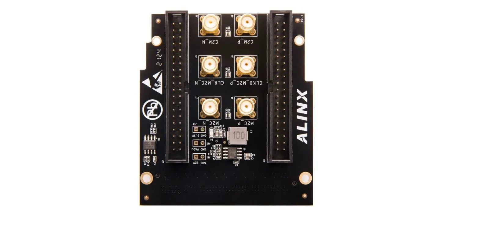
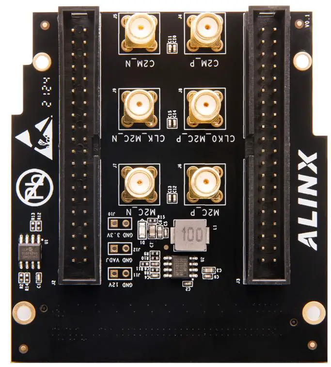
ALINX FMC to 2*40-Pin Expansion ports module FL1010 is to solve the problem of users expanding the pin-type IO port on the FMC connector, which is convenient for users to use DuPont cable or flat cable to connect to external devices. The FL1010 board expands with 2 40-pin standard interfaces, a total of 68 user IOs; and 6 SMA interfaces for connecting FMC transceivers. The FMC interface of FL1010 is a standard LPC interface, used to connect to the FPGA development board, and meets the VITA57.1 standard. The connector model of FMC is ASP_134604_01. The FL1010 module is as follows:
Part 1.1: FL1010 Module Detail Parameter
FL1010 module detail parameters are listed below:
- LPC Connectors
- 2*40-Pin Expansion Ports
- 6 SMAs, 1 DP transmission, 1 DP receiving
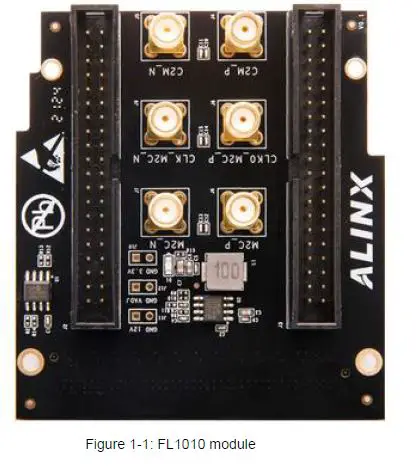
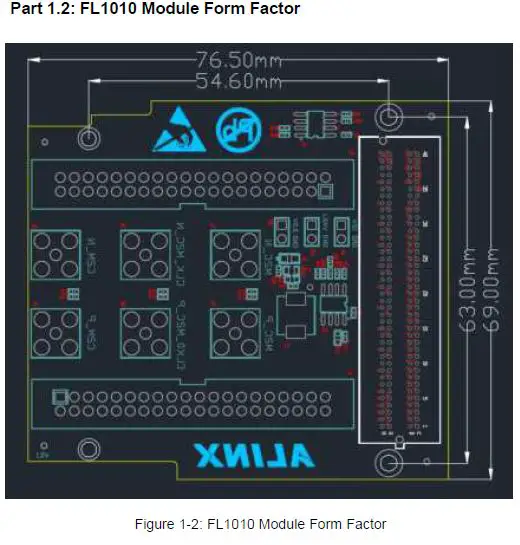
Part 1.2: FL1010 Module Form Factor
FL1010 Module Function Description
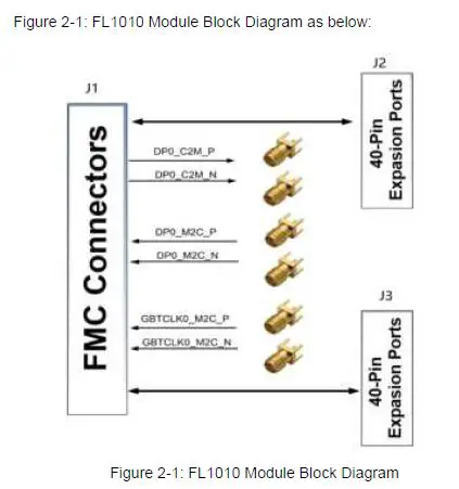
Part 2.1: FL1010 Module Block Diagram
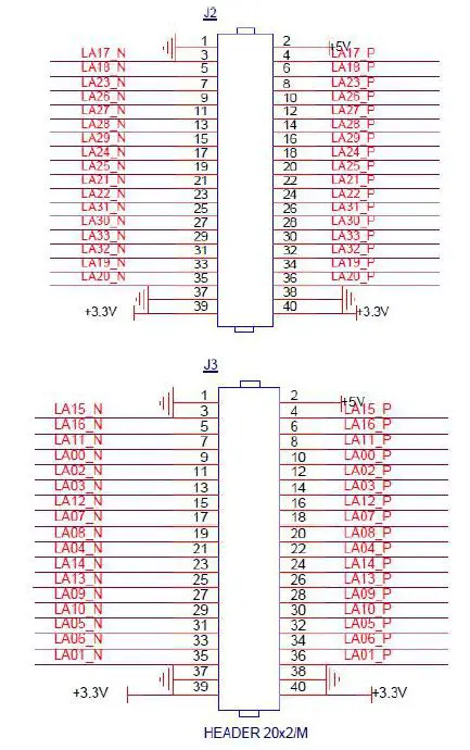
Part 2.2: FMC LPC Module Pin Assignment
Only the power and interface signals are listed below, and the GND signal is not listed. Users can refer to the schematic diagram.
| FMC Pin Number | Network Name | Description |
| G2 | CLK1_M2C_P | Not Used |
| G3 | CLK1_M2C_N | Not Used |
| G6 | LA00_P | PIN10 of J3 |
| G7 | LA00_N | PIN 9 of J3 |
| G9 | LA03_P | PIN 14 of J3 |
| G10 | LA03_N | PIN 13 of J3 |
| G12 | LA08_P | PIN 20 of J3 |
| G13 | LA08_N | PIN 19 of J3 |
| G15 | LA12_P | PIN 16 of J3 | ||
| G16 | LA12_N | PIN 15 of J3 | ||
| G18 | LA16_P | PIN 6 of J3 | ||
| G19 | LA16_N | PIN 5 of J3 | ||
| G21 | LA20_P | PIN 36 of J2 | ||
| G22 | LA20_N | PIN 35 of J2 | ||
| G24 | LA22_P | PIN 24 of J2 | ||
| G25 | LA22_N | PIN 23 of J2 | ||
| G27 | LA25_P | PIN 20 of J2 | ||
| G28 | LA25_N | PIN 19 of J2 | ||
| G30 | LA29_P | PIN 16 of J2 | ||
| G31 | LA29_N | PIN 15 of J2 | ||
| G33 | LA31_P | PIN 26 of J2 | ||
| G34 | LA31_N | PIN 25 of J2 | ||
| G36 | LA33_P | PIN 30 of J2 | ||
| G37 | LA33_N | PIN 29 of J2 | ||
| G39 | VADJ | VADJ Power Supply | ||
| H4 | CLK0_M2C_P | |||
| H5 | CLK0_M2C_N | |||
| H7 | LA02_P | PIN 12 of J3 | ||
| H8 | LA02_N | PIN 11 of J3 | ||
| H10 | LA04_P | PIN 22 of J3 | ||
| H11 | LA04_N | PIN 21 of J3 | ||
| H13 | LA07_P | PIN 18 of J3 | ||
| H14 | LA07_N | PIN 17 of J3 | ||
| H16 | LA11_P | PIN 8 of J3 | ||
| H17 | LA11_N | PIN 7 of J3 | ||
| H19 | LA15_P | PIN 4 of J3 | ||
| H20 | LA15_N | PIN 3 of J3 | ||
| H22 | LA19_P | PIN 34 of J2 | ||
| H23 | LA19_N | PIN 33 of J2 | ||
| H25 | LA21_P | PIN 22 of J2 | ||
| H26 | LA21_N | PIN 21 of J2 | ||
| H28 | LA24_P | PIN 18 of J2 | ||
| H29 | LA24_N | PIN 17 of J2 | ||
| H31 | LA28_P | PIN 14 of J2 | ||
| H32 | LA28_N | PIN 13 of J2 | ||
| H34 | LA30_P | PIN 28 of J2 | ||
| H35 | LA30_N | PIN 27 of J2 | ||
| H37 | LA32_P | PIN 32 of J2 | ||
| H38 | LA32_N | PIN 31 of J2 | ||
| H40 | VADJ | VADJ Power Supply | ||
| C2 | DP0_C2M_P | SMA Connector J4 | ||
| C3 | DP0_C2M_N | SMA Connector J5 | ||
| C6 | DP0_M2C_P | SMA Connector J6 | ||
| C7 | DP0_M2C_N | SMA Connector J7 | ||
| C10 | LA06_P | PIN 34 of J3 | ||
| C11 | LA06_N | PIN 33 of J3 | ||
| C14 | LA10_P | PIN 30 of J3 | ||
| C15 | LA10_N | PIN 29 of J3 |
| C18 | LA14_P | PIN 24 of J3 |
| C19 | LA14_N | PIN 23 of J3 |
| C22 | LA18_P | PIN 6 of J2 |
| C23 | LA18_N | PIN 5 of J2 |
| C26 | LA27_P | PIN 12 of J2 |
| C27 | LA27_N | PIN 11 of J2 |
| C30 | SCL | EEPROM Clock |
| C31 | SDA | EEPROM Data |
| C34 | GA0 | Low Bit of EEPROM Address |
| C35 | +12V | +12V Power Supply |
| C37 | +12V | +12V Power Supply |
| D4 | GBTCLK0_M2C_P | SMA Connector J8 |
| D5 | GBTCLK0_M2C_N | SMA Connector J9 |
| D8 | LA01_P | PIN 36 of J3 |
| D9 | LA01_N | PIN 35 of J3 |
| D11 | LA05_P | PIN 32 of J3 |
| D12 | LA05_N | PIN 31 of J3 |
| D14 | LA09_P | PIN 28 of J3 |
| D15 | LA09_N | PIN 27 of J3 |
| D17 | LA13_P | PIN 26 of J3 |
| D18 | LA13_N | PIN 25 of J3 |
| D20 | LA17_P | PIN 4 of J2 |
| D21 | LA17_N | PIN 3 of J2 |
| D23 | LA23_P | PIN 8 of J2 |
| D24 | LA23_N | PIN 7 of J2 |
| D26 | LA26_P | PIN 10 of J2 |
| D27 | LA26_N | PIN 9 of J2 |
| D32 | +3.3V | +3.3V Power Supply |
| D35 | GA1 | The Second Bit of EEPROM Address |
Part 2.3: 40-Pin Expansion Ports
The pin definition of the 40-pin header is the same as that of the ALINX FPGA development board. PIN1, PIN37, and PIN38 are GND, PIN2 is +5V, and PIN39 and PIN40 are 3.3V; Others are IO ports and the level standard of IO ports is determined by the FPGA development board.