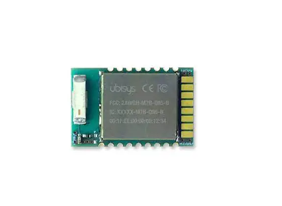
ubisys M7B-Q95 Zigbee Luminaire Module
OVERVIEW
The ubisys wireless connectivity module series M7B-Q95-B -power wireless system on chip, which comprises an ARM Cortex-M4, 512KB flash ROM, 64 KB SRAM and a multi-channel, multi-protocol radio with quasi-concurrent support for IEEE 802.15.4 (zigbee, rf4ce, Thread) and Bluetooth Low Energy (BLE). Additional flash memory is available on the module to store over-the-air upgrade images or other data.
The-loaded applications, which greatly simplify the design and manufacturing of connected products. For example, ready-to-use applications for typical lighting control applications are available, which can directly steer power stages using PW M signals or analogue control circuits using 0-10V signals. In addition, customized firmware can be ordered, which allows interfacing to existing digital control circuits using proprietary protocols running over UART, SPI or I²C.
These modules are the perfect choice for manufacturers who want to produce standards-compliant products in order to take advantage of direct device-to-device communications within Zigbee mesh networks. This creates opportunities with established eco-systems like Philips hue, IKEA Trådfri, amazon Echo with integrated Zigbee Hub, OSRAM Lightify, and, of course, ubisys Smart Home, as well as other platforms based on Zigbee technology.
You have decided for a high-quality product with first-rate support!
This hardware reference manual provides information for engineers involved in the integration of this module into a product. Separate documentation is available for applications, which come preinstalled on the modules.
If you have any questions or need additional support, please visit the engineering support pages at http://www.ubisys.de/en/engineering/support.html for contact details.
FEATURES
- Designed in Germany using high-quality, enduring parts for many years of life expectancy
- MCU: Advanced 32-bit ARM Cortex-M4 running at 32MHz with 64KB SRAM and 512KB flash ROM
- PHY: 10dBm transmit power,
- 98dBm receiver sensitivity
- Integrated chip antenna
- Low power dissipation
- Multi-channel, multi-mode transceiver
- Pre-loaded firmware, for instance dimmable light with switch input for local control
- Customizations available
M7B-Q95-B4 (Form Factor B, Pinout Scheme # 4)
Status: Active. Recommended for new designs
The following signals are available: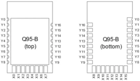
The following signals are available:
| Module Pin | Function | Description |
| Y0 | GND | Ground |
| Y1/X7 | GPIO23 ANIO2 | Analog input, general purpose digital I/O,peripheral I/O for UART2:TX, SPIM:MISO, SPIS:MOSI, I2CM:SDA, I2CS:SDA, I2SM:SDI, PWM2, TS2, LED0 |
| Y2/X6 | GPIO26 ANIO5 | Analog input, general purpose digital I/O,peripheral I/O for UART1:TX, SPIM:MOSI, SPIS:MISO, I2CM:SCL, I2CS:SCL, I2SM:SDO, PWM5, LED3,PROG_EN |
| Y3/X5 | GPIO25 ANIO4 | Analog input, general purpose digital I/O,peripheral I/O for UART1:RX, UART2:TX, SPIM:SCLK, SPIS:SSN, I2CM:SDA, I2CS:SDA, I2SM:SCK, PWM4, TS2, LED2 |
| Y4/X4 | GPIO24 ANIO3 | Analog input, general purpose digital I/O,peripheral I/O for UART2:RX, SPIM:SSN, SPIS:SCLK, I2CM:SCL, I2CS:SCL, I2SM:WS, PWM3, TS3, LED1 |
| Y5/X3 | VDD | Power supply, 3.3V |
| Y6/X2 | GPIO7 | General purpose digital I/O,peripheral I/O for SPIS:SCLK, I2CM: SCL, I2CS:SCL, PWM5, LED1, JTAG:TCK, SWD:CLK |
| Y7/X1 | RESET | Reset line (active-low) |
| Y8/X0 | GND | Ground |
| Y9/X8 | GPIO6 | General purpose digital I/O,peripheral I/O for SPIM:MOSI, SPIS:SSN, I2SM:SDO, PWM4, JTAG:TMS, SWD:I/O |
| Y10/X9 | GPIO8 | General purpose digital I/O,peripheral I/O for UART1:TX, SPIS:MOSI, I2CM:SDA, I2CS:SDA, PWM4, LED2, JTAG:TDI |
| Y11/X10 | GPIO2 | General purpose digital I/O,peripheral I/O for UART2:TX, SPIM:SCLK, SPIS:MOSI, I2CM:SDA, I2CS:SDA, I2SM:SCK, PWM2, TS2, LED2 |
| Y12/X11 | GPIO3 | General purpose digital I/O, peripheral I/O for UART2:RX, SPIM:MOSI, SPIS:SCLK, I2CM:SCL, I2CS:SCL, I2SM:SDO, PWM3, TS3, LED3 |
| Y13/X12 | GPIO9 | General purpose digital I/O,peripheral I/O for UART1:RX, SPIS:MISO, PWM5, LED3, JTAG:TDO, SWD:V |
| Y14/X13 | GPIO10 | General purpose digital I/O, peripheral I/O for CLKOUT, UART1:TX, SPIS:SSN, PWM0, TS0, LED0 |
| Y15/X14 | GPIO11 | General purpose digital I/O,peripheral I/O for UART1:RX, UART2:RX, SPIS:SCLK, PWM1, TS1, LED1 |
| Y16/X15 | GPIO5 | General purpose digital I/O,peripheral I/O for SPIM:MOSI, SPIS:SSN, I2SM:SDO, PWM4 |
This results in the following mapping of often used peripheral I/Os (LED, PW M, UART1, UART2, SPI master/slave, I²C master/slave) and analogue inputs, together with resulting wake-up and interrupt request capabilities
| Module | GPIO | ANIO | Port | IRQ1 | Wake-up | LED | PWM | UART1 | UART2 | SPI | I2C | SPI | I2C |
| Pin Master Slave | |||||||||||||
| Y1/X7 | 23 | 2 | C | 4 | Y | 0 | 2 | – | TX | MISO | SDA | MOSI | SDA |
| Y2/X6 | 26 | 5 | C | 7 | Y | 3 | 5 | TX | – | MOSI | SCL | MISO | SCL |
| Y3/X5 | 25 | 4 | C | 6 | Y | 2 | 4 | RX | TX | SCLK | SDA | SSN | SDA |
| Y4/X4 | 24 | 3 | C | 5 | Y | 1 | 3 | – | RX | SSN | SCL | SCLK | SCL |
| Y6/X2 | 7 | – | A | 7 | Y | 1 | 5 | – | – | – | SCL | SCLK | SCL |
| Y9/X8 | 6 | – | A | 6 | Y | – | 4 | – | – | MOSI | – | SSN | – |
| Y10/X9 | 8 | – | B | 0 | Y | 2 | 4 | TX | – | – | SDA | MOSI | SDA |
| Y11/X10 | 2 | – | A | 2 | Y | 2 | 2 | – | TX | SCLK | SDA | MOSI | SDA |
| Y12/X11 | 3 | – | A | 3 | Y | 3 | 3 | – | RX | MOSI | SCL | SCLK | SCL |
| Y13/X12 | 9 | – | B | 1 | Y | 3 | 5 | RX | – | – | SCL | MISO | – |
| Y14/X13 | 10 | – | B | 2 | Y | 0 | 0 | TX | – | – | – | SSN | – |
| Y15/X14 | 11 | – | B | 3 | Y | 1 | 1 | RX | RX | – | – | SCLK | – |
| Y16/X15 | 5 | – | A | 5 | Y | – | 4 | – | – | MOSI | – | SSN | – |
These special purpose debugging and firmware programming signals need to be handled with care. Specifically, the application circuit must be designed in a way that does not start the processor in programming/debugging mode. If in-application debugging is desired, avoid using any of the signals below and route them to a suitable probe connector.
| Module Pin | GPIO | SWD | JTAG | Remarks |
| Y2/X6 | 26 | PROG_EN | PROG_EN | Low for about one second, then high enables programming mode for 32 seconds. CAUTION: Make sure that the host board does not inadvertently generate such a condition! |
| Y6/X2 | 7 | SWDCLK | TCK | |
| Y7/X1 | – | – | – | Active-low system reset |
| Y9/X8 | 6 | SWDIO | TMS | |
| Y10/X9 | 8 | – | TDI | |
| Y13/X12 | 9 | SWDV | TDO |
1Note: It is possible to select one port per IRQ line. Multiple GPIOs can be configured to raise an interrupt as long as they belong to different IRQ lines.n
Light Firmware Pin Assignments
Software uses the following mapping of functions to module pins:
| Module Pin | Function | Type | Description |
| Y0 | GND | G | Ground |
| Y1/X7 | GPIO23 | D/O | Light Output #3 |
| Y2/X6 | GPIO26 | A/I | Voltage Monitoring for Over-Voltage Protection |
| Y3/X5 | GPIO25 | A/I | Temperature Monitoring for Over-Temperature Protection |
| Y4/X4 | GPIO24 | A/I | Current Monitoring for Over-Current Protection |
| Y5/X3 | VDD | P | Power supply, 3.3V |
| Y6/X2 | GPIO7 | – | Currently not used |
| Y7/X1 | RESET | D/I | Reset line (active-low) |
| Y8/X0 | GND | G | Ground |
| Y9/X8 | GPIO6 | D/I | Man-Machine-Interface (MMI) push-button (for factory reset, etc.) |
| Y10/X9 | GPIO8 | D/O | Man-Machine-Interface (MMI) indicator LED (commissioning state, menu, ) |
| Y11/X10 | GPIO2 | D/I | Configurable Control Unit (normally used to control light output locally) |
| Y12/X11 | GPIO3 | D/O | Light Output #4 |
| Y13/X12 | GPIO9 | D/O | Light Output #6 |
| Y14/X13 | GPIO10 | D/O | Light Output #1 |
| Y15/X14 | GPIO11 | D/O | Light Output #2 |
| Y16/X15 | GPIO5 | D/O | Light Output #5 |
TEST AND LATE CUSTOMIZATION INTERFACE
Depending on the pre-loaded firmware version, a test and late-customization interface with accompanying tools is available. This is a two-wire interface, where the module acts as an I2C slave, and a production tool acts as I2C master. This interface allows late changes to the factory block for OEMs, and other application specific customizations and test modes.
Please contact ubisys support for additional details.
MOUNTING
M7B-Q95-B
The M7B-Q95-B module was designed for horizontal or vertical mounting. Based on the application one of these can be chosen. On boards where large components could affect the antenna performance the vertical mounting offers a second option.
Horizontal Mounting
In a horizontal position the module is soldered in by using the soldering pads on the left and right side. All pads are designed to solder the module by hand or reflow.
W hen mounted in horizontal position there are two mandatory keep-out areas. One area is needed for the antenna, the second area clears the area of the bottom mounting pads for vertical mounting on the short side of the module. The antenna keep-out applies to all layers of the base board. There shall not be any components, traces, pads or copper areas in any layer within the keep-out area or metal parts, housings or screws close to it.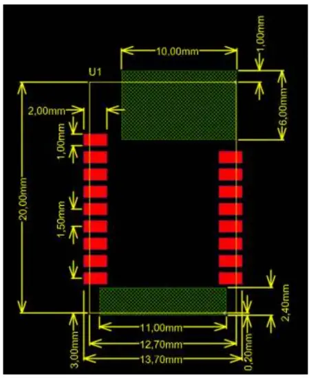
Vertical Mounting
The M7B-Q95-B module can be mounted in a vertical position by using the soldering pads on the short side of the module.
It can be soldered between pin rows of a 2-row 1.27mm pin header (2×8) or in slot on the base board with soldering pads at the edges of the slot.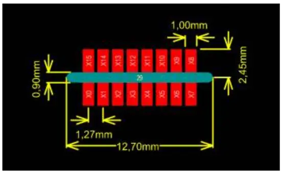
ELECTRICAL PARAMATERS
Absolut Maximum Ratings
| Absolut Maximum Ratings | Min | Max | Units |
| Supply voltage, VCC | -0.3 | 3.6 | V |
| I/O pin voltage | -0.3 | 3.6 | V |
| Input RF level, PMAX | +10 | dBm | |
| Storage temperature | °C | ||
| Operating temperature | -40 | +85 | °C |
| Soldering temperature | +260 | °C |
Recommended Operating Conditions
| Power Maximum Ratings | Min. | Typ. | Max. | Units |
| Supply voltage, VCC | 1.8 | 3.3 | 3.6 | V |
| Supply current, ICC | 12mA | V | ||
| Ambient Temperature, TA | -40 | 25 | 85 | °C |
General Purpose Input Output Specifications
Radio Characteristics
| Radio Characteristics | Min. | Typ. | Max. | Units |
| Operating frequency | 2405 | 2480 | MHz | |
| Maximum Output Power | 8 | dBm |
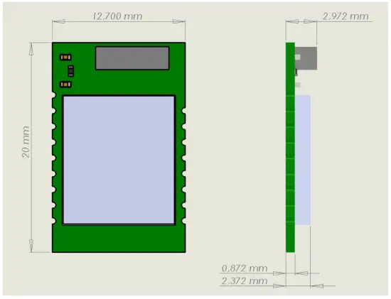
PHYSICAL DIMENSIONS
M7B-Q95-B
SOLDERING
Lead-free reflow soldering
Do not reflow solder with the module on the bottom side of the main PCB. The module might fall off the PCB during that process. Make sure that it is placed on the top side while reflow soldering.
Hand soldering
Hand soldering is possible. Follow IPC recommendations (reference document IPC-7711) when using a soldering iron.e
ORDERING INFORMATION
The following tables list the product variants available. Use the specified order code for your orders. Please contact ubisys support if you require any customization.
| Order Code | Part Name | Description |
| 1427 | M7B-Q95-B4 | ZigBee Light Application |
| x | ||
| x | ||
| x |
GENERAL TERMS & CONDITIONS OF BUSINESS
W hen placing your order you agree to be bound by our General Terms & Conditions of Business, http://www.ubisys.de/en/smarthome/terms.html
PRODUCT APPROVALS
Federal Communications Commission (FCC) Approvals
The ubisys M7B-Q95-B with integrated Antenna has been tested to comply with FCC CFR Part 15 (USA). This device complies with Part 15.247 of FCC Rules.
FCC statement:
This device complies with part 15 of the FC C Rules. Operation is subject to the following two conditions: (1) This device may not cause harmful interference, and
(2) this device must accept any interference received, including interference that may cause undesired operation.
FC C ID: 2AW GH-M7B-Q95-B
W hile the applicant for a device into which the M7B-Q95-B is installed is not required to obtain a new authorization for the module, this does not preclude the possibility that some other form of authorization or testing may be required for the end product.
The FCC requires the user to be notified that any changes or modifications made to this device that are not expressly approved by ubisys technologies GmbH may void the user’s authority to operate the equipment.
W hen using the M7B-Q95-B with approved antenna, it is required to prevent end-users from replacing them with non-approved ones.
Co-location of this module with other transmitter that operate simultaneously are required to be evaluated using the FCC multi-transmitter procedures.
If the host manufacturer uses the module in a Mobile configuration then the following text is placed in the host product, user guide:
- This device complies with FCC RF radiation exposure limits set forth for an uncontrolled environment, and must be installed with a separation distance of at least 20cm from all persons.
- If the RF exposure conditions are different after module integration into a host product (eg: Portable usage, or co-location with another transmitter/ antenna), the this text must be altered as appropriate
This modular transmitter is only FCC authorized for the specific rule parts (i.e., FCC transmitter rules) listed on the grant, and the host product manufacturer is responsible for compliance to any other FCC rules that apply to the host not covered by the modular transmitter grant of certification.
If the grantee markets their product as being Part 15 Subpart B compliant (when it also contains unintentional-radiator digital circuity), then the grantee shall provide a notice stating that the final host product still requires Part 15 Subpart B compliance testing with the modular transmitter installed
FCC Labelling Requirements
W hen integrating the M7B-Q95-B into a product it must be ensured that the FCC labelling requirements are met. This includes a clearly visible label on the outside of the finished product specifying the ubisys technologies GmbH FCC identifier (FCC ID: 2AW GH-M7B-Q95-B) as well as Transmitter Module FCC ID: 2AW GH-M7B-Q95-B 2AW GH-M7B-Q95-B although any similar wording that expresses the same meaning may be used.
Industry Canada (IC) Approvals
The ubisys technologies GmbH M7B-Q95-B with integrated antenna has been tested to comply with IC .
IC: 26146-M7BQ95B
PMN: BLEnd/Z M7B-Q95B
HVIN: B4
- Operation is subject to the following two conditions: (1) this device may not cause interference, and (2) this device must accept any interference, including interference that may cause undesired operation of the device.
- This module complies with FCC and Industry Canada RF radiation exposure limits set forth for general population. To maintain compliance, this module must not be co-located or operating in conjunction with any other antenna or transmitter.
The labelling requirements for Industry Canada are similar to those of the FCC. Again a clearly visibly
label must be placed on the outside of the finished product stating something like “Contains
Transmitter Module, IC: 26146-M7B095B”, although any similar wording that expresses the samemeaning may be used.
The integrator is responsible for the final product to comply to IC ICES-003 and FCC Part 15, Sub. B Unintentional Radiators
European Certification (ETSI)
The M7B-Q95-B has been certified to the following standards:
- Radio: EN 300 328 EMC:
- EN 301 489-1 & EN 301 489-17 Ver. 3.1.1
If the M7B-O95-B module is incorporated into an OEM product. the OEM product manufacturer must ensure compliance of the final product to the European Harmonised EMC, and low voltage/safety standards. A Declaration of Conformity must be issued for each of these standards and kept on file as described in Annex II of the R& TTE Directive. The final product must not exceed the specified power ratings, antenna specifications and installation requirements as specified in this user manual. If any of these specifications are exceeded in the final produc1 then a submission must be made to a notified body for compliance testing to all the required standards.
The ‘CE’ marking must be applied to a visible location on any OEM product. For more information
please refer to http://ec.europa.eu/enterprise/faq/ce-mark.htm. Customers assume full responsibility for learning and meeting the required guidelines for each country in their distribution market
DECLARATION OF CONFORMITY
Declarations of Conformity for the M7B-Q95-B module have been issued by ubisys technologies GmbH, which cover radio emissions, electromagnetic compatibility and immunity. These documents are available from our website or on request.
REVISION HISTORY
| Revision | Date | Remarks |
| 0.1 | 10/03/2020 | Initial Draft Version |
| 0.2 | 08/12/2020 | Physical dimensions added |
| 0.3 | 10/01/2020 | Product approvals defined more precisely |
CONTACT
UBISYS TECHNOLOGIES GMBH
NEUMANNSTRASSE 10
40235 DÜSSELDORF
GERMANY
T: + 49 (211) 54 21 55 – 00 F: + 49 (211) 54 21 55 – 99
www.ubisys.de | [email protected]


 Instruction Manual")


