UNIGRAF UCD-500 DisplayPort 2.0 Video Generator and Analyzer 
GENERAL
Reference Standards
- VESA DisplayPort v1.4a Link Layer Compliance Test Specification (Link CTS), Revision 1.0, June 12, 2019
- VESA® DisplayPort® DSC Link Layer Compliance Test Specification, Version 1.4a, Revision 1.1, Draft 6, Nov 18, 2019
- VESA® DisplayPort® DP 2.0 Link Layer Compliance Test Specification, Version 2.0, Revision 1.0, Phase 1, Draft 5, Aug 2, 2021
- High-bandwidth Digital Content Protection, Revision 2.3 on DisplayPort, Compliance Test Specification, Revision 1.1, 4 March 2019
Released Versions
This document explains features found in UCD Console version 2.3
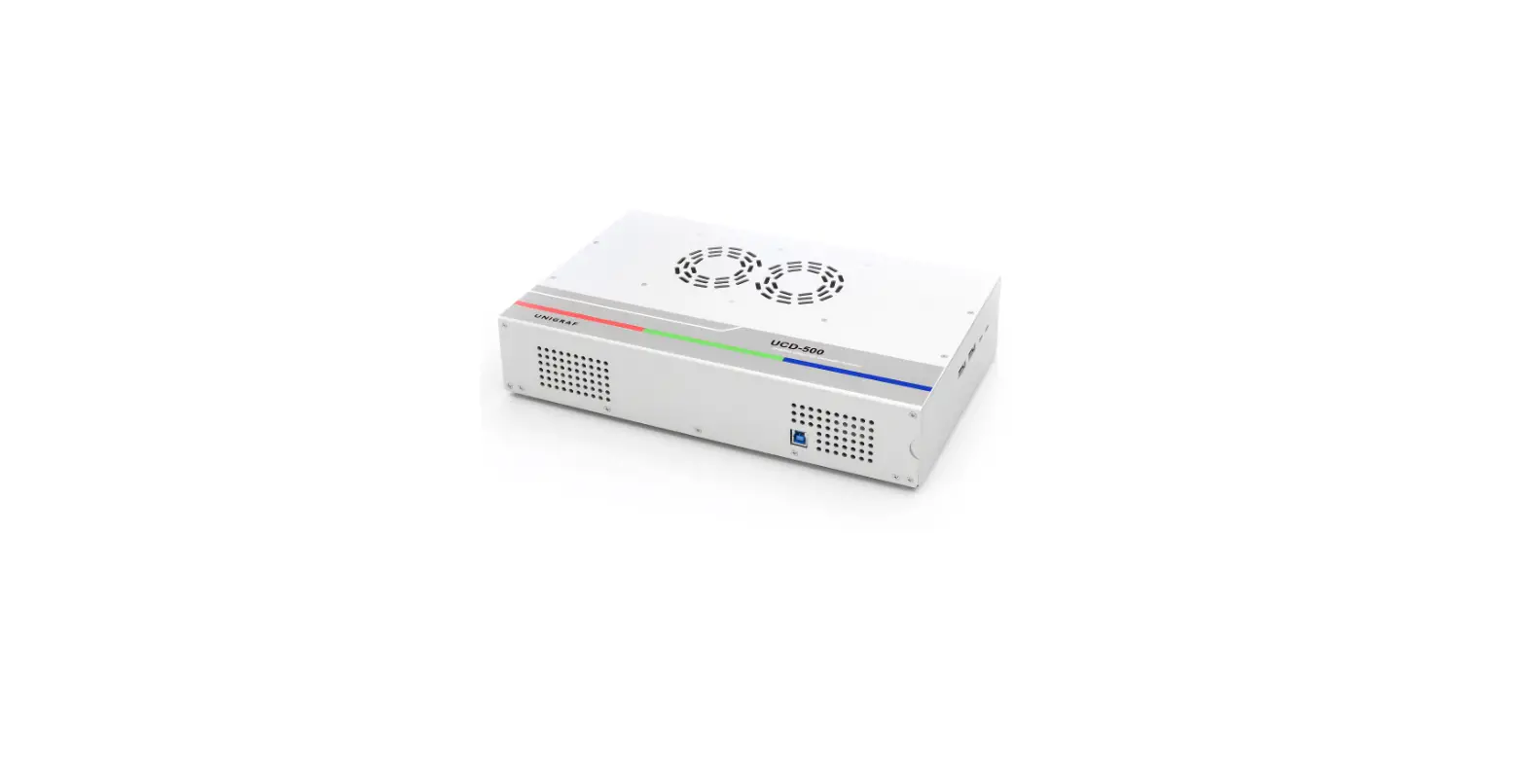
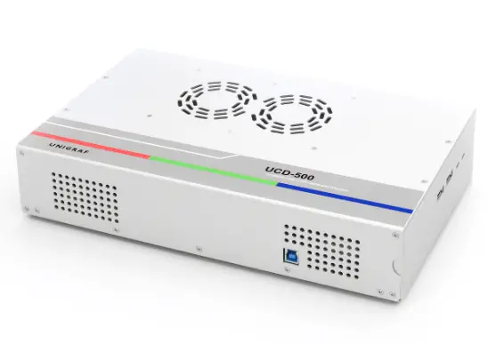
DP 2.0 Reference Hardware Products
| Product | P/N | Description |
| UCD-500 Tester | 066700 | DP 2.0 capable test unit for DisplayPort Sink and Source up to 10K@60Hz 24bpp. Support DP and USB-C connectors. USB 3.0 Interface to Host PC. |
DP Link CTS Test Software Product Options
| Product | P/N | Description |
| DP 1.4 LL CTS for testing Source DUT | MT6637 | DP 1.4 LL, FEC & Audio compliance tests for testing Source DUT. |
| DP 1.4 LL CTS for testing Sink DUT | MT6635 | DP 1.4 LL, FEC & Audio compliance tests for testing Sink DUT. |
| DP 2.0 LL CTS for testing Sink DUT | MT6660 | DP 2.0 LL compliance tests for testing Sink DUT. Audio, DSC and FEC CTS included. |
| DP 2.0 LL CTS for testing Source DUT | MT6662 | DP 2.0 LL compliance tests for testing Source DUT. Audio, DSC and FEC CTS included. |
| DP 1.4 DSC CTS for testing Source DUT | MT6642 | Display Stream Compression compliance tests for testing Source DUT. |
| DP 1.4 DSC CTS for testing Sink DUT | MT6643 | Display Stream Compression compliance tests for testing Sink DUT. |
| DP DisplayID & EDID CTS for testing Source DUT | MT6646 | DisplayID CTS for testing Source DUT. |
| DP DisplayID & EDID CTS for testing Sink DUT | MT6647 | DisplayID CTS for testing Sink DUT. |
| Adaptive-Sync CTS for testing Source DUT | MT6648 | Adaptive-Sync CTS for testing Source DUT. |
| Adaptive-Sync CTS for testing Sink DUT | MT6649 | Adaptive-Sync CTS for testing Sink DUT. |
Test Software Content 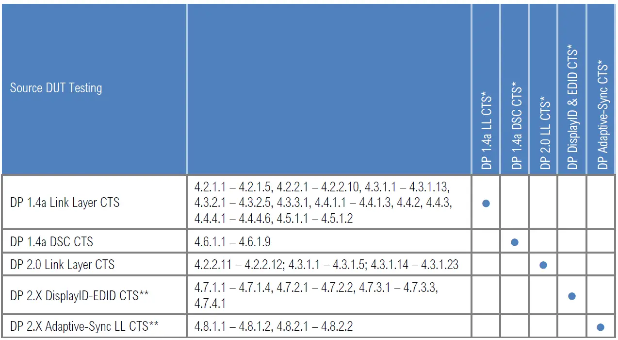
*) Separate licenses for testing Sink, Source, Branch (LL CTS, DSC, DisplayID) DUT
**) Unigraf UCD-400 was used by VESA for TE correlation of the tests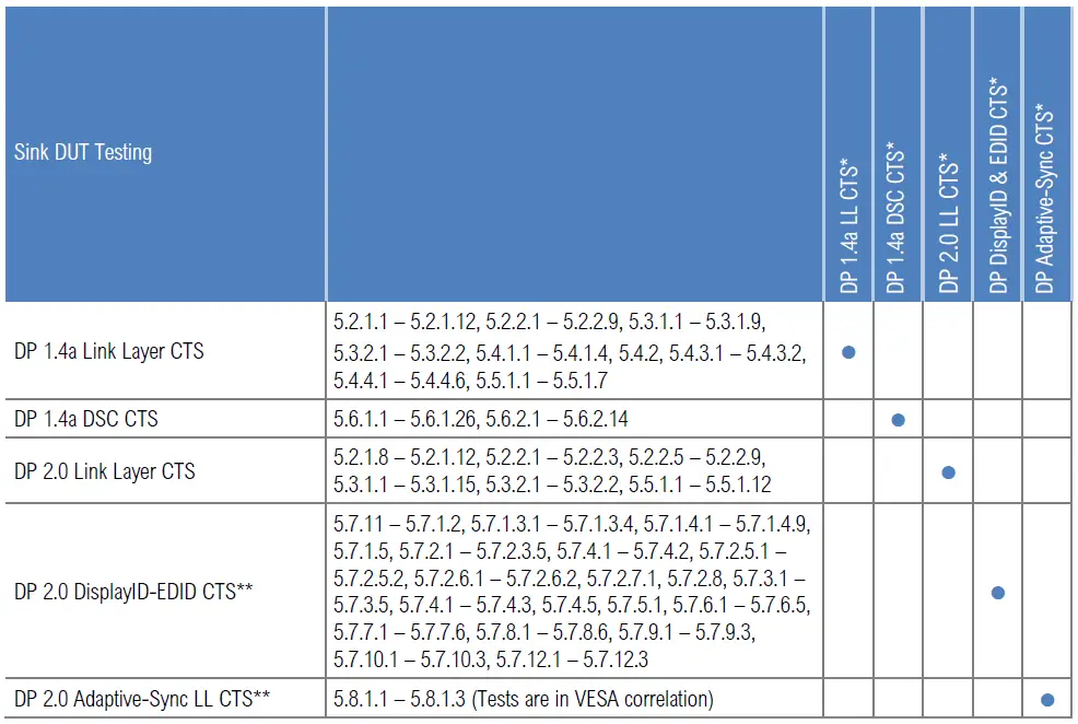 *) Separate licenses for testing Sink, Source, Branch (LL CTS, DSC, DisplayID) DUT
**) DP DisplayID / EDID CTS and Adaptive-Sync CTS will be supported in future versions of UCD-500
LINK CTS FOR TESTING SOURCE DUT
DP 1.4a LL CTS for testing Source DUT (P/N: MT6637)
AUX Reads after HPD Plug Event
| Test Reference | Test Name |
| 4.2.1.1 | Source DUT Retry on No-Reply During AUX Read after HPD Plug Event |
| 4.2.1.2 | Source Retry on Invalid Reply During AUX Read after HPD Plug Event |
| 4.2.1.3 | Source Device HPD Event Pulse Length Test |
| 4.2.1.4 | Source Device IRQ_HPD Pulse Length Test |
| 4.2.1.5 | Source Device Inactive HPD / Inactive AUX Test |
EDID and DPCD Reads
| 4.2.2.1 | DPCD Receiver Capability and EDID Read upon HPD Plug Event |
| 4.2.2.2 | DPCD Receiver Capability Read upon HPD Plug Event |
| 4.2.2.3 | EDID Read |
| 4.2.2.4 | EDID Read Failure #1: I2C-Over-AUX NACK |
| 4.2.2.5 | EDID Read Failure #2: I2C-Over-AUX DEFER |
| 4.2.2.6 | Source Device Inactive HPD / Inactive AUX test |
| 4.2.2.7 | Branch Device Detection upon HPD Plug Event |
| 4.2.2.8 | EDID Read on IRQ HPD Event after Branch Device Detection |
| 4.2.2.9 | E-DDC Four Block EDID Read |
| 4.2.2.10 | Link Status-Adjust Request AUX read interval during Link Training |
Link Training
| 4.3.1.1 | Successful Link Training at All Supported Lane Counts and Link Speeds |
| 4.3.1.2 | Successful Link Training Upon HPD Plug Event |
| 4.3.1.3 | Successful Link Training with Request of Higher Differential Voltage Swing During Clock Recovery Sequence |
| 4.3.1.4 | Successful Link Training to a Lower Link Rate #1: Iterate at Maximum Voltage Swing |
| 4.3.1.5 | Successful Link Training to a Lower Link Rate #2: Iterate at Minimum Voltage Swing |
| 4.3.1.6 | Successful Link Training with Request of a Higher Pre-emphasis Setting During Channel Equalization Sequence |
| 4.3.1.7 | Successful Link Training at Lower Link Rate Due to Loss of Symbol Lock During Channel Equalization Sequence |
| 4.3.1.8 | Unsuccessful Link Training at Lower Link Rate #1: Iterate at Maximum Voltage Swing |
| 4.3.1.9 | Unsuccessful Link Training at Lower Link Rate #2: Iterate at Minimum Voltage Swing |
| 4.3.1.10 | Unsuccessful Link Training due to Failure in Channel Equalization Sequence (loop count > 5) |
| 4.3.1.11 | Successful LT with Simultaneous Request for Differential Voltage Swing and Pre-emphasis during Clock Recovery Sequence |
| 4.3.1.12 | Source Device Link Training CR Fallback Test |
| 4.3.1.13 | Source Device Link Training EQ Fallback Test |
Link Maintenance
| Test Reference | Test Name |
| 4.3.2.1 | Successful Link Re-training After IRQ HPD Pulse Due to Loss of Symbol Lock |
| 4.3.2.2 | Successful Link Re-training After IRQ HPD Pulse Due to Loss of Clock Recovery Lock |
| 4.3.2.3 | Successful Link Re-training After IRQ HPD Pulse Due to Loss of Inter-lane Alignment Lock |
| 4.3.2.4 | Handling of IRQ HPD Pulse with No Error Status Bits Set |
| 4.3.2.5 | Lane Count Reduction |
Video Time Stamp Generation
| 4.3.3.1 | Video Time Stamp Generation |
Main Stream Data Mapping
| 4.4.1.1 | Pixel Data Packing and Steering |
| 4.4.1.2 | Main Stream Data Packing and Stuffing – Least Packed TU |
| 4.4.1.3 | Main Stream Data Packing and Stuffing – Most Packed TU |
| 4.4.2 | Main Video Stream Format Change Handling |
| 4.4.3 | Power Management |
Audio Stream Transmission over Secondary Packets
| 4.4.4.1 | Configuring Video and Audio Parameters |
| 4.4.4.2 | Audio Stream Header Synchronization |
| 4.4.4.3 | Audio Time Stamp Generation |
| 4.4.4.4 | Audio InfoFrame Packet |
| 4.4.4.6 | Audio Start Sequence |
Source FEC Protocol
| 4.5.1.1 | FEC enable verification for all supported Lane count and Link Speed |
| 4.5.1.2 | FEC ready verification for non FEC capable sink |
DP DSC 1.4 CTS for testing Sink DUT (P/N MT6642)
Source Device DSC Test Procedures
| Test Reference | Test Name |
| 4.6.1.1 | DSC enable sequence verification |
| 4.6.1.2 | DSC PPS block prediction flag verification |
| 4.6.1.3 | DSC PPS convert RGB flag verification |
| 4.6.1.4 | DSC PPS YCbCr 4:4:4 convert RGB = 0) flag verification |
| 4.6.1.5 | DSC PPS Simple 4:2:2 flag verification |
| 4.6.1.6 | DSC PPS Native 4:2:2 flag verification |
| 4.6.1.7 | DSC PPS Native 4:2:0 flag verification |
| 4.6.1.8 | DSC PPS convert RGB flag verification for DSC Algorithm Revision 1.1 |
| 4.6.1.9 | DSC PPS (YCbCr 4:4:4 convert RGB = 0) flag verification for DSC Algorithm Revision 1.1 |
DP 2.0 LL CTS for testing Source DUT (P/N: MT6637)
AUX Reads after HPD Plug Event
| Test Reference | Test Name |
| 4.2.2.11 | Various UHBR AUX read interval verification in first EQ loop |
| 4.2.2.12 | UHBR Link Status/Adjust different FFE Request, different AUX read interval for 10 EQ loop |
Link Training
| (4.3.1.1)* | Successful Link Training at All Supported Lane Counts and Link Speeds |
| (4.3.1.2)* | Successful Link Training Upon HPD Plug Event |
| (4.3.1.3)* | Successful Link Training with Request of Higher Differential Voltage Swing During Clock Recovery Sequence |
| (4.3.1.4)* | Successful Link Training to a Lower Link Rate #1: Iterate at Maximum Voltage Swing |
| (4.3.1.5)* | Successful Link Training to a Lower Link Rate #2: Iterate at Minimum Voltage Swing |
*) Test available. VESA Status: TE Correlation process not started
| 4.3.1.14 | Successful Link Training at All Supported Lane Counts and UHBR Link Speeds |
| 4.3.1.15 | Successful Link Training Upon HPD Plug Event for UHBR speed. |
| 4.3.1.16 | Successful Link Training when EQ done at 20th loop during channel EQ phase |
| 4.3.1.17 | Successful Link Training to a Lower Bandwidth, when CHANNEL_EQ_DONE bits not set in 20 loops during channel EQ phase |
| 4.3.1.18 | Successful Link Training to a Lower Bandwidth. When LT Failed received in middle of 20 loop (random value 1 to 19)* during channel EQ Done |
| 4.3.1.19 | Successful Link Training to a Lower Bandwidth. When LT Failed received at 20th loop during channel EQ Done |
| 4.3.1.20 | Successful Link Training to a Lower Bandwidth. When LT Failed received at after EQ done |
| 4.3.1.21 | Successful Link Training to a Lower Bandwidth. When EQ_INTERLANE_ALIGN_DONE bit not set during EQ phase |
| 4.3.1.22 | Successful Link Training to a Lower Bandwidth. When Symbols not locked during CDS phase. |
| 4.3.1.23 | Successful Link Training to a Lower Bandwidth. When CDS_INTERLANE_ALIGN_DONE bit not set during CDS phase. |
DisplayID – EDID CTS for testing Source DUT (P/N: MT6646)
Note: Unigraf UCD-400 was used by VESA for TE correlation of the tests
Video Tests
| Test Reference | Test Name |
| 4.7.1.1 | Basic Supported Formats |
| 4.7.1.2 | Preferred Timing |
| 4.7.1.3 | Out-of-Range Request |
| 4.7.1.4 | Invalid EDID |
Audio Tests
| 4.7.2.1 | Basic Supported Formats |
| 4.7.2.2 | Out-of-Range Request |
Source Device Test Procedures (E-DDC Protocol)
| 4.7.3.1 | EDID Read with More than 256 Bytes of Data Including DisplayID Block |
| 4.7.3.2 | EDID Read with Greater than 8 Blocks of Data Including DisplayID Block |
| 4.7.3.3 | EDID Read with Unknown Extensions and Unknown Data Blocks, Including DisplayID Block |
Source Device Test Procedures (DisplayID)
| 4.7.4.1 | DisplayID Detailed Timing support |
Source Device Test Procedures (Adaptive-Sync)
| (4.7.5.1)* | DisplayID Adaptive-Sync CVT RB Timing v3 Support |
*) Test available. VESA Status: In TE Correlation process
Adaptive-Sync CTS for testing Source DUT (P/N: MT6648)
Note: Unigraf UCD-400 was used by VESA for TE correlation of the tests
Fixed-Average VTotal Mode Support Validation
| Test Reference | Test Name |
| (4.8.1.1)* | Fixed-Average VTotal Mode Support over the Declared Frame Rate Range |
| (4.8.1.2)* | Fixed-Average VTotal Mode Duration Increase and Decrease Constraint Value Support |
*) Test available. VESA Status: In TE Correlation process
Adaptive VTotal Mode Support Validation
| (4.8.2.1)* | Adaptive VTotal Mode Support with Duration Increase and Decrease Constraint Values |
| (4.8.2.2)* | Adaptive VTotal Mode Support with Unconstrained Duration Increase and Decrease |
*) Test available. VESA Status: In TE Correlation process
LINK CTS FOR TESTING SINK DUT
DP 1.4a LL CTS for testing Sink DUT (P/N MT6635)
AUX Channel Protocol
| Test Reference | Test Name |
| 5.2.1.1 | Read One Byte from Valid DPCD Address |
| 5.2.1.2 | DPCD Receiver Capability Read (Read 12 Bytes from Valid DPCD Address) |
| 5.2.1.3 | Write One Byte to Valid DPCD Address |
| 5.2.1.4 | Write Nine Bytes to Valid DPCD Addresses |
| 5.2.1.5 | Write EDID Offset (One Byte I2C-Over-AUX Write) |
| 5.2.1.6 | Read One EDID Byte (One Byte I2C-Over-AUX Read) |
| 5.2.1.7 | EDID Read (1 Byte I2C -Over-AUX Segment Write, 1 Byte I2C-Over-AUX Offset Write, 128 Byte I2C- Over-AUX Read) |
| 5.2.1.8 | Illegal AUX Request Syntax |
| 5.2.1.9 | Glitch Rejection |
| 5.2.1.10 | Interleaved EDID and DPCD Receiver Capability Read |
| 5.2.1.11 | Downstream Stop on MOT Reset |
| 5.2.1.12 | Downstream Stop on Timeout |
Sink Device DPCD Field Implementation Addendum
| 5.2.2.1 | Sink Organizationally Unique Identifier (OUI) |
| 5.2.2.2 | Sink Count |
| 5.2.2.3 | Sink Status |
| 5.2.2.4 | Sink Error Count |
| 5.2.2.5 | DPCD Address Range |
| 5.2.2.6 | Number of Receiver Ports |
| 5.2.2.7 | Main Link Channel Coding |
| 5.2.2.8 | ESI Field Mapping |
| 5.2.2.9 | Sink Device Symbol Error Count |
Link Training
| Test Reference | Test Name |
| 5.3.1.1 | Successful Link Training at All Supported Lane Counts and Link Speeds |
| 5.3.1.2 | Successful Link Training with Request of Higher Differential Voltage Swing During Clock Recovery Sequence |
| 5.3.1.3 | Successful Link Training to a Lower Link Rate Due to Clock Recovery Lock Failure During Clock Recovery Sequence |
| 5.3.1.4 | Successful Link Training with Request of a Change to Pre-Emphasis and/or Voltage Swing Setting During Channel Equalization Sequence |
| 5.3.1.5 | Successful Link Training at Lower Link Rate Due to Loss of Symbol Lock During Channel Equalization Sequence |
| 5.3.1.6 | Lane Count Reduction |
| 5.3.1.7 | Lane Count Increase |
| 5.3.1.8 | 2-Lane Link Training CR/EQ Fallback Test |
| 5.3.1.9 | 1-Lane Link Training CR/EQ Fallback Test |
Link Maintenance
| 5.3.2.1 | IRQ HPD Pulse Due to Loss of Symbol Lock and Clock Recovery Lock |
| 5.3.2.2 | IRQ HPD Pulse Due to Loss of Inter-lane Alignment Lock |
Main Video Stream Reconstruction
| 5.4.1.1 | Pixel Data Reconstruction |
| 5.4.1.2 | Main Stream Data Unpacking and Unstuffing – Least Packed TU |
| 5.4.1.3 | Main Stream Data Unpacking and Unstuffing – Most Packed TU |
| 5.4.1.4 | Pixel ClockRecovery |
| 5.4.2 | Main Video Stream Format Change Handling |
| 5.4.3.1 | Entering and Exiting Power Save Mode |
| 5.4.3.2 | Resumption of Main Link Activity After Extended Idle |
Main Audio Stream Reconstruction
| 5.4.4.1 | Audio Test Patterns |
| 5.4.4.2 | Audio Startup and Format Change |
| 5.4.4.3 | RS Error Correction |
| 5.4.4.4 | Audio InfoFrame Packet |
| 5.4.4.5 | Audio Clock Recovery |
| 5.4.4.6 | Audio Stream Reception |
Sink FEC Protocol
| 5.5.1.1 | Sink Device FEC capability verification |
| 5.5.1.2 | Successful Link Training at All Supported Lane Counts and Link Rates with FEC Enable |
| 5.5.1.3 | Uncorrectable Block error count |
| 5.5.1.4 | Correctable Block error count |
| 5.5.1.5 | Correctable Bit error count |
| 5.5.1.6 | Correctable Parity Block error count |
| 5.5.1.7 | Correctable Parity Bit error count |
DP 1.4a DSC CTS For testing Sink DUT (P/N MT6643)
Sink Device DSC Test Procedures
| Test Reference | Test Name |
| 5.6.1.1 | DSC capability verification |
| 5.6.1.2 | DSC RGB Color Depth Test |
| 5.6.1.3 | DSC RGB Block Prediction Test |
| 5.6.1.4 | DSC RGB bits-per-pixel test |
| 5.6.1.5 | DSC RGB slice test |
| 5.6.1.6 | DSC RGB lane test |
| 5.6.1.7 | DSC YcbCr 4:4:4 Color Depth Test |
| 5.6.1.8 | DSC YcbCr 4:4:4 Block Prediction Test |
| 5.6.1.9 | DSC YcbCr 4:4:4 bits-per-pixel test |
| 5.6.1.10 | DSC YcbCr 4:4:4 slice test |
| 5.6.1.11 | DSC YcbCr 4:4:4 lane test |
| 5.6.1.12 | DSC Simple 4:2:2 Color Depth Test |
| 5.6.1.13 | DSC Simple 4:2:2 Block Prediction Test |
| 5.6.1.14 | DSC Simple 4:2:2 bits-per-pixel test |
| 5.6.1.15 | DSC Simple 4:2:2 slice test |
| 5.6.1.16 | DSC Simple 4:2:2 lane test |
| 5.6.1.17 | DSC Native 4:2:2 Color Depth Test |
| 5.6.1.18 | DSC Native 4:2:2 Block Prediction Test |
| 5.6.1.19 | DSC Native 4:2:2 bits-per-pixel test |
| 5.6.1.20 | DSC Native 4:2:2 slice test |
| 5.6.1.21 | DSC Native 4:2:2 lane test |
| 5.6.1.22 | DSC Native 4:2:0 Color Depth Test |
| 5.6.1.23 | DSC Native 4:2:0 Block Prediction Test |
| 5.6.1.24 | DSC Native 4:2:0 bits-per-pixel test |
| 5.6.1.25 | DSC Native 4:2:0 slice test |
| 5.6.1.26 | DSC Native 4:2:0 lane test |
Sink DSC Protocol Extension
| Test Reference | Test Name |
| 5.6.2.1 | DSC Height test |
| 5.6.2.2 | DSC Padding test |
| 5.6.2.3 | DSC RGB min and max bits-per-pixel test |
| 5.6.2.4 | DSC YcbCr 4:4:4 min and max bits-per-pixel test |
| 5.6.2.5 | DSC Simple 4:2:2 min and max bits-per-pixel test |
| 5.6.2.6 | DSC Native 4:2:2 min and max bits-per-pixel test |
| 5.6.2.7 | DSC Native 4:2:0 min and max bits-per-pixel test |
| 5.6.2.8 | DSC RGB most pack test |
| 5.6.2.9 | DSC Native 4:2:2 most pack test |
| 5.6.2.10 | DSC Native 4:2:0 most pack test |
| 5.6.2.11 | DSC one corrupt slice test |
| 5.6.2.12 | DSC interrupt test for Chunk Length error |
| 5.6.2.13 | DSC interrupt test for RC buffer under-run error |
| 5.6.2.14 | DSC interrupt test for RC buffer overflow error |
DP 2.0 LL CTS for testing Sink DUT (P/N MT6660)
AUX Channel Protocol
| Test Reference | Test Name |
| (5.2.1.8)* | Illegal AUX Request Syntax |
| (5.2.1.9)* | Glitch Rejection |
| (5.2.1.10)* | Interleaved EDID and DPCD Receiver Capability Read |
| (5.2.1.11)* | Downstream Stop on MOT Reset |
| (5.2.1.12)* | Downstream Stop on Timeout |
*) Test available. VESA Status: In TE Correlation process
Sink Device DPCD Field Implementation Addendum
| (5.2.2.1)* | Sink Organizationally Unique Identifier (OUI) |
| (5.2.2.2)* | Sink Count |
| (5.2.2.3)* | Sink Status |
| (5.2.2.5)* | DPCD Address Range |
| (5.2.2.6)* | Number of Receiver Ports |
| (5.2.2.7)* | Main Link Channel Coding |
| (5.2.2.8)* | ESI Field Mapping |
| (5.2.2.9)* | Sink Device Symbol Error Count |
*) Test available. VESA Status: In TE Correlation process
Link Training
| (5.3.1.1)* | Successful Link Training at All Supported Lane Counts and Link Speeds |
| (5.3.1.2)* | Successful Link Training with Request of Higher Differential Voltage Swing During Clock Recovery Sequence |
| (5.3.1.3)* | Successful Link Training to a Lower Link Rate Due to Clock Recovery Lock Failure During Clock Recovery Sequence |
| (5.3.1.4)* | Successful Link Training with Request of a Change to Pre-Emphasis and/or Voltage Swing Setting During Channel Equalization Sequence |
| (5.3.1.5)* | Successful Link Training at Lower Link Rate Due to Loss of Symbol Lock During Channel Equalization Sequence |
| (5.3.1.6)* | Lane Count Reduction |
| (5.3.1.7)* | Lane Count Increase |
| (5.3.1.8)* | 2-Lane Link Training CR/EQ Fallback Test |
| (5.3.1.9)* | 1-Lane Link Training CR/EQ Fallback Test |
| (5.3.1.10)* | Successful Link Training at All Supported Lane Counts and UHBR Link Speeds |
| (5.3.1.11)* | Successful Link Training to lower bandwidth, due to failure in EQ Phase of UHBR |
| (5.3.1.12)* | Successful Link Training to lower bandwidth, due to failure in CDS Phase of UHBR |
| (5.3.1.13)* | Successful Link Training to lower bandwidth, due to no start of CDS sequence Phase of UHBR Link Training |
| (5.3.1.14)* | 2-Lane UHBR Link Training EQ Fallback Test |
| (5.3.1.15)* | 1-Lane UHBR Link Training EQ Fallback Test |
*) Test available. VESA Status: In TE Correlation process
Link Maintenance
| Test Reference | Test Name |
| (5.3.2.1)* | IRQ HPD Pulse Due to Loss of Symbol Lock and Clock Recovery Lock |
| (5.3.2.2)* | IRQ HPD Pulse Due to Loss of Inter-lane Alignment Lock |
*) Test available. VESA Status: In TE Correlation process
Sink FEC protocol
| (5.5.1.1)* | Sink Device FEC capability verification |
| (5.5.1.2)* | Successful Link Training at All Supported Lane Counts and 8b10b Link Rates with FEC Enable |
| (5.5.1.3)* | Uncorrectable Block error count |
| (5.5.1.4)* | Correctable Block error count |
| (5.5.1.5)* | Correctable Bit error count |
| (5.5.1.6)* | Correctable Parity Block error count |
| (5.5.1.7)* | Correctable Parity Bit error count |
*) Test available. VESA Status: In TE Correlation process
DisplayID / EDID CTS for testing Sink DUT (P/N MT6647)
Note: Unigraf UCD-400 was used by VESA for TE correlation of the tests
EDID Block 0
| Test Reference | Test Name | |
| 5.7.1.1 | VESA E-EDID Verification Guide (Syntax Verification Only) | |
| 5.7.1.2 | Physical Display Characteristics |
EDID Block 0 (Basic Display Parameters and Features)
| 5.7.1.3.1 | Test for a Valid Video Input Definition |
| 5.7.1.3.2 | Test for a Valid Feature Support Byte |
| 5.7.1.3.3 | Test For Valid Established Timings I & II |
| 5.7.1.3.4 | Test For Valid Standard Timings |
18-Byte Descriptor Test Cases
| 5.7.1.4.1 | Test for Detailed Timing Descriptors |
| 5.7.1.4.2 | Test for Valid Display Descriptor Structure |
| 5.7.1.4.3 | Test for Valid Display Range Limits (tag #FDh) |
| 5.7.1.4.4 | Test for Valid Standard Timing Identifier Descriptor (tag #FAh) |
| 5.7.1.4.5 | Test for Valid CVT 3 Byte Code Descriptor (tag #F8h) |
| 5.7.1.4.6 | Test for Valid Established Timings III Descriptor (tag #F7h) |
| 5.7.1.4.7 | Test for Valid String Descriptors (tags #FFh, #FEh, #FCh) |
| 5.7.1.4.8 | Unused – Reserved Data Tag Number (Tags #11h to #F6h) |
| 5.7.1.4.9 | Test for Valid Dummy Descriptors (tag #10h) |
| 5.7.1.5 | Test for Valid Extension Flag and Checksum |
CTA Block Validation (CTA Extension Format)
| 5.7.2.1 | CEA Extension Version Number |
| 5.7.2.2 | Byte #2 (18-byte Descriptor Offset ‘d’) |
| 5.7.2.3.1 | Byte #3 – Underscan support |
| 5.7.2.3.2 | Byte #3 – Basic audio support |
| 5.7.2.3.3 | Byte #3 – YCbCr Support |
| 5.7.2.3.4 | Byte #3 – Native DTD Count |
| 5.7.2.3.5 | Byte #3 – Byte 3 Consistency |
Data Block Collection (Type Validation)
| 5.7.2.4.1 | Duplicate Data Block Validation |
| 5.7.2.4.2 | Validity of Data Block Types |
Short Video Descriptors (SVDs)
| 5.7.2.5.1 | Validity of SVDs |
| 5.7.2.5.2 | SVD/DTD Ordering |
Audio Data Block
| Test Reference | Test Name |
| 5.7.2.6.1 | Duplicate Audio Format Codes |
| 5.7.2.6.2 | Audio Output Validation |
Speaker Allocation Data Block
| 5.7.2.7.1 | Verify Max Number of Channels |
| 5.7.2.8 | Test for Detailed Timing Descriptors |
DisplayID Extension Block Framework Validation
| 5.7.3.1 | DisplayID EDID Extension Block Tag (Byte#0) and extension version (Byte#1) |
| 5.7.3.2 | DisplayID Section Size, Byte#2 |
| 5.7.3.3 | DisplayID Product Identifier/ Primary Use Case, Byte#3 |
| 5.7.3.4 | DisplayID Extension Count, Byte#4 |
| 5.7.3.5 | DisplayID Section Checksums |
DisplayID Extension Block Tiled Display Topology Block
| 5.7.4.1 | Block Revision (Byte#1) |
| 5.7.4.2 | Number of Payload Bytes in Block (Byte#2) |
| 5.7.4.3 | Tiled Display Capabilities (Byte#3, bit 6 and bit 7) |
| 5.7.4.5 | Tile Size (Byte#7 to Byte#10) |
DisplayID Extension with Stereo Display Interface Data Blocks
| 5.7.5.1 | Block Revision and Other Data (Byte #1) |
| 5.7.5.2 | Number of Payload Bytes in Block (Byte#2) |
DisplayID Extension with Type VII Detailed Timing Block
| 5.7.6.1 | Block Revision (Byte#1) |
| 5.7.6.2 | Block Number of Payload Bytes in Block (Byte#2) |
| 5.7.6.3 | Pixel Clock (Bytes #0 through #2 of each Descriptor) |
| 5.7.6.4 | Descriptor Payload Verification (Bytes #3 through #19 of each Descriptor) |
| 5.7.6.5 | Timing Support Validation |
DisplayID Extension with Type VIII Detailed Timing Block
| 5.7.7.1 | Block Revision and Other Data (Byte#1) |
| 5.7.7.2 | Block Number of Payload Bytes in Block (Byte#2) |
| 5.7.7.3 | DMT Timing Codes |
| 5.7.7.4 | CTA Timing Codes |
| 5.7.7.5 | HDMI Timing Codes |
| 5.7.7.6 | Timing Support Validation |
DisplayID Extension with Type IX Detailed Timing Block
| Test Reference | Test Name |
| 5.7.8.1 | Block Revision and Other Data (Byte#1) |
| 5.7.8.2 | Block Number of Payload Bytes in Block (Byte#2) |
| 5.7.8.3 | Timing Options (Byte #0 of each Descriptor) |
| 5.7.8.4 | Horizontal Active Image Pixels and Vertical Active Image Lines (Bytes #1-4 of each Descriptor) |
| 5.7.8.5 | Refresh Rate and Pixel Clock (Byte #5 of each Descriptor) |
| 5.7.8.6 | Timing Support Validation |
CTA Data Blocks in a DisplayID Extension
| 5.7.9.1 | Block Revision (Byte#1) |
| 5.7.9.2 | Block Number of Payload Bytes in Block (Byte#2) |
| 5.7.9.3 | Validity of Data Block Types |
DisplayID Vendor-Specific Data Blocks
| 5.7.10.1 | Block Revision (Byte#1) |
| 5.7.10.2 | Block Number of Payload Bytes in Block (Byte#2) |
| 5.7.10.3 | Manufacturer/Vendor ID Field |
Dynamic Video Timing Range Limits Data Block
| 5.7.11.1 | Block Revision (Byte#1) |
| 5.7.11.2 | Block Number of Payload Bytes in Block (Byte#2) |
| 5.7.11.3 | Minimum and Maximum Pixel Clock (Bytes #3 through #8) |
| 5.7.11.4 | Minimum and Maximum Vertical Refresh Rate (Bytes #9 and #10) |
| 5.7.11.5 | Dynamic Video Timing Range Support Flags (Byte #11) |
DisplayID Data Block Version Validation
| 5.7.12.1 | DisplayID Version 1.x Blocks |
| 5.7.12.2 | DisplayID Version 2.x Blocks |
| 5.7.12.3 | DisplayID Version 2.x Multiple Instances of Data Blocks |
Adaptive-Sync CTS for testing Sink DUT (P/N MT6649)
Note: Unigraf UCD-400 was used by VESA for TE correlation of the tests
Adaptive-Sync Operation Validation
| Test Reference | Test Name |
| (5.8.1.1)* | Fixed-Average VTotal Mode Support over the Declared Frame Rate Range |
| (5.8.1.2)* | Duration Increase and Decrease Constraint Value Support in Adaptive VTotal Mode |
| (5.8.1.3)* | Adaptive VTotal Mode Support |
*) Test available. VESA Status: In TE Correlation process
HDCP CTS FOR DISPLAYPORT
Note: With SW version 2.3 HDCP is supported only when 8b/10b link coding is enabled
DP HDCP 2.3 CTS Capable Hardware Products
| Product | P/N | Description |
| UCD-500 DP 2.0 Test Device | 066700 | DisplayPort™ 2.0 Video Generator and Analyzer unit for testing DisplayPort Sinks and Sources up to 8K@60Hz and 16K@60 Hz (with DSC) video modes with UHBR 20 Max Bit Rate Capability. |
DP HDCP 2.3 CTS Test Software Product Options
| Product | P/N | Description |
| DP HDCP 2.3 CTS for testing Source DUT | MT6634 | HDCP 2.3 on DisplayPort compliance tests for testing Source DUT. (Sets 1A + 1B) |
| DP HDCP 2.3 CTS for testing Sink DUT | MT6636 | HDCP 2.3 on DisplayPort compliance tests for testing Sink DUT. (Set 2C) |
| DP HDCP 2.3 CTS for testing Sink, Source and Repeater DUT | MT6638 | HDCP 2.3 on DisplayPort CTS for testing Sink, Source and Repeater DUT. (Sets 1A + 1B + 2C + 3A + 3B + 3C) |
Description of HDCP 2.3 CTS Tests
Note: With SW version 2.3 HDCP is supported only when 8b/10b link coding is enabled
DP HDCP 2.3 CTS for testing Source DUT (P/N MT6634)
1A. Downstream procedure with Receiver
| Test Reference | Test Name |
| HDCP2.3 CTS 1A-01 | Regular Procedure – With previously connected Receiver (With stored km) |
| HDCP2.3 CTS 1A-02 | Regular Procedure – With newly connected Receiver (Without stored km) |
| HDCP2.3 CTS 1A-03 | Regular Procedure – Receiver disconnect after AKE_Init |
| HDCP2.3 CTS 1A-04 | Regular Procedure – Receiver disconnect after km |
| HDCP2.3 CTS 1A-05 | Regular Procedure – Receiver disconnect after locality check |
| HDCP2.3 CTS 1A-06 | Regular Procedure – Receiver disconnect after ks |
| HDCP2.3 CTS 1A-07 | Regular Procedure – Receiver sends REAUTH_REQ after ks |
| HDCP2.3 CTS 1A-08 | Irregular Procedure – Verify Receiver Certificate |
| HDCP2.3 CTS 1A-09 | Irregular Procedure – SRM |
| HDCP2.3 CTS 1A-10 | Irregular Procedure – Invalid H’ |
| HDCP2.3 CTS 1A-11 | Irregular Procedure – Pairing Failure |
| HDCP2.3 CTS 1A-12 | Irregular Procedure – Locality Failure |
1B. Downstream procedure with Repeater
| HDCP2.3 CTS 1B-01 | Regular Procedure – With Repeater |
| HDCP2.3 CTS 1B-02 | Irregular Procedure – Timeout of Receiver ID list |
| HDCP2.3 CTS 1B-03 | Irregular Procedure – Verify V’ |
| HDCP2.3 CTS 1B-04 | Irregular Procedure – MAX_DEVS_EXCEEDED |
| HDCP2.3 CTS 1B-05 | Irregular Procedure – MAX CASCADE_EXCEEDED |
| HDCP2.3 CTS 1B-06 | Irregular Procedure – Incorrect seq_num_V |
| HDCP2.3 CTS 1B-07 | Regular Procedure – Re-authentication on HPD |
| HDCP2.3 CTS 1B-08 | Regular Procedure – Re-authentication on REAUTH_REQ |
| HDCP2.3 CTS 1B-09 | Irregular Procedure – Rollover of seq_num_V |
| HDCP2.3 CTS 1B-10 | Irregular Procedure – Failure of Content Stream Management |
DP HDCP 2.3 CTS for testing Sink DUT (P/N MT6636)
Note: With SW version 2.3 HDCP is supported only when 8b/10b link coding is enabled
2C. Upstream procedure with Transmitter
| Test Reference | Test Name |
| HDCP2.3 CTS 2C-01 | Regular Procedure – With transmitter |
| HDCP2.3 CTS 2C-02 | Irregular Procedure – New Authentication after AKE_Init |
| HDCP2.3 CTS 2C-03 | Irregular Procedure – New Authentication during Locality Check |
| HDCP2.3 CTS 2C-04 | Irregular Procedure – New Authentication after SKE_Send_Eks |
| HDCP2.3 CTS 2C-05 | Irregular Procedure – New Authentication during Link Synchronization |
| HDCP2.3 CTS 2C-06 | Regular Procedure – Encryption Disable Bootstrapping |
DP HDCP 2.3 CTS for testing Sink, Source and Repeater DUT (P/N MT6638)
Note: With SW version 2.3 HDCP is supported only when 8b/10b link coding is enabled
1A. Downstream procedure with Receiver
Please see above
1B. Downstream procedure with Repeater
Please see above
2C. Upstream procedure with Transmitter
Please see above
3A. Downstream procedure with Receiver
| Test Reference | Test Name |
| HDCP2.3 CTS 3A-01 | Regular Procedure – With previously connected Receiver (With stored km) |
| HDCP2.3 CTS 3A -02 | Regular Procedure – With newly connected Receiver (Without stored km) |
| HDCP2.3 CTS 3A -03 | Irregular Procedure – Verify Receiver Certificate |
| HDCP2.3 CTS 3A -04 | Irregular Procedure – invalid H’ |
| HDCP2.3 CTS 3A -05 | Irregular Procedure – Pairing Failure |
| HDCP2.3 CTS 3A -06 | Irregular Procedure – Locality Failure |
3B. Downstream Procedure with Repeater
| HDCP2.3 CTS 3B-01 | Regular Procedure – With Repeater |
| HDCP2.3 CTS 3B -02 | Irregular Procedure – Timeout of Receiver ID Iist |
| HDCP2.3 CTS 3B -03 | Irregular Procedure – Verify V’ |
| HDCP2.3 CTS 3B -04 | Irregular Procedure – MAX_DEVS_EXCEEDED |
| HDCP2.3 CTS 3B -05 | Irregular Procedure – MAX_CASCADE_EXCEEDED |
| HDCP2.3 CTS 3B -06 | Irregular Procedure – Rollover of seq_num_V |
| HDCP2.3 CTS 3B -07 | Irregular Procedure – Failure of Content Stream Management |
3C. Downstream Procedure with Transmitter
| Test Reference | Test Name |
| HDCP2.3 CTS 3C-01 | Regular Procedure – Transmitter – DUT – Receiver |
| HDCP2.3 CTS 3C -02 | Regular Procedure – Receiver Disconnect Propagation when an Active Receiver is Disconnected Downstream |
| HDCP2.3 CTS 3C -03 | Regular Procedure – Receiver Connected when an Active Receiver is Connected Downstream |
| HDCP2.3 CTS 3C -04 | Irregular Procedure – New Authentication after AKE_init |
| HDCP2.3 CTS 3C -05 | Irregular Procedure – New Authentication during Locality Check |
| HDCP2.3 CTS 3C -06 | Irregular Procedure – New Authentication after SKE_Send_Eks |
| HDCP2.3 CTS 3C -07 | Irregular Procedure – New Authentication during Link Synchronization |
| HDCP2.3 CTS 3C -08 | Irregular Procedure – Rx Certificate invalid |
| HDCP2.3 CTS 3C -09 | Irregular Procedure – invalid H’ |
| HDCP2.3 CTS 3C -10 | Irregular Procedure – Locality Failure |
| HDCP2.3 CTS 3C-11 | Regular Procedure – Transmitter – DUT – Repeater (With stored km) |
| HDCP2.3 CTS 3C-12 | Regular Procedure – Receiver disconnect after AKE_Init |
| HDCP2.3 CTS 3C-13 | Regular Procedure – Receiver disconnect after km |
| HDCP2.3 CTS 3C-14 | Regular Procedure – Receiver disconnect after Iocality check |
| HDCP2.3 CTS 3C-15 | Regular Procedure – Receiver disconnect after Ks |
| HDCP2.3 CTS 3C-16 | Irregular Procedure – Timeout of Receiver ID Iist |
| HDCP2.3 CTS 3C-17 | Irregular Procedure – Verify V’ |
| HDCP2.3 CTS 3C-18 | Irregular Procedure – DEVICE_COUNT |
| HDCP2.3 CTS 3C-19 | Irregular Procedure – DEPTH |
| HDCP2.3 CTS 3C-20 | Irregular Procedure – MAX_DEVS_EXCEEDED |
| HDCP2.3 CTS 3C-21 | Irregular Procedure – MAX_CASCADE_EXCEEDED |
| HDCP2.3 CTS 3C-22 | Regular Procedure – Repeater with zero downstream device |
| HDCP2.3 CTS 3C-23 | Regular Procedure – Propagation of HDCP2_0_REPEATER_DOWNSTREAM flag |
| HDCP2.3 CTS 3C-24 | Regular Procedure – Propagation of HDCP1_DEVICE_DOWNSTREAM flag |
| HDCP2.3 CTS 3C-25 | Regular Procedure – Content Stream Management |


