GOWIN IPUG781-1.5.1E USB 2.0 SoftPHY IP

All other words and logos identified as trademarks or service marks are the property of their respective holders. No part of this document may be reproduced or transmitted in any form or by any denotes, electronic, mechanical, photocopying, recording or otherwise, without the prior written consent of GOWINSEMI.
Disclaimer
GOWINSEMI assumes no liability and provides no warranty (either expressed or implied) and is not responsible for any damage incurred to your hardware, software, data, or property resulting from usage of the materials or intellectual property except as outlined in the GOWINSEMI Terms and Conditions of Sale. GOWINSEMI may make changes to this document at any time without prior notice. Anyone relying on this documentation should contact GOWINSEMI for the current documentation and errata.
Revision History
| Date | Version | Description |
| 07/23/2021 | 1.0E | Initial version published. |
| 08/13/2021 | 1.1E | The property configuration of IO ports modified. |
| 10/12/2021 | 1.2E | Chapter 2.3 “Using 5V Host Supply to Power USB Device Solution” added. |
| 12/23/2021 | 1.3E | l The configuration method of peripheral circuit modified. l IO configuration constraints added. |
| 03/29/2022 | 1.4E | The description of resource utilization added. |
| 06/20/2022 | 1.5E | l The speed grade modified. l The description of pin constraints updated. |
| 07/20/2022 | 1.5.1E | A note added in Table 2-1. |
Purpose
The purpose of Gowin USB 2.0 SoftPHY IP User Guide is to help you learn the features and usage of this IP by providing descriptions of functions, signals, and interface configuration.
The latest user guides are available on the GOWINSEMI Website. You can find the related documents at: www.gowinsemi.com.
- DS100, GW1N series of FPGA Products Data Sheet
- DS117, GW1NR series of FPGA Products Data Sheet
- DS821, GW1NS series of FPGA Products Data Sheet
- DS871, GW1NSE series of FPGA Products Data Sheet
- DS861, GW1NSR series of FPGA Products Data Sheet
- DS891, GW1NRF series of FPGA Products Data Sheet
- DS881, GW1NSER series of Bluetooth FPGA Products Data Sheet
- DS102, GW2A series of FPGA Products Data Sheet
- DS226, GW2AR series of FPGA Products Data Sheet
- DS961, GW2ANR series of FPGA Products Data Sheet
- DS976, GW2AN-55 Data Sheet
- DS971, GW2AN-18X & 9X Data Sheet
- SUG100, Gowin Software User Guide
Terminology and Abbreviations
The terminology and abbreviations used in this manual are as shown in Table 1-1.
| Terminology and Abbreviations | Meaning |
| IP | Intellectual Property |
| USB | Universal Serial Bus |
| UTMI | USB 2.0 Transceiver Macrocell Interface |
| HS | High Speed |
| FS | Full Speed |
| LS | Low Speed |
| NRZI | Non Return Zero Inverted |
Support and Feedback
Gowin Semiconductor provides customers with comprehensive technical support. If you have any questions, comments, or suggestions, please feel free to contact us directly by the following ways.
- Website: www.gowinsemi.com E-mail: [email protected]
Introduction
Gowin USB 2.0 SoftPHY IP is a USB physical layer transceiver that can support data reception and transmission at high speed (480Mbps), full speed (12Mbps), and low speed (1.5Mbps). Table 2-1 Gowin USB 2.0 SoftPHY IP Overview
| Gowin USB 2.0 SoftPHY IP | |
| IP Core Application | |
|
Supported Devices[1] | l Arora family l LittleBee family, excluding GW1N-1/GW1N-1S/GW1NZ-1/GW1N-1P5 devices.. |
| Logic Resource | Please refer to Table 2-3 and Table 2-4. |
| Delivered Doc. | |
| Design Files | Verilog (encrypted) |
| Reference Design | Verilog |
| TestBench | Verilog |
| Test and Design Flow | |
| Synthesis Software | GowinSynthesis |
| Application Software | Gowin Software (V1.9.8.05 and above) |
Note!
[1] Only part number with speed grade C7 and above support USB 2.0 SoftPHY IP
Features
The features of GowinUSB 2.0 SoftPHY IP include:
- Supports HS (480 Mbps), FS (12 Mbps), and LS (1.5 Mbps).
- Supports data serial and parallel conversion.
- Supports bit stuffer and unstuffed.
- Supports NRZI encoder and decoder.
- Supports UTMI interface.
Using 5V Host Supply to Power USB Device Solution
Many solutions may to provide power to a USB device using the 5V provided over the cable from the Host without providing a separate power supply. To support cable powered USB device use cases, designers must be careful to ensure the total PCB BOM of the device does not exceed the current limitations of the USB Host as well as voltage drops over the cable.The USB v2.0 specification, sections 7.1.2 and 7.3.2 provides information on current and voltage drop requirements expected to be supplied by a USB Host. If the total PCB BOM cannot meet the current and minimum voltage requirements of the specified host, the board can be powered with a separate power supply. Table 2-2 DC Electrical Characteristics
| Parameter | Symbol | Condition | Min. | Max. | Unit |
| Supply voltage | |||||
| High-power Port | VBUS | Note 2, Section 7.2.1 | 4.75 | 5.25 | V |
| Low-power Port | VBUS | Note 2, Section 7.2.1 | 4.40 | 5.25 | V |
| Supply Current | |||||
| High-power Hub Port (out) | ICCPRT | Section 7.2.1 | 500 | mA | |
| Low-power Hub Port (out) | ICCUPT | Section 7.2.1 | 100 | mA | |
| High-Power Function (in) | ICCHPF | Section 7.2.1 | 500 | mA | |
| Low-power Function (in) | ICCLPF | Section 7.2.1 | 100 | mA | |
| Unconfigured Function/Hub (in) | ICCINIT | Section 7.2.1.4 | 100 | mA | |
| Suspended High-power | ICCSH | Note 15, Section | 2.5 | mA | |
| Device | 7.2.3 | ||||
| Suspended Low-power Device | ICCSL | Section 7.2.3 | 500 | µA |
Resource Utilization
Gowin USB 2.0 SoftPHY IP can be implemented by Verilog. Its resource utilization may vary when the design is employed in different devices, or at different densities, speeds, or grades. Taking Gowin GW1NSR-4 and GW2AR-18 series of FPGA products as an instance, the resource utilization is as shown in Table 2-3 and Table 2-4. Table 2-3 Resource Utilization (І)
| Device | Speed Grade | Resource | Utilization | Notes |
|
GW1NSR-4 |
C7/I6 | LUT | 384 |
– |
| REG | 1109 | |||
| ALU | 13 | |||
| BSRAM | 1 | |||
| SSRAM | 0 | |||
| IO | 7 |
| Device | Speed Grade | Resource | Utilization | Notes |
|
GW2AR-18 |
C7/I6 | LUT | 384 |
– |
| REG | 1109 | |||
| ALU | 13 | |||
| BSRAM | 1 | |||
| SSRAM | 4 | |||
| IO | 7 |
Note!
GW2A series and GW1NSR-4 can choose the chip with speed grade C6/I5; for other part numbers, please choose the chip with speed grade C7/I6.
Functional Description
In the RX, after USB serial data goes through IDES8, NRZI decoder, bit unstuffer, shift Reg modules in turn, USB RX data is received, and then the data transmits to the upper module through UTMI interface. In the TX, after receiving the data transmitted by UTMI and then going through shift Reg, bit stuffer, NRZI encoder to generate the serial TX data stream, which then is sent to the USB interface via OSER8.Figure 3-1 USB 2.0 SoftPHY Block Diagram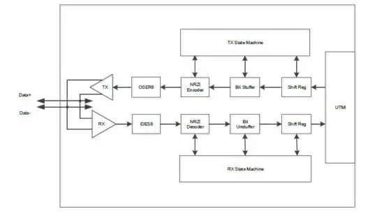
USB 2.0 SoftPHY External Circuit Connection
USB 2.0 SoftPHY supports high speed mode (480Mbps) . When the USB 2.0 SoftPHY is used as a USB slave device, the external circuit connection is as follows. Figure 3-2 USB Slave Device Interface Implementation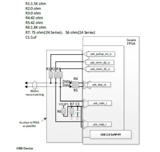
- You can see the followings for the IO port attribute constraints of GW2A series of FPGA.
- usb_dxp_io: IO_TYPE= LVCMOS33D PULL_MODE= NONE DRIVE=4;
- usb_term_dn_o: IO_TYPE=LVCMOS33 PULL_MODE= NONE DRIVE=8;
- usb_term_dp_o: IO_TYPE=LVCMOS33 PULL_MODE=NONE DRIVE=8;
- usb_pullup_en_o: IO_TYPE=LVCMOS33 PULL_MODE=NONE DRIVE=8;
- usb_rxdn_i: IO_TYPE=LVDS25 PULL_MODE=NONE;
- usb_rxdp_i: IO_TYPE=LVDS25 PULL_MODE=NONE.
- You can see the followings for the IO port attribute constraints of GW1N series of FPGA.
- usb_dxp_io: IO_TYPE= LVCMOS33D PULL_MODE= NONE DRIVE=8;
- usb_term_dn_o: IO_TYPE=LVCMOS33 PULL_MODE= NONE DRIVE=16;
- usb_term_dp_o: IO_TYPE=LVCMOS33 PULL_MODE= NONE DRIVE=16;
- usb_pullup_en_o: IO_TYPE=LVCMOS33 PULL_MODE= NONE DRIVE=8;
- usb_rxdn_i: IO_TYPE=LVDS25 PULL_MODE=NONE;
- usb_rxdp_i: IO_TYPE=LVDS25 PULL_MODE=NONE.
- All signals related to the USB interface on the FPGA are recommended to be placed in one Bank, using adjacent assignment, and powering the I/O Bank at 3.3V
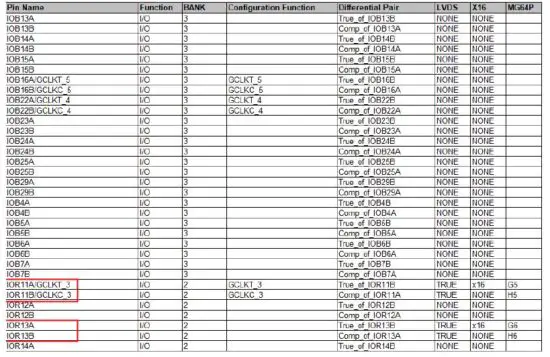
- It is required that the adjacent differential pair pins in the same Bank where the usb_dxp_io differential pair is located exist and are not used. Taking GW1NSR-4 as an example, Figure 3-3 shows the GW1NSR-4 Pinout. If the usb_dxp_io differential pair is located at G5, H5 (i.e. IOR11A/IOR11B) in the diagram, it will cause the project to report an error when implementing synthesis and placement with Gowin Software, as the adjacent differential pair pins IOR10A/IOR10B do not exist. If usb_dxp_io differential pair is located at G6/H6 (i.e. IOR13A/IOR13B), the project will synthesize and place successfully with Gowin Software, as the adjacent differential pair pins IOR12A/IOR12B exists.

Signal Description
A description of Gowin USB 2.0 SoftPHY IP signals is as shown in Table 4-1.
| No. | Signal Name | I/O | Data Width | Description |
| 1 | clk_i | I | 1 | Input clock signal (60MHz) |
| 2 | fclk_i | I | 1 | Input clock signal (480MHz) |
| 3 | rst_i | I | 1 | Asynchronous reset signal resets the state machine inside of PHY. |
| 4 | pll_locked_i | I | 1 | pll lock signal generating fclk_i |
| 5 | utmi_data_out_i | I | 8 | Data input, 8-bit parallel data transmit bus. |
| 6 | utmi_txvalid_i | I | 1 | Transmit data valid indicator, active-high. |
|
7 |
utmi_txready_o |
O |
1 | Transmit data ready signal, indicating that PHY can receive the data to be transmitted from the controller end. |
| 8 | utmi_data_in_o | O | 8 | Data output, 8-bit parallel data receive bus. |
| 9 | utmi_rxactive_o | O | 1 | Rx data active, indicating that PHY detects the SYNC signal and then starts receiving data. |
| 10 | utmi_rxvalid_o | O | 1 | Rx data valid, active-high. |
| 11 | utmi_rxerror_o | O | 1 | Receive data error, active high indicates receive error. |
| No. | Signal Name | I/O | Data Width | Description |
|
12 |
utmi_linestate_o |
O |
2 | Line status of receive end: DM DP 2’b00:SE0 2’b01:”J” 2’b10:”K” 2’b11:SE1 |
|
13 |
utmi_opmode_i |
I |
2 | Operation mode selection signal: 2’b00: Normal 2’b01: No driver 2’b10: Disable bit stuffing and NRZI encoding 2’B11: Reserved |
|
14 |
utmi_xcvrselect_i |
I |
2 | Transfer mode selection signal: 2’b00: HS Transfer 2’b01: FS Transfer 2’b10: LS Transfer 2’B11: Reserved |
| 15 | utmi_termselect_i | I | 1 | Termination Selection: 1’ b0: HS termination enable 1’ b1: FS / LS termination enable |
| 16 | usb_dxp_io | I/O | 1 | USB data signal Data+ |
| 17 | usb_dxn_io | I/O | 1 | USB data signal Data- |
| 18 | usb_rxdp_i | I | 1 | USB data signal Data+ input |
| 19 | usb_rxdn_i | I | 1 | USB data signal Data- input |
| 20 | usb_pullup_en_o | O | 1 | 1.5K resistor pull-up control on USB data signal Data+ |
| 21 | usb_term_dp_o | I/O | 1 | Termination resistor control of USB data signal Data+ |
| 22 | usb_term_dn_o | I/O | 1 | Termination resistor control of USB data signal Data- |
Interface Configuration
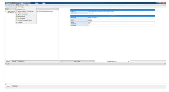
Selecting “Tools > IP Core Generator” in Gowin Software, you call and configure USB 2.0 SoftPHY.
- Open IP Core Generator After creating the project, you can click the “Tools” tab in the upper left, select and open the IP Core Generator via the drop-down list, as shown in Figure 5-1. Figure 5-1 IP Core Generator

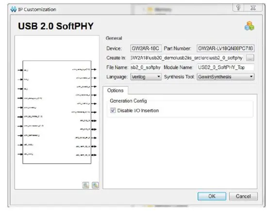
- Open USB 2.0 SoftPHY IP Core Select “Soft IP Core > Interface and Interconnect > USB 2.0 IP”, as shown in Figure 5-2. Double-click to open the configuration interface.

- USB 2.0 SoftPHY IP Core Configuration Interface Figure 5-3 shows the USB 2.0 SoftPHY IP core configuration interface. The ports diagram is on the left of the configuration interface. Options are on the right.