SRF NRM7292D Ultra Low Power and Long Range WiFi Module
Overview
IEEE 802.11ah is a new Wi-Fi standard operating in the Sub 1GHz license-exempt band, offering longer range and lower power connectivity necessary for internet of things (IoT) applications. NRM7292D contains external RF front end module (FEM) which can increase transmission power up to 23 dBm. Onboard serial flash can be used for OTA software development and with internal 32KB cache memory, it can support execution in place (XIP) feature.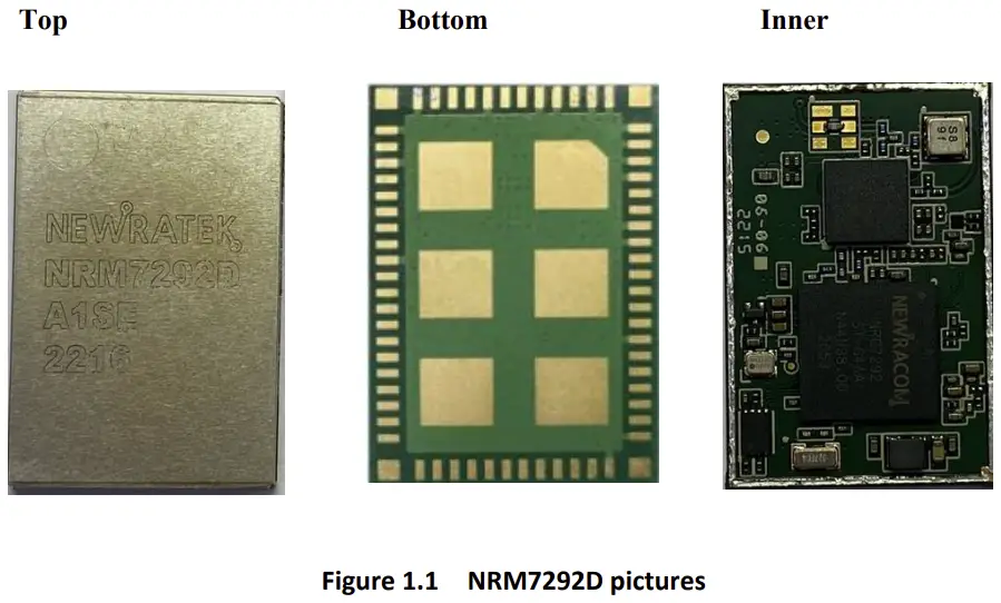
Applications
Low to high data rate of NRM7292D can be applied in various IoT applications like:
- Wearable
- Home automation
- Healthcare
- Industrial automation
- Safety and security
- Smart grid
- Multimedia streaming
NRM7292D module features
The main features of NRM7292D are represented as follows:
- Standard
- IEEE Std 802.11ahTM-2016 compliant
- 1/2/4 MHz channel bandwidth support
- WPA2 PSK support
- 150 Kbps ~ 15 Mbps data rate
- AP and STA role support
- Radio frequency
- 109 dBm minimum receive sensitivity
- +23 dBm transmit power
- 902~928 MHz frequency band (By replacing RF SAW filter, other frequency band can be supported within 750~950 MHz)
- CPU
- ARM Cortex-M3 for application
- ARM Cortex-M0 for IEEE 802.11ah WLAN
- Clock frequencies for both processor (32/48 MHz)
- Host interface
- UART and SPI support for host interface
- Peripherals
- GPIO, ADC, PWM and timers
- I2C, SPI and UART
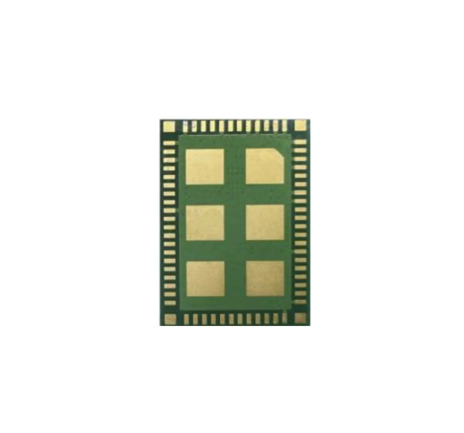
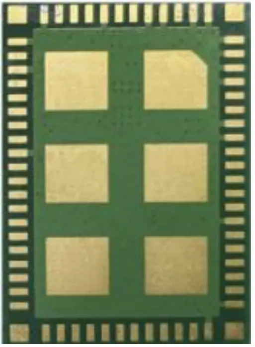
Pin Description
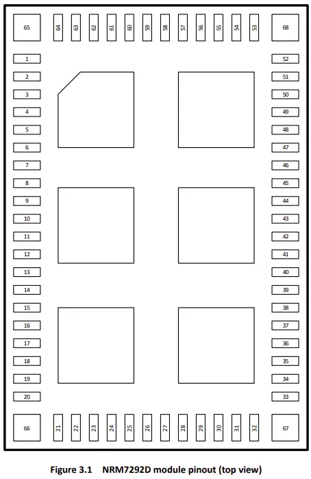
Table 3.1 NRM7292D signal description
Pad No | Name | Direction | Volt | Description |
| 1 | GROUND | GND | ||
2 | GROUND | GND | ||
| 3 | GROUND | GND | ||
4 | GROUND | GND | ||
| 5 | VDD_FEM | P | Front End Module power input | |
6 | VBAT | P | NRC7292 power input | |
| 7 | GROUND | GND | ||
8 | GROUND | GND | ||
| 9 | MODE_00 | I | SW Define (When ROM BOOT) 11: Internal SRAM BOOT | |
10 | MODE_01 | I | ||
11 | MODE_02 | I | 0: ROM BOOT | |
12 | MODE_03 | I | 0: Cortex-M0 Master | |
13 | MODE_04 | I | 0: Two CPU | |
14 | GROUND | GND | ||
15 | HSPI_nCS | I | Host SPI – Chip Select (active low) | |
| 16 | HSPI_CLK | I | Host SPI – Clock | |
17 | HSPI_MISO | O | Host SPI – Master in Slave out | |
| 18 | HSPI_MOSI | I | Host SPI – Master out Slave in | |
19 | HSPI_EIRQ | O | Host SPI – Interrupt | |
| 20 | GROUND | GND | ||
21 | GROUND | GND | ||
| 22 | NC | – | ||
23 | NC | – | ||
| 24 | NC | – | ||
25 | GP_00_UART2_TX | I/O | UART Channel2 Tx | |
| 26 | GP_01_UART2_RX | I/O | UART Channel2 Rx | |
27 | GP_02_UART2_RTS | I/O | UART Channel2 RTS | |
| 28 | GP_03_UART2_CTS | I/O | UART Channel2 CTS | |
29 | GP_04_UART0_TX | I/O | UART Channel0 Tx | |
| 30 | GP_05_UART0_RX | I/O | UART Channel0 Rx | |
31 | GP_06_UART3_TX | I/O | UART Channel3 Tx | |
| 32 | GP_07_UART3_RX | I/O | UART Channel3 Rx | |
33 | GP_08_UART1_RX | I/O | UART Channel1 Rx | |
| 34 | GP_11_UART1_TX | I/O | UART Channel1 Tx | |
35 | GP_10_GPIO | I/O | Multiple purpose (GPIO,I2C,PWM,SPI, Ext-INT) | |
| 36 | GP_09_GPIO | I/O | ||
37 | GP_17_I2C_SDA | I/O | I2C_SDA | |
| 38 | GP_16_I2C_SCL | I/O | I2C_SCL | |
39 | GP_15_SSP0_CLK | O | SPI0_Clock | |
| 40 | PD_14_SSP0_CS | O | SPI0_Chip Enable(active low) | |
41 | PD_13_SSP0_MOSI | O | SPI0_Master out slave in | |
| 42 | PD_12_SSP0_MISO | I | SPI0_Master in Slave out | |
43 | RESET | I | Reset (active high) | |
| 44 | GROUND | GND | ||
45 | JTAG_TRSTN | I | JTAG reset | |
| 46 | JTAG_TMS | I | JTAG mode selection | |
47 | JTAG_TCK | I | JTAG clock | |
| 48 | JTAG_TDI | I | JTAG data input | |
49 | JTAG_TDO | O | JTAG data output | |
| 50 | GROUND | GND | ||
51 | VDDIO | P | NRC7292 I/O supply Input | |
| 52 | GROUND | GND | ||
53 | GROUND | GND | ||
| 54 | AUXADCIN3 | I | AUXADC input 3 | |
55 | AUXADCIN2 | I | AUXADC input 2 | |
| 56 | AUXADCIN1 | I | AUXADC input 1 | |
57 | GROUND | GND | ||
| 58 | NC | – | ||
59 | NC | – | ||
| 60 | GROUND | GND | ||
61 | GROUND | GND | ||
| 62 | RF_ANT | I/O | RF IN/OUT | |
63 | GROUND | GND | ||
64 | GROUND | GND | ||
| 65 | GROUND | GND | ||
66 | GROUND | GND | ||
67 | GROUND | GND | ||
| 68 | GROUND | GND | ||
Antenna Connection
Antenna Connection
An external Antenna is connected through the SMA type connector. It’s connected to Pad # 62 (RF_ANT) of NRM7292D through the PCB trace of 50ohm impedance.
- Antenna Requirements
- Connection Type: External Antenna (SMA connector)
- Frequency Range : 902~928MHz
- Input Impedance: 50ohm
- Gain: Ang 0dBi (Max <1.68dBi)
Please refer to NRM7292 EVK which use 900MHz Dipole Antenna as bellow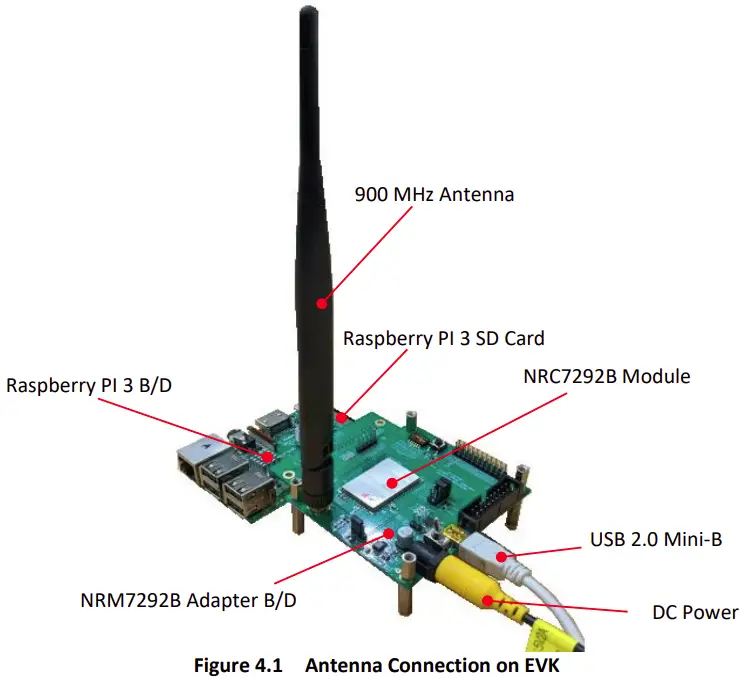
Operating Condition
Absolute Maximum Rating
Table 5.1 NRM7292D absolute maximum rating
Symbol | Min | Max | Unit | |
| Storage Temperature | -40 | +125 | ℃ | |
Supply Voltage | VDD_FEM | -0.5 | 5.25 | V |
| VBAT | -0.5 | 3.8 | V | |
VDDIO | -0.5 | 3.8 | V | |
- NOTE : Stresses above those listed in Absolute Maximum Rating may cause permanent device Functionality at or above these limits is not implied. Exposure to absolute maximum ratings for extended periods may affect device reliability.
Operating condition
Table 5.2 NRM7292D operating condition
Symbol | Min | Typ | Max | unit | |
| Operating Temperature Range | -40 | – | +85 | ℃ | |
Operating Voltage | VDD_FEM | 2.8 | 4.0 | 4.2 | V |
| VBAT | 2.8 | 3.3 | 3.6 | V | |
VDDIO | 1.8 | 3.3 | VBAT | V | |
- NOTE : To ensure WLAN performance, ripple on the 2.1- to 3.3-V supply must be less than ±300 mV and ripple on the 1.8-V supply must be less than 2% (±40 mV).
Current consumption
Table 5.3 NRM7292D current consumption
MODE | DUT Status | Band (MHz) | VDDIO (mA) | VBAT (mA) | VDD_FEM (mA) |
802.11ah (1/2/4Mhz BW) | Tx @ 17 dBm (VDD_FEM = 3.3V) | 915 | 0.5 | 33 | 148 |
| Tx @ 17 dBm (VDD_FEM = 4.0V) | 0.5 | 33 | 153 | ||
Tx @ 20 dBm (VDD_FEM = 3.3V) | 0.5 | 33 | 177 | ||
| Tx @ 20 dBm (VDD_FEM = 4.0V) | 0.5 | 33 | 184 | ||
Continuous Rx @ -80 dBm (VDD_FEM = 3.3V) | 0.5 | 33 | 7 | ||
| Continuous Rx @ -80 dBm (VDD_FEM = 4.0V) | 0.5 | 33 | 7 | ||
Deep Sleep mode | 0.6(uA) | 27(uA) | 0.4(uA) |
- Note: Unless otherwise specified, TA.=27℃, VBAT= 3.3V, 99% tx burst time, using internal PMU.
- Power measurements are done at antenna port, which is directly connected to the device.
- HSPI pins to host are disconnected.
11ah WLAN RF Specifications and Performance
Transmitter Specifications
Table 6.1 Transmitter Spec/Feature (RF)
Parameter | Conditions | Min | Typ | Max | Unit |
| RF Output Frequency Range (1) | 902 | 928 | MHz | ||
EVM Compliant Output Power | 15 Mbps (MCS7, 4 MHz BW) | 20 | dBm | ||
| EVM at 0 dBm output power | -35 | dB | |||
Transmitter Spurious Signal Emissions | < 700 MHz | <-36 | dBm/ MHz | ||
| > 1 GHz | <-45 | ||||
RF Output Return Loss | Single ended output port | -10 | dB | ||
| Output 1dB Gain Compression | 0.4 MHz CW signal input | 27 | dBm | ||
Gain Control Range | 30 | dB | |||
| Gain Control Step | 1 | dB | |||
Unwanted Sideband | Over RF channel, RF frequency, and baseband frequency at 0 dBm output power | <-40 | dBc |
- Note: Unless otherwise specified, TA.=27℃, VBAT=2.6 to 3.6V, VDD_FEM=4.0V. RF input/outputs specifications are referenced to device pins and do not include 1dB loss from EV kit OCB and SMA
(1) RF output frequency range depends on RF SAW filter on the module. The NRC7292 chipset by itself can support frequency range from 750 to 950 MHz.
Receiver Specifications
Table 6.2 Receiver Spec/Feature (RF)
Parameter | Conditions | Min | Typ | Max | Unit |
| RF Input Frequency Range (1) | 902 | 928 | MHz | ||
RF Input Return Loss | For LNA high/mid/low gain modes | -10 | -12 | -15 | dB |
| Total Voltage Gain Range | Analog + Digital Gain | -10 | 92 | dB | |
RF Gain Step | From high gain mode to medium gain mode | 6 | dB | ||
RX Gain Step | From RF to Analog | 1 | dB | ||
DSB Noise Figure | LNA max gain mode | 3.5 | dB | ||
IIP3 | LNA with high gain mode | -17 | dBm | ||
| LNA with low gain mode | 24 |
Baseband Filters for Receiver (Analog + Digital Filter) | |||||
| Baseband -3dB Low-pass Corner Frequency (Controllable) | 1 MHz channel | 0.5 | MHz | ||
| 2 MHz channel | 1.0 | MHz | |||
4 MHz channel | 2.0 | MHz | |||
- Note: Unless otherwise specified, TA.=27℃, VBAT=2.6 to 3.6V, VDD_FEM=4.0V. RF input/outputs specifications are referenced to device pins and do not include 1dB loss from EV kit OCB and SMA
(1) RF input frequency range depends on RF SAW filter on the module. The NRC7292 chipset by itself can support frequency range from 750 to 950 MHz.
Transmitter Performance
DR/MCS/BW (Mbps/ /MHz) | IEEE Relative constellation error (dB) | EVM (%) (IEEE) | EVM (%)(NRM7292D) | Comments |
0.15/MCS10/1 | -4 | 63.1 | 3.0 | BPSK Peak |
| 0.30/MCS0/1 | -5 | 56.2 | 3.0 | BPSK Peak |
0.60/MCS1/1 | -10 | 31.6 | 3.0 | 18 dBm OFDM, RMS |
| 0.90/MCS2/1 | -13 | 22.4 | 3.0 | 18 dBm OFDM, RMS |
1.20/MCS3/1 | -16 | 15.8 | 3.0 | 18 dBm OFDM, RMS |
| 1.80/MCS4/1 | -19 | 11.2 | 3.0 | 18 dBm OFDM, RMS |
2.40/MCS5/1 | -22 | 7.9 | 3.0 | 18 dBm OFDM, RMS |
| 2.70/MCS6/1 | -25 | 5.6 | 3.0 | 18 dBm OFDM, RMS |
3.00/MCS7/1 | -27 | 4.5 | 3.0 | 18 dBm OFDM, RMS |
| 0.65/MCS0/2 | -5 | 56.2 | 3.2 | BPSK Peak |
1.30/MCS1/2 | -10 | 31.6 | 3.2 | 18 dBm OFDM, RMS |
| 1.95/MCS2/2 | -13 | 22.4 | 3.2 | 18 dBm OFDM, RMS |
2.60/MCS3/2 | -16 | 15.8 | 3.2 | 18 dBm OFDM, RMS |
| 3.90/MCS4/2 | -19 | 11.2 | 3.2 | 18 dBm OFDM, RMS |
5.20/MCS5/2 | -22 | 7.9 | 3.2 | 18 dBm OFDM, RMS |
| 5.85/MCS6/2 | -25 | 5.6 | 3.2 | 18 dBm OFDM, RMS |
6.50/MCS7/2 | -27 | 4.5 | 3.2 | 18 dBm OFDM, RMS |
| 1.35/MCS0/4 | -5 | 56.2 | 3.0 | BPSK Peak |
2.70/MCS1/4 | -10 | 31.6 | 3.0 | 18 dBm OFDM, RMS |
| 4.05/MCS2/4 | -13 | 22.4 | 3.0 | 18 dBm OFDM, RMS |
5.40/MCS3/4 | -16 | 15.8 | 3.0 | 18 dBm OFDM, RMS |
| 8.10/MCS4/4 | -19 | 11.2 | 3.0 | 18 dBm OFDM, RMS |
10.80/MCS5/4 | -22 | 7.9 | 3.0 | 18 dBm OFDM, RMS |
| 12.15/MCS6/4 | -25 | 5.6 | 3.0 | 18 dBm OFDM, RMS |
13.50/MCS7/4 | -27 | 4.5 | 3.0 | 18 dBm OFDM, RMS |
- Conditions: supply voltage VBAT=2.6 ~ 3.6V, VDD_FEM=4.0V, Ta=25℃, signal within spectrum
Receiver Performance
Receiver Sensitivity
Table 6.4 Sensitivity (minimum input level)
Band | BW | Rate | Modulation/Coding Rate | Conditions | Chip Port Specification [dBm] | ||
| kbps | Min | Typ | Max | ||||
| 902~ 928MHz | 1 MHz | 300 | BPSK 1/2 | @ PER<10%, 256 bytes Full Operating Temperatures Battery Voltage Range; Load Z : 50 Ohms; | -106 | ||
| 600 | QPSK 1/2 | -104 | |||||
900 | QPSK 3/4 | -101 | |||||
| 1200 | 16QAM 1/2 | -98 | |||||
1800 | 16QAM 3/4 | -95 | |||||
| 2400 | 64QAM 2/3 | -91 | |||||
2700 | 64QAM 3/4 | -90 | |||||
| 3000 | 64QAM 5/6 | -88 | |||||
150 | BPSK 1/2 rep. 2x | -109 | |||||
| 2 MHz | 650 | BPSK 1/2 | @ PER<10%, 256 bytes Full Operating Temperature; Full Battery Voltage Range; Load Z : 50 Ohms; | -100 | |||
1300 | QPSK 1/2 | -98 | |||||
| 1950 | QPSK 3/4 | -97 | |||||
2600 | 16QAM 1/2 | -94 | |||||
| 3900 | 16QAM 3/4 | -91 | |||||
5200 | 64QAM 2/3 | -86 | |||||
| 5850 | 64QAM 3/4 | -85 | |||||
6500 | 64QAM 5/6 | -83 | |||||
| 4 MHz | 1350 | BPSK 1/2 | @ PER<10%, 256 bytes Full Operating Temperature; Full Battery Voltage Range; Load Z : 50 Ohms; | -99 | |||
2700 | QPSK 1/2 | -97 | |||||
| 4050 | QPSK 3/4 | -94 | |||||
5400 | 16QAM 1/2 | -91 | |||||
| 8100 | 16QAM 3/4 | -88 | |||||
10800 | 64QAM 2/3 | -83 | |||||
| 12150 | 64QAM 3/4 | -82 | |||||
13500 | 64QAM 5/6 | -80 | |||||
Adjacent Channel Rejection (ACR)
Band | BW | Rate | Modulation/Coding Rate | Conditions | ACR [dB] | ||
| kbps | Min | Typ | Max | ||||
| 902~ 928MHz | 1 MHz | 300 | BPSK 1/2 | @ PER<10%, Pdesired=Psensitivty + 3dB, Pinterfere]@ N+1 channel | 36 | ||
| 600 | QPSK 1/2 | 34 | |||||
900 | QPSK 3/4 | 31 | |||||
| 1200 | 16QAM 1/2 | 28 | |||||
1800 | 16QAM 3/4 | 26 | |||||
2400 | 64QAM 2/3 | 22 | |||||
| 2700 | 64QAM 3/4 | 20 | |||||
3000 | 64QAM 5/6 | 19 | |||||
| 150 | BPSK 1/2 rep. 2x | 39 | |||||
|
2 MHz | 650 | BPSK 1/2 | @ PER<10%, Pdesired=Psensitivty + 3dB, Pinterfere]@ N+1 channel | 32 | |||
| 1300 | QPSK 1/2 | 31 | |||||
1950 | QPSK 3/4 | 30 | |||||
2600 | 16QAM 1/2 | 27 | |||||
| 3900 | 16QAM 3/4 | 24 | |||||
5200 | 64QAM 2/3 | 21 | |||||
| 5850 | 64QAM 3/4 | 20 | |||||
6500 | 64QAM 5/6 | 19 | |||||
4 MHz | 1350 | BPSK 1/2 | @ PER<10%, Pdesired=Psensitivty + 3dB, Pinterfere]@ N+1 channel | 32 | |||
| 2700 | QPSK 1/2 | 29 | |||||
4050 | QPSK 3/4 | 28 | |||||
| 5400 | 16QAM 1/2 | 25 | |||||
| 8100 | 16QAM 3/4 | 22 | |||||
| 10800 | 64QAM 2/3 | 20 | |||||
12150 | 64QAM 3/4 | 17 | |||||
13500 | 64QAM 5/6 | 15 | |||||
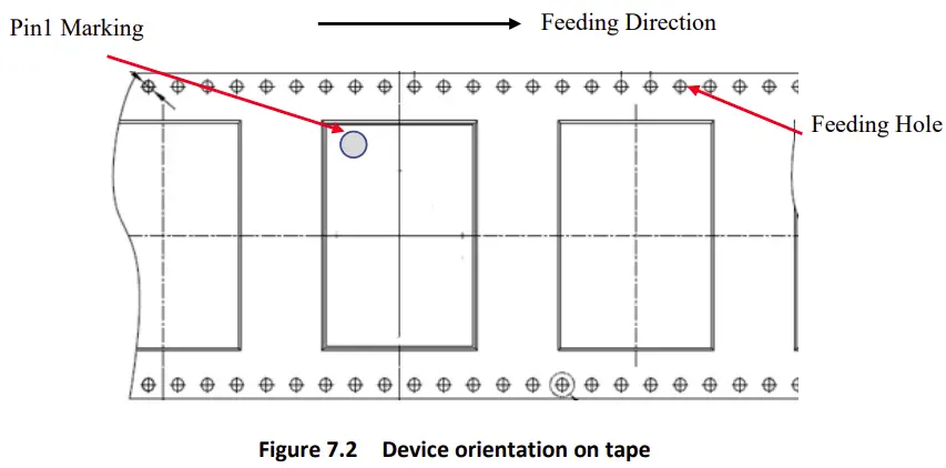
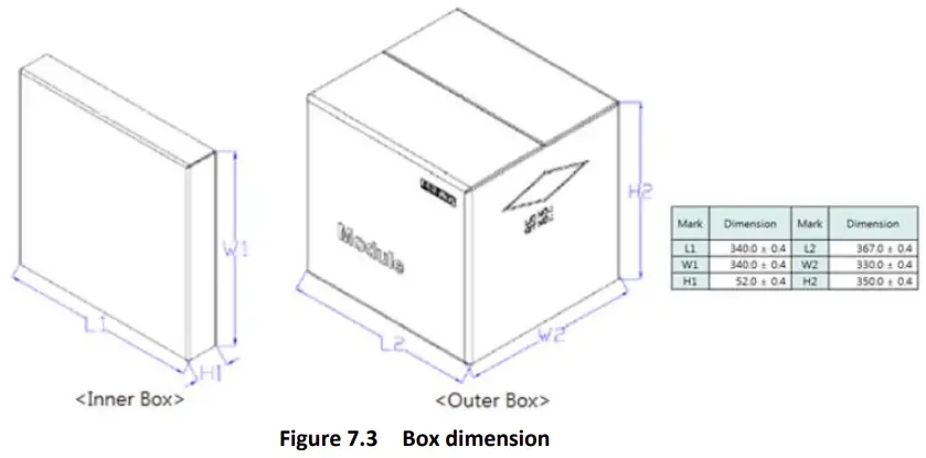
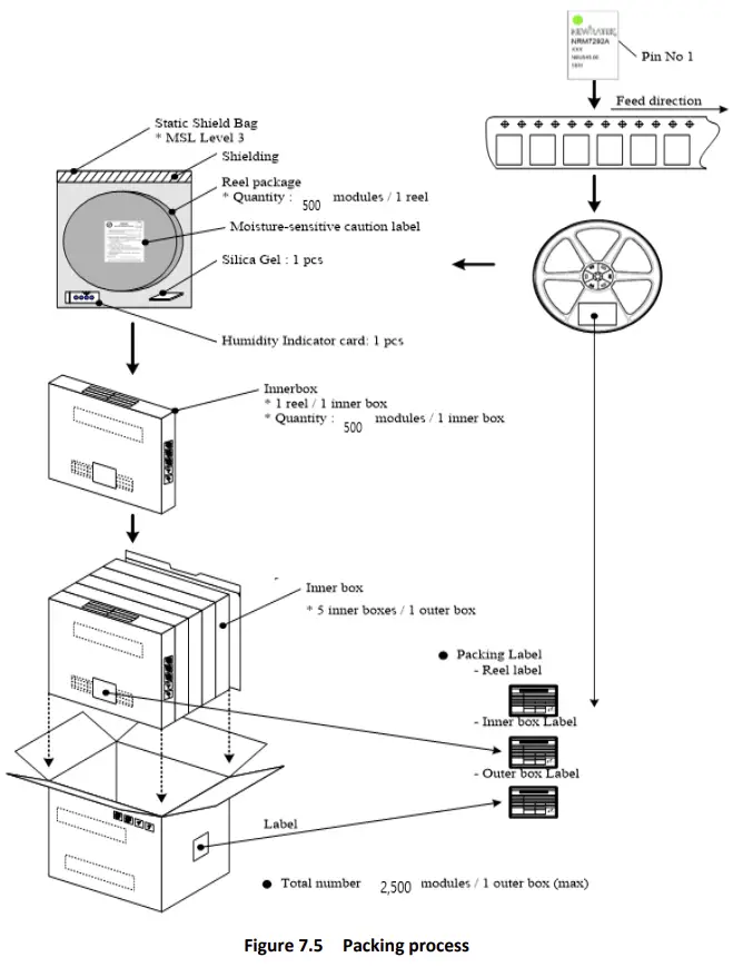
Packing Specification
Dimensions of Tape
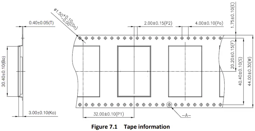
Taping Diagrams
Box Information
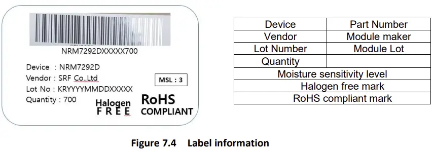
Label Information
- Reel / AL Bag / Inner Box
Packing Process
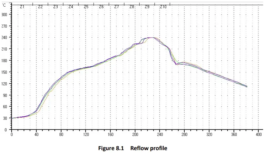
SMT Temperature Sequence (Pb-free)
Revision History
Revision No | Date | Comments |
| Ver 1.0 | 7/27/2022 | Initial version for customer release created |
FCC Compliance Statement
This device complies with part 15 of the FCC rules. Operation is subject to the following two conditions: (1) This device may not cause harmful interference, and (2) this device must accept any interference received, including interference that may cause undesired operation.
FCC Interference Statement
This equipment has been tested and found to comply with the limits for a Class B digital device, pursuant to part 15 of the FCC Rules. These limits are designed to provide reasonable protection against harmful interference in a residential installation. This equipment generates, uses and can radiate radio frequency energy and, if not installed and used in accordance with the instructions, may cause harmful interference to radio communications. However, there is no guarantee that interference will not occur in a particular installation. If this equipment does cause harmful interference to radio or television reception, which can be determined by turning the equipment off and on, the user is encouraged to correct the interference by one of the following measures:
- Reorient or relocate the receiving antenna.
- Increase the separation between the equipment and receiver.
- Connect the equipment into an outlet on a circuit different from which the receiver is connected.
- Consult the dealer or an experienced radio/TV technician for help
FCC Caution
Any changes or modifications not expressly approved by the party responsible for compliance could void the user’s authority to operate this equipment. This transmitter must not be co-located or operating in conjunction with any other antenna or transmitter.
FCC Radiation Exposure Statement
This equipment complies with FCC radiation exposure limits set forth for an uncontrolled environment. This equipment should be installed and operated with minimum distance 20 cm between the radiator and your body. This transmitter must not be co-located or operating in conjunction with any other antenna or transmitter.
Information on test modes and additional testing requirements
a) The modular transmitter has been fully tested by the module grantee on the required number of channels, modulation types and modes, it should not be necessary for the host installer to retest all the available transmitter modes or settings. It is recommended that the host product manufacturer installing the modular transmitter, perform some investigative measurements to confirm that the resulting composite system does not exceed the spurious emissions limits or band edge limits(e.g., where a different antenna may be causing additional emissions).
b) The testing should check for emissions that may occur due to the intermixing of emissions with the other transmitter, digital circuitry, or due to physical properties of the host product(enclosure).
This investigation is especially important when integrating multiple modular transmitters where the certification is based on testing each of them in a standalone configuration. It is important to note that host product manufactures should not assume that because the modular transmitter is certified that they do not have any responsibility for final product compliance.
Additional testing, Part 15 subpart B disclaimer
The final host/module combination need to be evaluated against the FCC Part 15B criteria for unintentional radiators in order to be properly authorized for operation as a Part 15 digital device.
The host integrator installing this module into their product must ensure that the final composite product complies with the FCC requirements by a technical assessment or evaluation to the FCC rules, including the transmitter operation and should refer to guidance in KDB 996369.
This appliance and its antenna must not be co-located or operation in conjunction with any other antenna or transmitter.
- OEM integrators must ensure that its product is electrically identical to the device, FCC ID: 2A32R-NRM7292D reference designs . Any modifications to module reference designs may invalidate regulatory approvals in relation to the product, or may necessitate notifications to the relevant regulatory authorities.
- OEM integrators are responsible for regression testing to accommodate changes to designs, new antennas, and host and submit for C2PC filings.
- Colocation with other transmitter modules will be addressed through filings for those co-located transmitters when necessary or that colocation of other transmitters will be according to applicable KDB guidelines including those for RF exposure
- Appropriate labels must be affixed to the product that complies with applicable regulations in all respects. The regulatory label on the final system must include the statement:
“Contains FCC ID: 2A32R-NRM7292D”.
- The module is limited to OEM installation ONLY.
- OEM integrators are responsible for ensuring that the end-user has no manual instructions to remove or install module.
- The module is limited to installation in mobile or fixed applications, according to Part 2.1091(b).
- Separate approval is required for all other operating configurations, including portable configurations with respect to Part 2.1093 and different antenna configurations.
End Product Labeling
The module is labeled with its own FCC ID. If the FCC ID is not visible when the module is installed inside another device, then the outside of the device into which the module is installed must also display a label referring to the enclosed module. In that case, the final end product must be labeled in a visible area with the following:
“Contains FCC ID: 2A32R-NRM7292D