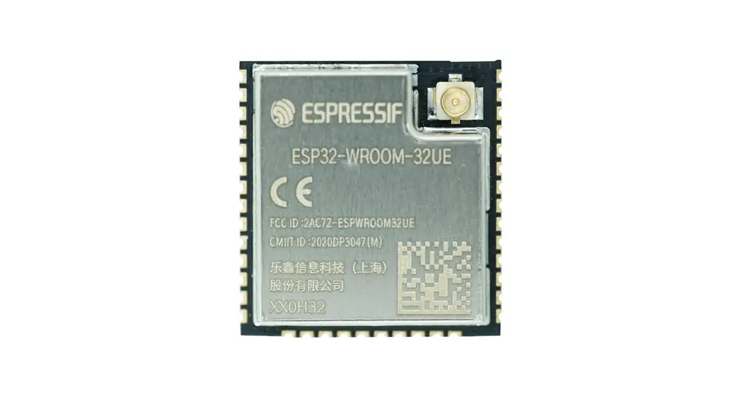
![]() ESP32-WROOM-32UE
ESP32-WROOM-32UE
User Manual
About This Document
This document provides the specifications for the ESP32-WROOM-32UE modules with PIFA antenna.
Overview
ESP32-WROOM-32UE is a powerful, generic WiFi-BT-BLE MCU module that targets a wide variety of applications, ranging from low-power sensor networks to the most demanding tasks, such as voice encoding, music streaming, and MP3 decoding.
It is with all GPIOs on the pin-out except the ones already used for connecting flash. The Module’s working voltage can range from 3.0 V to 3.6 V. Frequency range is 24
12 MHz to 24 62 MHz. External 40 MHz as the clock source for the system. There is also a 4 MB SPI flash for storing user programs and data. The ordering information of ESP32-WROOM-32UE is listed as follows:
Table 1: ESP32-WROOM-32UE Ordering Information
| Module | Chip embedded | Flash | PSRAM | Module dimensions (mm) |
| ESP32-WROOM-32UE | ESP32-D0WD-V3 | 4 MB 1 | / | (18.00 ± 0.10) X (25.50 ± 0.10) X (3.10 ± 0.10) mm (including metallic shield) |
| Notes: 1. ESP32-WROOM-32UE (IPEX) with 8 MB flash or 16 MB flash is available for a custom order. 2. For detailed ordering information, please see Espressif Product Ordering Information. | ||||
At the core of the module is the ESP32-D0WD-V3 chip*. The chip embedded is designed to be scalable and adaptive. There are two CPU cores that can be individually controlled, and the CPU clock frequency is adjustable from 80 MHz to 240 MHz. The user may also power off the CPU and make use of the low-power co-processor to constantly monitor the peripherals for changes or crossing of thresholds. ESP32 integrates a rich set of peripherals, ranging from capacitive touch sensors, Hall sensors, SD card interface, Ethernet, high-speed SPI, UART, I²S, and I²C.
Note:
* For details on the part numbers of the ESP32 family of chips, please refer to the document ESP32 User Manual.
The integration of Bluetooth, Bluetooth LE, and Wi-Fi ensures that a wide range of applications can be targeted and that the module is all-around: using Wi-Fi allows a large physical range and direct connection to the Internet through a Wi-Fi router while using Bluetooth allows the user to conveniently connect to the phone or broadcast low-energy beacons for its detection. The sleep current of the ESP32 chip is less than 5 A, making it suitable for battery-powered and wearable electronics applications. The module supports a data rate of up to 150 Mbps. As such the module does offer industry-leading specifications and the best performance for electronic integration, range, power consumption, and connectivity.
The operating system chosen for ESP32 is freeRTOS with LwIP; TLS 1.2 with hardware acceleration is built in as well. Secure (encrypted) over-the-air (OTA) upgrade is also supported, so that users can upgrade their products even after their release, at minimum cost and effort. Table 2 provides the specifications of ESP32-WROOM-32UE.
able 2: ESP32-WROOM-32UE Specifications
| Categories | Items | Specifications |
| Test | Reliablity | HTOUHTSUuHASTfTCT/ESD |
| Wi-Fi | Protocols | 802.11 b/g/n 20/n40 |
| A-MPDU and A-MSDU aggregation and 0.4 s guard interval support | ||
| Frequency range | 2.412 GHz – 2.462GHz | |
| Bluetooth | Protocols | Bluetooth v4.2 BR/EDR and BLE specification |
| Radio | NZIF receiver with -97 dBm sensitivity | |
| Class-1, class-2 and class-3 transmitter | ||
| AFH | ||
| AUCII0 | CVSD and SBC | |
| Hardware | Module interfaces | SD card, UART, SPI, SDIO, I2C, LED PWM, Motor PWN 12S, IR, pulse counter, GPIO, capacitive touch sensor, ADC, DAC |
| On-chip sensor | Hall sensor | |
| Integrated crystal | 40 MHz crystal | |
| Integrated SPI flash | 4 MB | |
| Integrated PSRAM | – | |
| Operating voltage/Power supply | 3.0 V – 3.6 V | |
| Minimum current delivered by the power supply | 500 mA | |
| Recommended operating temperature range 40 °C – 85 °C | ||
| Package size | (18.00±0.10) mm x (31.40±0.10) mm x (3.30±0.10) mm | |
| Moisture sensitivity level (MSL) | Level 3 |
Pin Definitions
2.1 Pin Layout
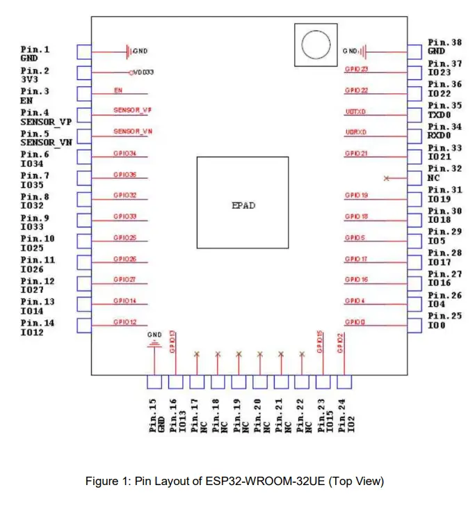
2.2 Pin Description
ESP32-WROOM-32UE has 38 pins. See pin definitions in Table 3.
Table 3: Pin Definitions
| Name | No. | Type | Function |
| GND | 1 | P | Ground |
| 3V3 | 2 | P | Power supply |
| EN | 3 | I | Module-enable signal. Active high. |
| SENSOR VP | 4 | I | GPI036, ADC1_CHO, RTC_GPIOO |
| SENSOR VN | 5 | I | GPI039, ADC1 CH3, RTC GP103 |
| 1034 | 6 | I | GPI034, ADC1_CH6, RTC_GPIO4 |
| 1035 | 7 | 1 | GPI035, ADC1_CH7, RTC_GPIO5 |
| 1032 | 8 | I/O | GPI032, XTAL 32K P (32.768 kHz crystal oscillator input), ADC1_CH4 TOUCH9, RTC GP109 |
| 1033 | 9 | 1/0 | GPI033, XTAL_32K_N (32.768 kHz crystal oscillator output), ADC1 CH5, TOUCH8, RTC GP108 |
| 1025 | 10 | I/O | GPIO25, DAC_1, ADC2_CH8, RTC_GPIO6, EMAC_RXDO |
| 1026 | 11 | 1/0 | GPIO26, DAC_2, ADC2_CH9, RTC_GPIO7, EMAC_RXD1 |
| 1027 | 12 | 1/0 | GPIO27, ADC2_CH7, TOUCH7, RTC_GPI017, EMAC_RX_DV |
| 1014 | 13 | I/O | GPIO14, ADC2 CH6, TOUCH6, RTC GPIO16, MTMS, HSPICLK, HS2_CLK, SD_CLK, EMAC_TXD2 |
| 1012 | 14 | I/O | GPI012, ADC2_CH5, TOUCH5, RTC GPIO15, MTDI, HSPIQ, HS2_DATA2, SD_DATA2, EMAC_TXD3 |
| GND | 15 | P | Ground |
| 1013 | 16 | I/O | GPI013, ADC2 CH4, TOUCH4, RTC GPI014, MTCK, HSPID, HS2_DATA3, SD_DATA3, EMAC_RX_ER |
| NC | 17 | – | – |
| NC | 18 | – | – |
| NC | 19 | – | – |
| NC | 20 | – | – |
| NC | 21 | – | – |
| NC | 22 | – | – |
| 1015 | 23 | I/O | GPIO15, ADC2 CH3, TOUCH3, MTDO, HSPICSO, RTC GPI013, HS2_CMD, SD_CMD, EMAC_RXD3 |
| 102 | 24 | 1/0 | GPIO2, ADC2_CH2, TOUCH2, RTC GPI012, HSPIWP, HS2_DATAO, SD DATA() |
| 100 | 25 | I/O | GPIOO, ADC2_CH1, TOUCH1, RTC_GPIO11, CLK_OUT1, IMAC TX CLK _ _ |
| 104 | 26 | I/O | GPIO4, ADC2_CHO, TOUCH, RTC_GPI010, HSPIHD, HS2_DATA1, SD DATA1, EMAC_TX_ER |
| 1016 | 27 | 1/0 | GPIOI6, ADC2_CH8, TOUCH |
| 1017 | 28 | 1/0 | GPI017, ADC2_CH9, TOUCH11 |
| 105 | 29 | 1/0 | GPIO5, VSPICSO, HS1_DATA6, EMAC_RX_CLK |
| 1018 | 30 | 1/0 | GPI018, VSPICLK, HS1_DATA7 |
| Name | No. | Type | Function |
| 1019 | 31 | I/O | GPIO19, VSPIQ, UOCTS, EMAC_TXDO |
| NC | 32 | – | – |
| 1021 | 33 | I/O | GPIO21, VSPIHD, EMAC_TX_EN |
| RXDO | 34 | I/O | GPIO3, UORXD, CLK_OUT2 |
| TXDO | 35 | I/O | GPIO1, UOTXD, CLK_OUT3, EMAC_RXD2 |
| 1022 | 36 | I/O | GPIO22, VSPIWP, UORTS, EMAC_TXD1 |
| 1023 | 37 | I/O | GPIO23, VSPID, HS1_STROBE |
| GND | 38 | P | Ground |
Notice:
* GPIO6 to GPIO11 are connected to the SPI flash integrated on the module and are not connected out.
2.3 Strapping Pins
ESP32 has five strapping pins, which can be seen in Chapter 6 Schematics:
- MTDI
- GPIO0
- GPIO2
- MTDO
- GPIO5
The software can read the values of these five bits from the register ”GPIO_STRAPPING”. During the chip’s system reset release (power-on-reset, RTC watchdog reset, and brownout reset), the latches of the strapping pins sample the voltage level as strapping bits of ”0” or ”1”, and hold these bits until the chip is powered down or shut down. The strapping bits configure the device’s boot mode, the operating voltage of VDD_SDIO, and other initial system settings.
Each strapping pin is connected to its internal pull-up/pull-down during the chip reset. Consequently, if a strapping pin is unconnected or the connected external circuit is high-impedance, the internal weak pull-up/pull-down will determine the default input level of the strapping pins.
To change the strapping bit values, users can apply the external pull-down/pull-up resistances, or use the host MCU’s GPIOs to control the voltage level of these pins when powering on ESP32. After reset release, the strapping pins work as normal-function pins. Refer to Table 4 for a detailed boot-mode configuration by strapping pins.
Table 4: Strapping Pins
| Voltage of Internal LDO (VDD_SDIO) | |||
| Pin | Default | 3.3 V | 1.8 V |
| MTDI | Pull-down | 0 | 1 |
| Booting Mode | ||||
| Pin | Default SPI Boot | Download Boot | ||
| GPIOO | Pull-up 1 | 0 | ||
| GPIO2 | Pull-down Don’t-care | 0 | ||
| Enabling/Disabling Debugging Log Print over UOTXD During Booting | ||||
| Pin | Default UOTXD Active | UOTXD Silent | ||
| MTDO | Pull-up 1 | 0 | ||
| Timing of SDIO Slave | ||||
| Pin | Falling-edge Sampling Default Falling-edge Output | Falling-edge Sampling Rising-edge Output | Rising-edge Sampling Falling-edge Output | Rising-edge Sampling Rising-edge Output |
| MTDO | Pull-up 0 | 0 | 1 | 1 |
| GPIO5 | Pull-up 0 | 1 | 0 | 1 |
Note:
- Firmware can configure register bits to change the settings of ”Voltage of Internal LDO (VDD_SDIO)” and ”Timing of SDIO Slave” after booting.
- Internal pull-up resistor (R9) for MTDI is not populated in the module, as the flash and SRAM in ESP32- WROOM-32UE only support a power voltage of 3.3 V (output by VDD_SDIO)
Functional Description
This chapter describes the modules and functions integrated with ESP32-WROOM-32UE.
3.1 CPU and Internal Memory
ESP32-D0WD-V3 contains two low-power Xtensa® 32-bit LX6 microprocessors. The internal memory includes:
- 448 KB of ROM for booting and core functions.
- 520 KB of on-chip SRAM for data and instructions.
- 8 KB of SRAM in RTC, which is called RTC FAST Memory and can be used for data storage; it is accessed by the main CPU during RTC Boot from the Deep-sleep mode.
- 8 KB of SRAM in RTC, which is called RTC SLOW Memory and can be accessed by the co-processor during the Deep-sleep mode.
- 1 Kbit of eFuse: 256 bits are used for the system (MAC address and chip configuration) and the remaining 768 bits are reserved for customer applications, including flash encryption and chip-ID.
3.2 External Flash and SRAM
ESP32 supports multiple external QSPI flash and SRAM chips. More details can be found in Chapter SPI in the ESP32 Technical Reference Manual. ESP32 also supports hardware encryption/decryption based on AES to protect developers’ programs and data in flash.
ESP32 can access the external QSPI flash and SRAM through high-speed caches.
- The external flash can be mapped into CPU instruction memory space and read-only memory space simultaneously.
– When the external flash is mapped into CPU instruction memory space, up to 11 MB + 248 KB can be mapped at a time. Note that if more than 3 MB + 248 KB are mapped, cache performance will be reduced due to speculative reads by the CPU.
– When an external flash is mapped into read-only data memory space, up to 4 MB can be mapped at a time. 8-bit, 16-bit, and 32-bit reads are supported. - External SRAM can be mapped into CPU data memory space. Up to 4 MB can be mapped at a time. 8- bit, 16-bit, and 32-bit read and writes are supported.
ESP32-WROOM-32UE integrates a 4 MB SPI flash more memory space.
3.3 Crystal Oscillators
The module uses a 40-MHz crystal oscillator.
3.4 RTC and Low-Power Management
With the use of advanced power-management technologies, ESP32 can switch between different power modes. For details on ESP32’s power consumption in different power modes, please refer to section ”RTC and Low-Power Management” in ESP32 User Manual.
Peripherals and Sensors
Please refer to Section Peripherals and Sensors in the ESP32 User Manual.
Note:
External connections can be made to any GPIO except for GPIOs in the range 6-11, 16, or 17. GPIOs 6-11 are connected to the module’s integrated SPI flash. For details, please see Section 6 Schematics.
Electrical Characteristics
5.1 Absolute Maximum Ratings
Stresses beyond the absolute maximum ratings listed in the table below may cause permanent damage to the device. These are stress ratings only, and do not refer to the functional operation of the device that should follow the recommended operating conditions.
Table 5: Absolute Maximum Ratings
- The module worked properly after a 24-hour test in ambient temperature at 25 °C, and the IOs in three domains (VDD3P3_RTC, VDD3P3_CPU, VDD_SDIO) output high logic level to the ground. Please note that pins occupied by flash and/or PSRAM in the VDD_SDIO power domain were excluded from the test.
- Please see Appendix IO_MUX of ESP32 User Manual for IO’s power domain.
5.2 Recommended Operating Conditions
Table 6: Recommended Operating Conditions
| Symbol | Parameter | Min | Typical | Max | Unit |
| VDD33 | Power supply voltage | 3.0 | 3. | 4. | V |
| ‘V | Current delivered by the external power supply | 0.5 | – | – | A |
| T | Operating temperature | —40 | – | 85 | °C |
5.3 DC Characteristics (3.3 V, 25 °C)
Table 7: DC Characteristics (3.3 V, 25 °C)
| Symbol | Parameter | Min | Typ | Max | Unit | |
| L. IN | Pin capacitance | 2 | – | pF | ||
| V IH | High-level input voltage | 0.75XVDD1 | _ | VDD1+0.3 | v | |
| v IL | Low-level input voltage | —0.3 | – | 0.25xVDD1 | V | |
| i IH | High-level input current | – | – | 50 | nA | |
| i IL | Low-level input current | – | 50 | nA | ||
| V OH | High-level output voltage | 0.8XVDD1 | V | |||
| VOA | Low-level output voltage | – | V | |||
| 1 OH | High-level source current (VDD1 = 3.3 V, VOH >= 2.64V, output drive strength set to the maximum) | VDD3P3 CPU power domain 1; 2 | _ | 40 | – | mA |
| VDD3P3 RTC power domain 1; 2 | _ | 40 | – | mA | ||
| VDD SDIO power domain 1; 3 | – | 20 | – | mA | ||
| Symbol | Parameter | Min | Typ | Max | Unit |
| 10L | Low-level sink current (VDD1 = 3.3 V, VOL = 0.495 V, output drive strength set to the maximum) | – | 28 | mA | |
| RP u | Resistance of internal pull-up resistor | – | 45 | – | kil |
| P D | Resistance of internal pull-down resistor | – | 45 | – | kil |
| V IL_nRST | Low-level input voltage of CHIP_PU to power off the chip | – | – | 0.6 | V |
Notes:
- Please see Appendix IO_MUX of ESP32 User Manual for IO’s power domain. VDD is the I/O voltage for a particular power domain of pins.
- For VDD3P3_CPU and VDD3P3_RTC power domain, per-pin current sourced in the same domain is gradually reduced from around 40 mA to around 29 mA, VOH>=2.64 V, as the number of current-source pins increases.
- Pins occupied by flash and/or PSRAM in the VDD_SDIO power domain were excluded from the test.
5.4 Wi-Fi Radio
Table 8: Wi-Fi Radio Characteristics
| Parameter | Condition | Min | Typical | Max | Unit | ||
| Operating frequency range notes | 2412 | – | 2462 | MHz | |||
| Output impedance note2 | * | C2 | |||||
| TX power note3 | 802.1 1 b:24.16dBm:802.11g:23.52dBm 802.11n20:23.0IdBm;802.1 I n40:21.18d13m dBm | ||||||
| Sensitivity | 11b, 1 Mbps | – | —98 | dBm | |||
| 11b, 11 Mbps | – | —89 | dBm | ||||
| 11g, 6 Mbps | —92 | – | dBm | ||||
| 11g, 54 Mbps | —74 | – | dBm | ||||
| 11n, HT20, MCSO | —91 | – | dBm | ||||
| 11n, HT20, MCS7 | —71 | dBm | |||||
| 11n, HT40, MCSO | —89 | dBm | |||||
| 11n, HT40, MCS7 | —69 | dBm | |||||
| Adjacent channel rejection | 11g, 6 Mbps | 31 | – | dB | |||
| 11g, 54 Mbps | 14 | dB | |||||
| 11n, HT20, MCSO | 31 | dB | |||||
| 11n, HT20, MCS7 | – | 13 | dB | ||||
- Device should operate in the frequency range allocated by regional regulatory authorities. Target operating frequency range is configurable by software.
- For the modules that use IPEX antennas, the output impedance is 50 Ω. For other modules without IPEX antennas, users do not need to be concerned about the output impedance.
- Target TX power is configurable based on device or certification requirements.
5.5 Bluetooth/BLE Radio
5.5.1 Receiver
Table 9: Receiver Characteristics – Bluetooth/BLE
| Parameter | Conditions | Min | Typ | Max | Unit |
| Sensitivity @30.8% PER | -97 | – | dBm | ||
| Maximum received signal @30.8% PER | – | 0 | – | – | dBm |
| Co-channel C/I | – | – | +10 | – | dB |
| Adjacent channel selectivity C/I | F = FO + 1 MHz | – | -5 | – | dB |
| F = FO – 1 MHz | – | -5 | dB | ||
| F = FO + 2 MHz | – | -25 | – | dB | |
| F = FO – 2 MHz | – | -35 | – | dB | |
| F = FO + 3 MHz | – | -25 | – | dB | |
| F = FO – 3 MHz | – | -45 | – | dB | |
| Out-of-band blocking performance | 30 MHz – 2000 MHz | -10 | – | – | dBm |
| 2000 MHz – 2400 MHz dBm | -27 | – | – | ||
| 2500 MHz – 3000 MHz | -27 | – | – | dBm | |
| 3000 MHz – 12.5 GHz | -10 | – | – | dBm | |
| itiudulatitm 1 | – | -36 | – | – | dBm |
5.5.2 Transmitter
Table 10: Transmitter Characteristics – Bluetooth/BLE
| Parameter | Conditions | Min | Typ | Max | Unit | |
| Gain control step | 3 | dBm | ||||
| RF power | – | BT3.0:7.73dBm BLE:4.92dBm | dBm | |||
| Adjacent channel transmits power | F = FO ± 2 MHz | – | —52 | – | dBm | |
| F = FO ± 3 MHz | – | —58 | – | dBm | ||
| F = FO ± > 3 MHz | —60 | – | dBm | |||
| A flaw | – | – | 265 | kHz | ||
| a fzmax | 247 | – | kHz | |||
| An f2avq/A f1avg | – | —0.92 | – | – | ||
| 1CFT | – | —10 | – | kHz | ||
| Drift rate | 0.7 | – | kHz/50 s | |||
| Drift | – | 2 | – | kHz | ||
5.6 Reflow Profile
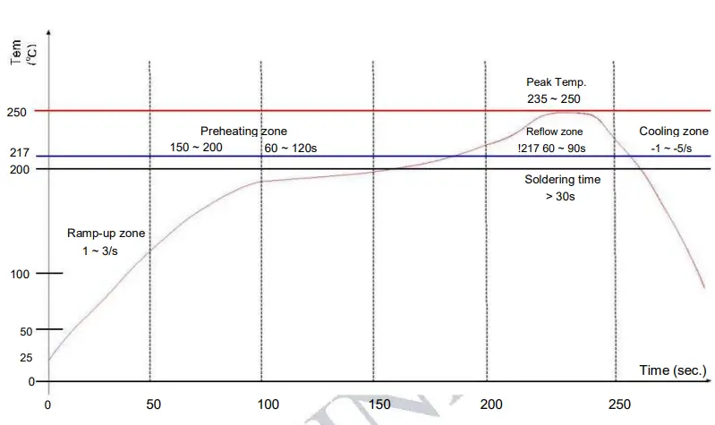
Ramp-up zone — Temp.: <150 Time: 60 ~ 90s Ramp-up rate: 1 ~ 3/s
Preheating zone — Temp.: 150 ~ 200 Time: 60 ~ 120s Ramp-up rate: 0.3 ~ 0.8/s
Reflow zone — Temp.: >217 7LPH60 ~ 90s; Peak Temp.: 235 ~ 250 (<245 recommended) Time: 30 ~ 70s
Cooling zone — Peak Temp. ~ 180 Ramp-down rate: -1 ~ -5/s
Solder — Sn&Ag&Cu Lead-free solder (SAC305)
Revision History
| Date | Version | Release notes |
| 2020.02 | V0.1 | Preliminary release for certification CE. |
OEM Guidance
- Applicable FCC rules
This module is granted Single Modular Approval. It complies with the requirements of FCC part 15C, section 15.247 rules. - The specific operational use conditions
This module can be used in RF devices. The input voltage to the module is nominally 3. 0V-3.6 V DC. The operational ambient temperature of the module is – 40 to 85 degrees C. - Limited module procedures
N/A - Trace antenna design
N/A - RF exposure considerations
The equipment complies with FCC radiation exposure limits set forth for an uncontrolled environment. This equipment should be installed and operated with a minimum distance of 20cm between the radiator and your body. If the equipment is built into a host for portable usage, the additional RF exposure evaluation may be required as specified by 2.1093. - Antenna
Antenna type: PIFA antenna with IPEX connector; Peak gain: 4dBi - Label and compliance information
An exterior label on OEM’s end product can use wording such as the following:
“Contains FCC ID: 2AC7Z-ESPWROOM32UE” and
“Contains IC: 21098-ESPWROOMUE” - Information on test modes and additional testing requirements
a)The modular transmitter has been fully tested by the module grantee on the required number of channels, modulation types, and modes, it should not be necessary for the host installer to re-test all the available transmitter modes or settings. It is recommended that the host product manufacturer, install the modular transmitter, and perform some investigative measurements to confirm that the resulting composite system does not exceed the spurious emissions limits or band edge limits (e.g., where a different antenna may be causing additional emissions).
b)The testing should check for emissions that may occur due to the intermixing of emissions with the other transmitters, digital circuitry, or due to physical properties of the host product (enclosure). This investigation is especially important when integrating multiple modular transmitters where the certification is based on testing each of them in a stand-alone configuration. It is important to note that host product manufacturers should not assume that because the modular transmitter is certified that they do not have any responsibility for final product compliance.
c)If the investigation indicates a compliance concern the host product manufacturer is obligated to mitigate the issue. Host products using a modular transmitter are subject to all the applicable individual technical rules as well as to the general conditions of operation in Sections 15.5, 15.15, and 15.29 to not cause interference. The operator of the host product will be obligated to stop operating the device until the interference has been corrected. - Additional testing, Part 15 Subpart B disclaimer The final host/module combination needs to be evaluated against the FCC Part 15B criteria for unintentional radiators in order to be properly authorized for operation as a Part 15 digital device. The host integrator installing this module into their product must ensure that the final
composite product complies with the FCC requirements by a technical assessment or evaluation of the FCC rules, including the transmitter operation, and should refer to the guidance in KDB 996369. For host products with a certified modular transmitter, the frequency range of investigation of the composite system is specified by rule in Sections 15.33(a)(1) through (a)(3), or the range applicable to the digital device, as shown in Section 15.33(b)(1), whichever is the higher frequency range of investigation When testing the host product, all the transmitters must be operating. The transmitters can be enabled by using publicly- available drivers and turned on, so the transmitters are active. In certain conditions, it might be appropriate to use a technology-specific call box (test set) where accessory 50 devices or drivers are not available. When testing for emissions from the unintentional radiator, the transmitter shall be placed in the receive mode or idle mode, if possible. If receive mode only is not possible then, the radio shall be passive (preferred) and/or active scanning. In these cases, this would need to enable activity on the communication BUS (i.e., PCIe, SDIO, USB) to ensure the unintentional radiator circuitry is enabled. Testing laboratories may need to add attenuation or filters depending on the signal strength of any active beacons (if applicable)
from the enabled radio(s). See ANSI C63.4, ANSI C63.10, and ANSI C63.26 for further general testing details.
The product under test is set into a line association with a partnering device, as per the normal intended use of the product. To ease testing, the product under test is set to transmit at a high duty cycle, such as by sending a file or streaming some media content.
FCC statement
This device complies with Part 15 of the FCC Rules. Operation is subject to the following two conditions:
(1) this device may not cause harmful interference, and (2) this device must accept any interference
(2) received, including interference that may cause undesired operation.
FCC Caution:
Any changes or modifications not expressly approved by the party responsible for compliance could void the user’s authority to operate the equipment.
“This equipment has been tested and found to comply with the limits for a Class B digital device,
pursuant to part 15 of the FCC Rules. These limits are designed to protect reasonably against harmful interference in a residential installation. This equipment generates, uses, and can radiate radio frequency energy and, if not installed and used in accordance with the instructions, may cause harmful interference to radio communications. However, there is no guarantee that interference will not occur in a particular installation. If this equipment does cause harmful interference to radio or television reception, which can be determined by turning the equipment off and on, the user is encouraged to try to correct the interference by one or more of the following measures:
- Reorient or relocate the receiving antenna.
- Increase the separation between the equipment and receiver.
- Connect the equipment into an outlet on a circuit different from that to which the receiver is connected.
- Consult the dealer or an experienced radio/TV technician for help.”
IC statement:
This device complies with Industry Canada licence-exempt RSS standard(s). Operation is subject to the following two conditions: (1) this device may not cause interference,
and (2) this device must accept any interference, including interference that may cause undesired operation of the device.


