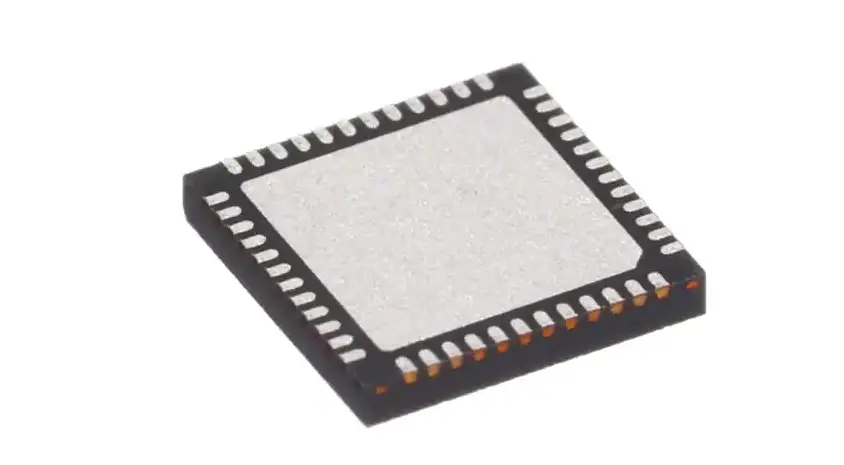
HANSONG HSBT3007-IA Full-Speed (12 Mbps) USB Interface Bluetooth Module
HANSONG (NANJING) TECHNOLOGY CO. , LTD.
| APROVED | MANAGER | CHECKED | FILLED |
Costumer
| S.MANAGER | MANAGER | CHECKED | CHIEF | FILLED |
Revision control
| Revision | Date/Author | Check by | Approve by | Remarks |
| V1.0 | Bruce/6.08.2020 | |||
| V2.0 | Bruce/7.13.2020 | Add FCC Statement | ||
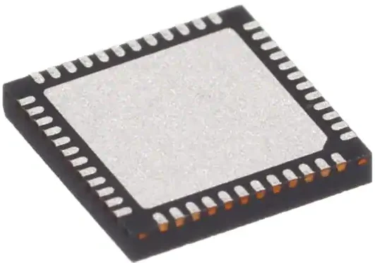
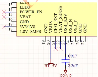
Pin view
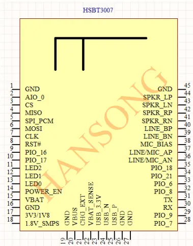
Pin Assignment
| Terminal | Pin Name | Pin Type | Description |
| 1. | GND | GND | Common Ground |
| 2. | AIO_0 | Bidirectional | Analog programmable input line 0 |
| 3. | CS | Bidirectional with weak pull-down | Programmable input/output line 4. Alternative function: ■ SPI_CS#: chip select for Debug SPI, active low ■ I2S1_WS: I2S1 word select |
| 4. | MISO | Bidirectional with weak pull-down | Programmable input/output line 3. Alternative function: ■ SPI_MISO: Debug SPI data output ■ I2S1_SD_OUT: I2S1 synchronous data output |
| 5. | SPI_PCM | Input with weak pulldown | SPI/I2S select input: ■ 0 = I2S/PIO interface ■ 1 = SPI |
| 6. | MOSI | Bidirectional with weak pull-down | Programmable input/output line 2. Alternative function: ■ SPI_MOSI: Debug SPI data input ■ I2S1_SD_IN: I2S1 synchronous data input ■ SPDIF_IN: SPDIF input |
| 7. | CLK | Bidirectional with weak pull-down | Programmable input/output line 5. Alternative function: ■ SPI_CLK: Debug SPI clock ■ I2S1_SCK: I2S1 synchronous data clock |
| 8. | RST# | Input with strong pull-up | Reset if low. Pull low for minimum 5 ms to cause a reset. |
| 9. | PIO_16 | Bidirectional with strong pull-up | Programmable input/output line 16. Alternative function: ■ UART_RTS: UART request to send, active low |
| 10. | PIO_17 | Bidirectional with strong pull-down | Programmable input/output line 17. Alternative function: ■ UART_CTS: UART clear to send, active low |
| 11. | LED2 | Bidirectional | Open-drain output |
| 12. | LED1 | Bidirectional | Open-drain output |
| 13. | LED0 | Bidirectional | Open-drain output |
| 14. | POWER_EN | input | A high input (tolerant to VBAT voltages) |
| enables the on-chip regulators | |||
| 15. | VBAT | Power in | VBAT 3.3V—4.2V |
| 16. | GND | ||
| 17. | 3V3/1V8 | Power in | 3V3/1V8 TO Flash and IO VDD |
| 18. | 1.8V_SMPS | Power out | 1.8V_SMPS out |
| 19. | GND | GND | Common Ground |
| 20. | VBUS | Power in | Charger input. Typically connected to USB VBUS. |
| 21. | CHG_EXT | output | External battery charger transistor base control when using external charger boost. Otherwise leave unconnected. |
| 22. | VBAT_SENSE | input | Battery charger sense input. |
| 23. | USB_3.3V | Power out | USB_3.3V OUT |
| 24. | USB_N | Bidirectional | USB data N |
| 25. | USB_P | Bidirectional | USB data P |
| 26. | GND | GND | Common Ground |
| 27. | GND | GND | Common Ground |
| 28. | PIO_7 | Bidirectional | Programmable input/output line 7. |
| with | Alternative function: | ||
| strong | ■ I2S2_WS: I2S2 word select | ||
| pull-down | |||
| 29. | PIO_9 | Bidirectional | Programmable input/output line 9. |
| with | Alternative function: | ||
| strong | ■ UART_CTS: UART clear to send, active | ||
| pull-down | low | ||
| ■ I2S2_SCK: I2S2 synchronous data clock | |||
| 30. | RX | Bidirectional | Programmable input/output line 0. |
| with | Alternative function: | ||
| strong | ■ UART_RX: UART data input | ||
| pull-up | |||
| 31. | TX | Bidirectional | Programmable input/output line 1. |
| with | Alternative function: | ||
| strong | ■ UART_TX: UART data output | ||
| pull-up | |||
| 32. | PIO_8 | Bidirectional | Programmable input/output line 8. |
| with | Alternative function: | ||
| strong | ■ UART_RTS: UART request to send, active | ||
| pull-up | low | ||
| ■ I2S2_SD_IN: I2S2 synchronous data input | |||
| 33. | PIO_6 | Bidirectional | Programmable input/output line 6. |
| with | Alternative function: | ||
| strong | ■ I2S2_SD_OUT: I2S2 synchronous data | ||
| pull-down | output |
| 34. | PIO_21 | Bidirectional with weak pull-down | Programmable input/output line 21. |
| 35. | PIO_18 | Bidirectional with weak pull-down | Programmable input/output line 18. |
| 36. | LINE/MIC_AN | Analog in | Line or microphone input negative, channel A |
| 37. | LINE/MIC_AP | Analog in | Line or microphone input positive, channel A |
| 38. | MIC_BIAS | Analog in | Microphone bias |
| 39 | LINE_BN | Analog in | Line input negative, channel B |
| 40 | LINE_BP | Analog in | Line input positive, channel B |
| 41 | SPKR_RN | Analog out | Speaker output negative, right |
| 42 | SPKR_RP | Analog out | Speaker output positive, right |
| 43 | SPKR_LN | Analog out | Speaker output negative, left |
| 44 | SPKR_LP | Analog out | Speaker output positive, left |
| 45 | GND | GND | Common Ground |
Interfaces
USB Interface
HSBT3007 has a full-speed (12 Mbps) USB interface for communicating with other compatible digital devices.
The USB interface on HSBT3007 acts as a USB peripheral, responding to requests from a master host controller.
HSBT3007 contains internal USB termination resistors and requires no external resistors. HSBT3007 supports the Universal Serial Bus Specification, Revision v2.0 (USB v2.0 Specification), supports USB standard charger detection, and fully supports the USB Battery Charging Specification v1.2.
As well as describing USB basics and architecture, the application note describes:
- Power distribution for high and low bus-powered configurations
- Power distribution for self-powered configuration, which includes USB VBUS monitoring
- USB enumeration
- Electrical design guidelines for the power supply and data lines, as well as PCB tracks and the effects of ferrite beads
- USB suspend support
- Battery charging from USB, which describes dead battery provision, charge currents,charging in suspend modes, and USB VBUS voltage consideration
- USB termination when interface is not in use
- Internal modules, certification, and non-specification compliant operation
UART Interface
HSBT3007 has a UART serial interface that provides a simple mechanism for communicating with other serial devices using the RS232 protocol, including for test and debug. The UART interface is multiplexed with PIOs and other functions, and hardware flow control is optional. When HSBT3007 is connected to another digital device, UART_RX and UART_TX transfer data between the 2 devices. The remaining 2 signals, UART_CTS and UART_RTS, implement optional RS232 hardware flow control where both are active low indicators.
UART configuration parameters, such as baud rate and packet format, are set using the HSBT3007 firmware.
3.3 SPI Interface
HSBT3007 provides a debug SPI interface for programming, configuring (PS Keys) and debugging the HSBT3007. Access to this interface is required in production. Ensure the 4 SPI signals and the SPI/PCM# line are brought out to either test points or a header. To use the SPI interface, the SPI/PCM# line requires the option of being pulled high externally.
I2C Interface
The HSBT3007 supports an I2C interface for I/O port expansion. The default assignment of the I2C interface onto the PIOs on the HSBT3007 is:
- PIO[0] is the I2C interface SCL line (AMP_I2C_SCL)
- PIO[1] is the I2C interface SDA line (AMP_I2C_SDA)
Alternatively, the I2C interface can be assigned to two PIOs from PIO[9:0] using PSKEY_I2C_SCL_PIO and PSKEY_I2C_SDA_PIO.
NOTE The I2C interface requires external pull-up resistors. Ensure that external pull-up resistors are suitably sized for the I2C interface speed and PCB track capacitance.
LED Drivers
HSBT3007 includes a 3-pad PWM LED driver for driving RGB LEDs for producing a wide range of colors. All LEDs are controlled by application. The terminals are open-drain outputs, so the LED must be connected from a positive supply rail to the pad in series with a current-limiting resistor.
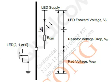
From Figure 7-1 it is possible to derive Equation 7-1 to calculate ILED. If a known value of current is required through the LED to give a specific luminous intensity, then the value of RLED is calculated.
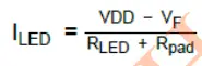
Equation 7-1 LED current
NOTE The supply domain for LED[2:0], VDD_PADS_2, or VDD_PADS_1, must remain powered for LED functions to operate.
Audio interfaces
- Dual I²S outputs
- I²S input, SPDIF input (uncompressed PCM only)
- USB audio
- Stereo audio ADC with line input, stereo audio DAC
- Supported sample rates of 8, 11.025, 16, 22.05, 32, 44.1, and 48kHz
Reset
HSBT3007 is reset from several sources:
- RST# pin
- Power-on reset
- USB charger attach reset
- Software configured watchdog timer
The RST# pin is an active low reset and is internally filtered using the internal low frequency clock oscillator. Recommends applying RST# for a period >5ms.
At reset the digital I/O pins are set to inputs for bidirectional pins and outputs are set to tristate.
Automatic Reset Protection
HSBT3007 includes an automatic reset protection circuit that restarts the HSBT3007 when an unexpected reset occurs, for example, ESD strike or lowering of RST#. This reset protection circuit automatically restarts the HSBT3007 and enables the application to restore previous operation.
NOTE If RST# is held low for > 2.4 s and VCHG is not applied, HSBT3007 turns off. A rising edge on VREGENABLE or VCHG is then required to power on HSBT3007.
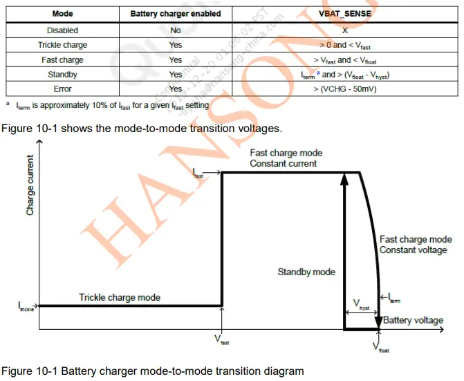
Battery Charger
The battery charger hardware is controlled by the on-chip application. The battery charger has 5 modes:
- Disabled
- Trickle charge
- Fast charge
- Standby: fully charged or float charge
- Error: charging input voltage, VCHG, is too low
Transitions between the trickle charge, fast charge and standby modes are triggered by changes in battery voltage and charger current.
Table 10-1 Battery charger operating modes determined by battery voltage and charger current
Power supply
The system have two power supply mode: Mode1: Single 3.3V only supply.
For improving the noise, recommend adding one 220Uf capacitor on the power supply pin
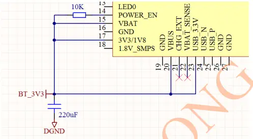
If the HSBT3007 is powered with an external 3.3 V supply connected to the VBAT line, Power_EN must be driven high after the IC has powered up otherwise the device may not initialise properly.
Mode2. Single 5V only supply.
A USB dongle is only powered when it is plugged into a USB port and does not need a switch to control the power.
POWER_EN should be left unconnected as the USB supply connected to the VCHG input will enable the IC correctly.
General Specifications
Absolute Maximum Ratings:
| Ratings | Min. | Max. | Unit |
| Storage Temperature | -40 | +105 | ℃ |
| Supply Voltage (VBUS) | -0.4 | 6.50 | V |
| Supply Voltage (POWER_EN) | -0.4 | 4.40 | V |
| Supply Voltage (LED[2:0]) | -0.4 | 4.40 | V |
| Supply Voltage (PIO_POWER) | -0.4 | 3.60 | V |
Recommended Operating Condition:
| Ratings | Min | Typ | Max | Unit |
| Operating Temperature range | -40 | 20 | +85 | ℃ |
| Supply Voltage (VBAT) | 2.50 | 3.70 | 4.40 | V |
| Supply Voltage (VBUS) | 4.75/3.10 | 5.00 | 6.50 | V |
| Supply Voltage (POWER_EN) | 0 | 3.70 | 4.40 | V |
| Supply Voltage (LED[2:0]) | – | 3.70 | 4.40 | V |
| Supply Voltage (PIO_POWER)* | 1.70 | 1.80 | 3.60 | V |
Regulator Enable
| POWER_EN,Switching Threshold | Min | Typ | Max | Unit |
| Rising threshold | – | – | 1.0 | V |
Battery Charger
| Battery Charger | Min | Type | Max | Unit |
| Input voltage, VCHG, 4.20 V float setting | 4.75 / 3.10a | 5.00 | 6.50 | V |
| Input voltage, VCHG, 4.35 V float setting | 4.90 / 3.10b | 5.00 | 6.50 | V |
a Reduced specification if VCHG – VBAT < 0.55 V. Full specification > 4.75 V. b Reduced specification if VCHG – VBAT < 0.55 V. Full specification > 4.90 V.
| Trickle | Charge | Mode | Min | Unit |
| Charge current Itrickle , as percentage of fast charge current | 8 | 10 | 12 | V |
| Vfast rising threshold | – | 2.9 | – | V |
| Vfast rising threshold trim step size | – | 0.1 | – | V |
| Vfast falling threshold | – | 2.8 | – | V |
| Fast Charge Mode | MIn | Typ | Max | Unit | |
| Charge current during constant current mode, Ifast | Maximum charge setting (VCHG – VBAT > 0.55 V) | 194 | 200 | 206 | mA |
| Minimum charge setting (VCHG – VBAT > 0.55 V) | – | 10 | – | mA | |
| Reduced headroom charge current, as a percentage of Ifast | (VCHG – VBAT < 0.55 V) | 50 | – | 100 | % |
| Charge current step size | – | 10 | – | mA | |
| V float threshold, 4.20 V | 4.16 | 4.20 | 4.24 | V | |
| V float threshold, 4.35 V | 4.31 | 4.35 | 4.39 | V | |
| Charge termination current Iterm, as percentage of Ifast | 7 | 10 | 20 | % | |
| Standby Mode | MIn | Typ | Max | Unit |
| Voltage hysteresis on VBAT, Vhyst | 100 | – | 150 | mV |
| Error Charge Mode | MIn | Typ | Max | Unit |
| Headroom(a) error rising threshold | – | 50 | – | mV |
(a) Headroom=VCHG-VBAT
| External Charge Mode | MIn | Typ | Max | Unit |
| Fast charge current, Ifast | 200 | – | 500 | mA |
| Control current into CHG_EXT | 0 | – | 20 | mA |
| Voltage on CHG_EXT | 0 | – | 6.50 | V |
| External pass device hfe | – | 50 | – | – |
| Sense voltage, between VBAT_SENSE and VBAT at maximum current | 195 | 200 | 205 | mV |
In the external mode, the battery charger meets all the previous charger electrical characteristics and the additional or superseded electrical characteristics are listed in this table.
LED Driver Pads
| LED Driver Pads | Min | Typ | Max | Unit | |
| Current, IPAD | High impedance state | – | – | 5 | uA |
| Current sink state | – | – | 10 | mA | |
| LED pad voltage, VPAD | IPAD = 10mA | – | – | 0.55 | V |
| VOL output logic level low(a) | – | 0 | – | V | |
| VOH output logic level high(a) | – | 0.8 | – | V | |
| VIL input logic level low | – | 0 | – | V | |
| VIH input logic level high | – | 0.8 | – | V | |
Layout Notes
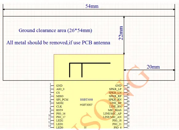
- If there is battery, metal, LCD, loudspeaker, etc. beside the module antenna, it is required to be at least 15mm away from the antenna
- It is recommended to use star routing for the power supply line during layout, and ensure that the power supply linearity of Bluetooth module is good, and the ground of BT is also availableIt must be separated from the ground of operational amplifier, power amplifier, MCU, etc., and there shall be no other interference ground under BT
- Do not walk around the antenna control line, power line, audio line, MIC and other interference lines
- If there is a row base near the module antenna and the shell has metal iron mesh which has an impact on the signal, it is recommended to select a professional high-rise heater beneficial antenna
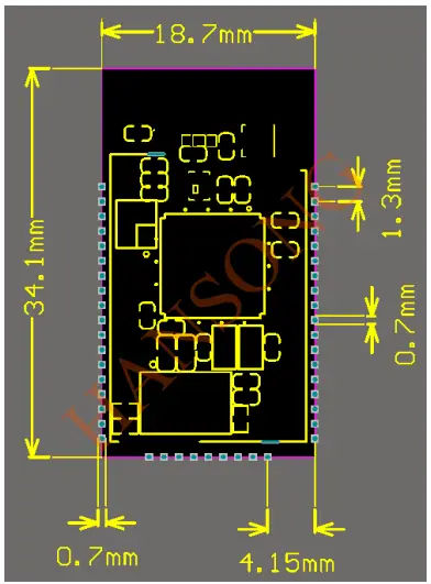
Dimension
Reflow temperature
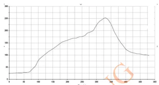
Key features of the profile:
- Initial Ramp=1-2.5’C/sec to 175C
- Equilibrium time=60 to 80 seconds
- Ramp to Maximum temperature (250C=3C/sec Max
- Time above liquidus temperature(217C): 45 -90 seconds
- Device absolute maximum reflow temperature: 250C equilibrium
FCC Statement
This equipment has been tested and found to comply with the limits for a Class B digital device, pursuant to Part 15 of the FCC Rules.
These limits are designed to provide reasonable protection against harmful interference in a residential installation. This equipment generate, uses and can radiate radio frequency energy and, if not installed and used in accordance with the instructions, may cause harmful interference to radio communications. However, there is no guarantee that interference will not occur in a particular installation. If this equipment does cause harmful interference to radio or television reception, which can be determined by turning the equipment off and on, the user is encouraged to try to correct the interference by one of the following measures:
- Reorient or relocate the receiving antenna.
- Increase the separation between the equipment and receiver.
- Connect the equipment into an outlet on a circuit different from that to which the receiver is connected.
- Consult the dealer or an experienced radio/TV technician for help.
This device complies with Part 15 of the FCC Rules. Operation is subject to the following two conditions:
- This device may not cause harmful interference, and
- this device must accept any interference received, including interference that may cause undesired operation.
Caution: Any changes or modifications not expressly approved by the party responsible for compliance could void the user’s authority to operate this equipment.
RF exposure warning
This equipment complies with FCC radiation exposure limits set forth for an uncontrolled environment. This equipment must be installed and operated in accordance with provided instructions and the antenna(s) used for this transmitter must be installed to provide a separation distance of at least 20 cm from all persons and must not be collocated or operating in conjunction with any other antenna or transmitter.
OEM Integration Instructions
This device is intended only for OEM integrators under the following conditions:
The module can be used to installation in other host. The antenna(s) used for this transmitter must be installed to the provided separation distance of at least 20cm from all persons and must not be co-located or operating in conjunction with any other antenna or transmitter. The module shall be only used with the integral antenna(s) that has been originally tested and certified with this module. As long as 3 conditions above are met, further transmitter test will not be required. However, the OEM integrator is still responsible for testing their end-product for any additional compliance requirement with this module installed (for example, digital device emission, PC peripheral requirements, etc.)
IC Statement
This device complies with Industry Canada license-exempt RSS standard(s). Operation is subject to the following two conditions:
(1) this device may not cause interference, and
(2) this device must accept any interference, including interference that may cause undesired operation of the device.
Caution: Modifications to this product will void the user’s authority to operate this equipment.
RF exposure warning
This equipment complies with IC radiation exposure limits set forth for an uncontrolled environment. This equipment must be installed and operated in accordance with provided instructions and the antenna(s) used for this transmitter must be installed to provide a separation distance of at least 20 cm from all persons and must not be collocated or operating in conjunction with any other antenna or transmitter. This radio transmitter IC: 7756A-QCC3007 has been approved by Innovation, Science and Economic Development Canada to operate with the antenna types listed below, with the maximum permissible gain indicated. Antenna types not included in this list that have a gain greater than the maximum gain indicated for any type listed are strictly prohibited for use with this device.
antenna type and gain:
- Onboard PCB Antenna 1.14dBi,
- External PCB Antenna 2.00dBi,
- External Dipole Antenna 2.93dBi.
- antenna impedance: 50Ω
OEM Integration Instructions
This device is intended only for OEM integrators under the following conditions: The module can be used to installation in other host. The antenna(s) used for this transmitter must be installed to the provided separation distance of at least 20cm from all persons and must not be co-located or operating in conjunction with any other antenna or transmitter. The module shall be only used with the integral antenna(s) that has been originally tested and certified with this module. As long as 3 conditions above are met, further transmitter test will not be required. However, the OEM integrator is still responsible for testing their end-product for any additional compliance requirement with this module installed (for example, digital device emission, PC peripheral requirements, etc.)


