![]()
![]()
Reference Guide
Forward Collision Warning (FCW) Application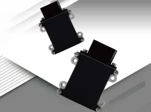
INTRODUCTION
The 79 GHz Radar Sensor uses Frequency-Modulated Continuous-Wave (FMCW) radar technology to detect whether there are moving objects in the areas around the vehicle that cannot be directly observed by the driver. These areas are called blind spot areas around the vehicle. 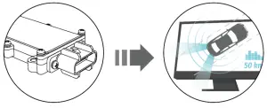
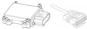
PACKAGE CONTENTS
The following items should be included in the packaging:
- 79 GHz Radar Sensor
- UART cable with a 10-pin connector
- Mounting accessories
NOTE: If any of the items, mentioned above, is not included in the packaging or are damaged in any way, contact your reseller immediately.
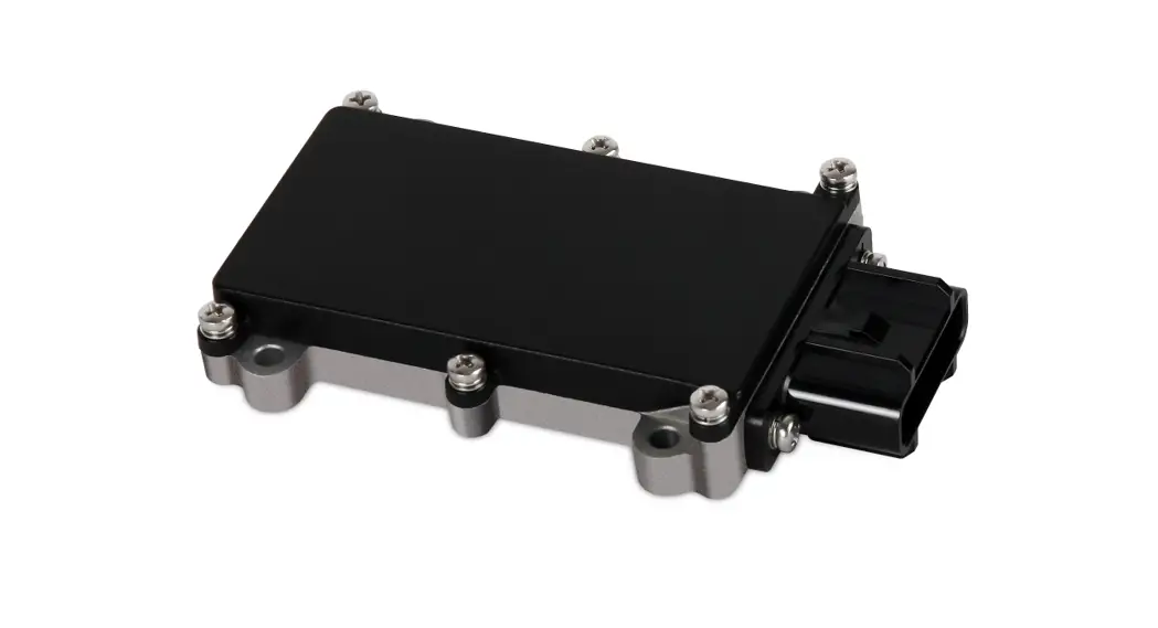
HARDWARE
The front and back panels of the radar sensor consist of different materials. The following diagrams will illustrate the front and back view of the radar sensor: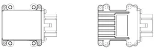
Front Panel – The front panel is made from plastic to prevent radar signal loss and promote the projection of a directional radar signal.
Back Panel – The back panel is made from metal. Metal will prevent the radar signal from reaching the inside of the vehicle.|
INSTALLATION
In this section, we’ll discuss the successful installation of the radar sensor onto the rear corners of most vehicles.
- Unbox the radar sensor and remove the rear bumper from the vehicle.
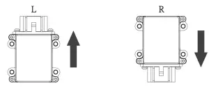
- The radar sensor can be installed onto the rear-left and/or rear-right corner of the vehicle with the metal side facing the vehicle.
- When the radar sensor is installed onto the rear-left corner of the vehicle, the cable should be facing upwards.
- When the radar sensor is installed onto the rear-right corner of the vehicle, the cable should be facing downwards.
3. The radar sensors should be installed facing backward with:
- The left-rear sensor rotated clockwise by 25 degrees.
- The right-rear sensor rotated anti-clockwise by 25 degrees.
4. The radar sensor should be mounted onto the vehicle at a 90degree angle, perpendicular to the ground.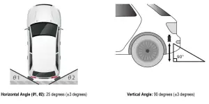
Horizontal Angle (θ1, θ2): 25 degrees (±3 degrees) Vertical Angle: 90 degrees (±3 degrees)
The radar sensor should be mounted onto the vehicle between 60 cm and 80 cm from the ground.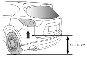
- When installation and testing are complete, the bumper can be re-installed onto the vehicle. The space between the bumper and the radar sensor must be at least 1 cm wide. No electronic/electric products or equipment that contain metal should be between the radar sensor and the area of detection.
TESTING
In this section, we’ll discuss how to test/calibrate the radar sensor to ensure that the radar sensor is working properly. An object, containing metal, with a height of at least 120 cm and a diameter of at least 21 cm, can be used to test the range and reliability of the radar detection area. A good example of an object that can be used for testing is a plastic pipe/tube wrapped with aluminum foil.
NOTE: Radar detection is based on movement. The person that moves the testing object should stand in line with the object for more accurate test results.
Two test areas (each 400 cm by 400 cm) should be cleared of any obstacles at the rear corners of the vehicle, as shown in the following diagram: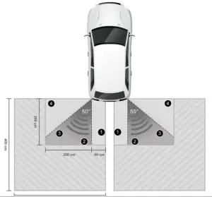
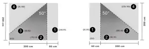
The detection area of the radar sensor, operating in ‘Mode 1’, is 200 cm by 200 cm. With an operating angle of 50 degrees, the true shape of the detection area will be more triangular than rectangular, as indicated in the diagram above. For practical purposes, let’s refer to the triangular detection area as the real detection area.
Starting from the bottom left corner (0 cm, 0cm); measure and mark out the following positions that will be used in the test:
| Left-rear corner: Position 1 240 cm from the left, 55 cm from the bottom Position 2: 170 cm from the left, 15 cm from the bottom Position 3: 60 cm from the left, 50 cm from the bottom Position 4: 25 cm from the left, 180 cm from the bottom | Right-rear corner: Position 1: 20 cm from the left, 55 cm from the bottom Position 2: 90 cm from the left, 15 cm from the bottom Position 3: 200 cm from the left, 50 cm from the bottom Position 4: 235 cm from the left, 180 cm from the bottom |
When the test metal object is placed on positions 1 and 4, the radar sensor should not detect an obstruction.
When the test metal object is placed on positions 2 and 3 the radar sensor should detect an obstruction.
In the diagrams below, the closest corner of the real detection area (triangular shape) will start right below the radar sensor and in line with the inside edge of the closest wheel on the vehicle.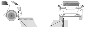
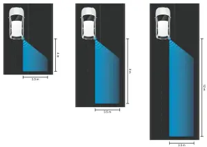
The operation “Mode” can be specified through the UART interface using terminal software like “PuTTY”. The default mode is Mode 1. The three modes that can be specified are:
| Mode “1” (BSD) – This mode is used to detect vehicles, overtaking/passing our vehicle from behind, from 4 meters back, between the speeds of 30~50 km/h. The maximum width right/left is one lane wide. | Mode “2” (LCA1) – This mode is used to detect vehicles, overtaking/passing our vehicle from behind, from 8 meters back, between the speeds of 50~80 km/h. The maximum width right/left is one lane wide. | Mode “3” (LCA2) – This mode is used to detect vehicles, overtaking/passing our vehicle from behind, from 12 meters back, between the speeds of 80 km/h and above. The maximum width right/left is one lane wide. |
TECHNICAL SPECIFICATIONS
SPECIFICATIONS
PHYSICAL & HARDWARE | |||
| Dimensions (L x W x H) | 78.3 mm x 61.8 mm x 19.8 mm | Weight | ?? kg |
| Housing Material (Rear) | Metal | Housing Material (Front) | Plastic |
| Material (Housing) | ??? PC (UL94v2) | Material Body | ??? Plastic/Metal |
| Chipset | TI AWR1642 | On-Chip Memory | 1.5 MB |
POWER | |||
| Supply Voltage | 12 VDC | Max. Power Consumption | 8 Watts |
RADAR SIGNAL | |||
| Frequency Range | 78 GHz to 81 GHz | Signal Range | Between 0.5 and 180 meters |
| FOV (Horizontal) | 60 degrees | FOV (Vertical) | 30 degrees |
| TX Power | 12.5 dBm | RX Noise Figure | 14 dB (76 to 79 GHz) |
| Channels | Receive 4, Transmit 2 | Phase Noise at 1 MHz | – 95 dBc/Hz (76 to 79 GHz) |
ENVIRONMENT | |||
| Operating Temperature | -40°C to 85°C | Storage Temperature | -??°C to ??°C |
| Operating Humidity | 10% to 90% (Non-condensing) | Storage Humidity | 0% to 95% (Non-condensing) |
CONNECTOR & CABLE | |||
| Cable Length | ??? centimeters/meters | Cable Type | ??? RG 316D |
| Cable Color | ??? | Connector Pinout | See here |
INTERFACE & SOFTWARE | |||
| Host Interface | CAN (Two instances, 1 x CAN- FD) | Built-in Firmware | ROM |
| ADC Channels | Up to 6 | SPI Channels | Up to 2 |
| UARTs | Up to 2 | Other | I2C, GPIOs |
STANDARDS
| STANDARD | DESCRIPTION |
| Regulatory Compliance | Comply with CE Markings per directives 2004/108/EC and 2006/95/EC |
| FCC/IC Report Class A | |
| UL/cUL Listed Mark | |
| Safety | UL/CSA-C22.2 NO. 60950-1-07 |
| EMC | EN 55022/EN 55024, Class A |
| FCC CFR47, Part 15B, Class A | |
| ICES-003, Class A | |
| IEC Standard 60529 | IP67 to IP69K Compliance |
| RoHS Directive | ??? |
| WEEE Directive | ??? |
APPENDIX
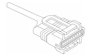
UART CABLE CONNECTOR PIN-OUT
The following table lists the connector pin-out descriptions of the Universal Asynchronous Receiver-Transmitter (UART) cable:
| PIN NUMBER | TYPE | COLOR | DESCRIPTION |
| 1 | GND | Black | Pin used for the ground connection. |
| 2 | 12 V | Red | Pin used for supplying 5 V power to the unit. |
| 3 | 12 V | Dark Red | Pin used for supplying 5 V power to the unit. |
| 4 | CANAL | Yellow | Controller Area Network Low (CANL) pin. |
| 5 | CANH | Purple | Controller Area Network High (CANH) pin. |
| 6 | GPIO 1 | Green | General-Purpose Input/Output 1 (GPIO 1) pin. |
| 7 | GPIO 0 | Orange | General-Purpose Input/Output 1 (GPIO 0) pin. |
| 8 | UART RX | Blue | Universal Asynchronous Receiver-Transmitter (UART) receive data pin. |
| 9 | UART TX | White | Universal Asynchronous Receiver-Transmitter (UART) transmit data pin. |
| 10 | GND | Grey | Pin used for the ground connection. |
GENERAL INPUT/OUTPUT PORT CHARACTERISTICS
| SYMBOL | PARAMETER | CONDITION | MIN | TYPE | MAX | UNIT |
| VIL | FT, FTP, TTa, and NRST I/O input low-level voltage | 1.7 V ≤ VDD ≤ 3.6 V | – | – | 0.35VDD – 0.04 |
V |
| 0.3VDD (2) | ||||||
| BOOT0 I/O input low-level voltage | 1.75 V ≤ VDD ≤ 3.6 V, – 40°C ≤ TA ≤105°C | – | – | 0.1VDD + 0.1 (1) | ||
| 1.7 V ≤ VDD ≤ 3.6 V, 0°C ≤ TA ≤ 105°C | – | – | ||||
| VIA | FT, FTP, TTa, and NRST I/O input high-level voltage (4) | 1.7 V ≤ VDD ≤ 3.6 V | 0.45 VDD + 0.3 (1) | – | – | V |
| 0.7 VDD(2) | ||||||
| BOOT0 I/O input high-level voltage | 1.75 V ≤ VDD ≤ 3.6 V, – 40°C ≤ TA ≤ 105°C | 0.17 VDD + 0.7 (1) | – | – | ||
| 1.7 V ≤ VDD ≤ 3.6 V, 0°C ≤ TA ≤ 105°C | ||||||
| PHYS | FT, FTP, TTa, and NRST I/O input hysteresis | 1.7 V ≤ VDD ≤ 3.6 V | – | 10% VDD | – | V |
| BOOT0 I/O input hysteresis | 1.75 V ≤ VDD ≤ 3.6 V, – 40°C ≤ TA ≤ 105°C | – | 100 m | – | ||
| 1.7 V ≤ VDD ≤ 3.6 V, 0°C ≤ TA ≤ 105°C | – | – | ||||
| Ilka | I/O input leakage current (3) | VSS ≤ VIN ≤ VDD | – | – | ±1 | µA |
| I/O FT input leakage current (4) | VIN = 5 V | – | – | 3 | ||
|
RPU | Weak pull-up equivalent resistor (5) All pins except for PA10/PB12 (OTG_FS_ID, OTG_HS_ID) | VIN = VSS | 30 | 40 | 50 | kΩ |
| Weak pull-up equivalent resistor (5) Pins PA10/PB12 (OTG_FS_ID, OTG_HS_ID) | 7 | 10 | 14 | |||
|
RPD | Weak pull-down equivalent resistor(6) All pins except for PA10/PB12 (OTG_FS_ID, OTG_HS_ID) | VIN = VDD | 30 | 40 | 50 | kΩ |
| Weak pull- down equivalent resistor (6) Pins PA10/PB12 (OTG_FS_ID, OTG_HS_ID) | 7 | 10 | 14 | |||
| CIO(7) | I/O pin capacitance | – | – | 5 | – | pF |
Footnotes:
- Guaranteed by design.
- Tested in production.
- Leakage could be higher than the maximum value if a negative current is injected on adjacent pins.
- To sustain a voltage higher than VDD + 0.3 V, the internal pull-up/pull-down resistors must be disabled. Leakage could be higher than the maximum value if negative current is injected on adjacent pins.
- Pull-up resistors are designed with a true resistance in series with a switchable PMOS. This PMOS contribution to the series resistance is minimum (~10% order).
- Pull-down resistors are designed with a true resistance in series with a switchable NMOS. This NMOS contribution to the series resistance is minimum (~10% order).
- Hysteresis voltage between Schmitt triggers switching levels. Guaranteed based on test during characterization.
OUTPUT VOLTAGE CHARACTERISTICS
| SYMBOL | PARAMETER | CONDITION | MIN | MAX | UNIT |
| VOL (1) | Output low-level voltage for an I/O pin | CMOS port (2) IIO = 8 mA 2.7 V ≤ VDD ≤ 3.6 V | – | 0.4 | V |
| VOH (3) | Output high-level voltage for an I/O pin | VDD – 0.4 | – | ||
| VOL (1) | Output low-level voltage for an I/O pin | TTL port (2) IIO = 8 mA 2.7 V ≤ VDD ≤ 3.6 V | – | 0.4 | V |
| VOH (3) | Output high-level voltage for an I/O pin | 2.4 | – | ||
| VOL (1) | Output low-level voltage for an I/O pin | IIO = 20 mA 2.7 V ≤ VDD ≤ 3.6 V | – | 1.3 (4) | V |
| VOH (3) | Output high-level voltage for an I/O pin | VDD – 0.4 (4) | – | ||
| VOL (1) | Output low-level voltage for an I/O pin | IIO = 6 mA 1.8 V ≤ VDD ≤ 3.6 V | – | 0.4 (4) | V |
| VOH (3) | Output high-level voltage for an I/O pin | VDD – 0.4 (4) | – | ||
| VOL (1) | Output low-level voltage for an I/O pin | IIO = 4 mA 1.7 V ≤ VDD ≤ 3.6V | – | 0.4 (5) | V |
| VOH (3) | Output high-level voltage for an I/O pin | VDD – 0.4 (5) | – |
Footnotes:
- The IIO current sunk by the device must always respect the absolute maximum rating and the sum of IIO (I/O ports and control pins) must not exceed IVSS.
- TTL and CMOS outputs are compatible with JEDEC standards JESD36 and JESD52.
- The IIO current sourced by the device must always respect the absolute maximum rating and the sum of IIO (I/O ports and control pins) must not exceed IVDD.
- Based on characterization data.
- Guaranteed by design.
FCC 15b devices (15.105)
This equipment has been tested and found to comply with the limits for a Class B digital device, pursuant to part 15 of the FCC rules. These limits are designed to provide reasonable protection against harmful interference in a residential installation. This equipment generates, uses, and can radiate radio frequency energy and, if not installed and used in accordance with the instructions, may cause harmful interference to radio communications. However, there is no guarantee that interference will not occur in a particular installation.
If this equipment does cause harmful interference to radio or television reception, which can be determined by turning the equipment off and on, the user is encouraged to try to correct the interference by one or more of the following measures:
‐Reorient or relocate the receiving antenna.
‐Increase the separation between the equipment and receiver.
‐Connect the equipment into an outlet on a circuit different from that to which the receiver is connected.
‐Consult the dealer or an experienced radio/TV technician for help.
FCC Part 15.21
Information for user
You are cautioned that changes or modifications not expressly approved by the party responsible for compliance could void your authority to operate the equipment.
FCC Part 15.19
This device complies with Part 15 of the FCC Rules. Operation is subject to the following two conditions: (1) this device may not cause harmful interference and (2) this device must accept any interference received, including interference that may cause undesired operation


