VTX-WBM-N12
User manual
Feb.2019
REVISION HISTORY
Version No. | Revised Date | Revised by | Description | Notes |
| 1.0 | 2019-03-15 | Sam | Preliminary User Manual released | Proposal |
| 1.1 | 2021 02 08 | Sam | Remove BT function | |
| 1.2 | 2021 02-22 | Stephen | Modify warning content |
INTRODUCTION
1.1 DESCRIPTION
VTX-WBM-N12 is a complete WiFi and MCU module which is designed for embedded wireless solutions and a cost-effective, low power capabilities high-performance MCU in IOT applications.
The module integrates ARM Cortex™ -M4 MCU with FPU, clock, WiFi, and front end. It is based on Cypress IEEE802.11 b/g/n single-stream. Thus, it can be used to enable wireless connectivity to the simplest existing sensor product with minimal engineering effort.
1.2 FEATURES
The module comprises the following functions
| MCU | STM32 ARM 32-bit Cortex™-M4 Frequency up to 100MHz |
| Memory capacity | 1 Mbyte of MCU internal Flash, |
| 256KB of SRAM, | |
| 2Mbyte of SPI Flash | |
| Diverse serial interface | SPI, Quad SPI (support Dual mode), USART, PCM |
| Sensor applications support | ADC, I2C, I2S, GPIO, Timers |
| Debug interface support | JTAG |
| On-chip functionality Single-chip | MAC/BB/RF |
| Frequency Band | 2.4 GHz |
| Network Standard | 802.11b, 802.11g, 802.11n (single stream) |
| Modulation Modes | WiFi: CCK and OFDM with BPSK, QPSK, 16QAM, 64QAM, 256QAM |
| Hardware Encyption | WEP, WPA/WPA2 |
| Supported Data Rates | IEEE 802.11b 1 – 11 Mbps |
| IEEE 802.11g 6 – 54 Mbps | |
| IEEE802.11n (2.4 GHz) 7.2 – 150 Mbps | |
| Advanced 1×1 802.11n features | Full/Half Guard Interval |
| Fram Aggregation | |
| Space Time Block coding (STBC) | |
| Low Density Parity Check (LDPC) Encoding | |
| BRCM WICED Fully compatible | |
| Operating Temperature | 40℃ to 85 ℃ |
| Antenna |
| Gain | Type | Connector |
| 5.05 dBi | Chip Antenna | Fixed |
| 5.09 dBi | Dipole Antenna | SMA |
BLOCK DIAGRAM
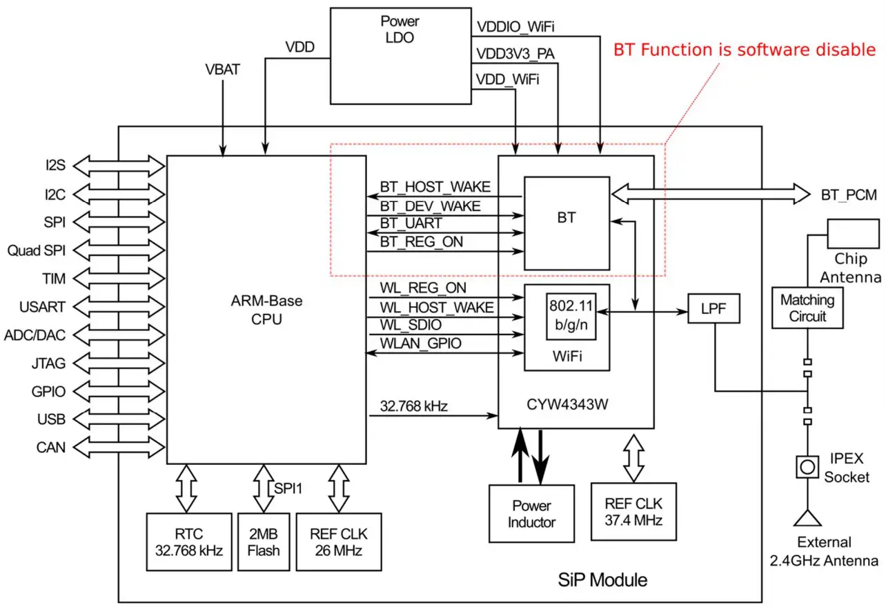
| ADC | Analog to Digital Converter |
| DAC | Digital to Analog Converter |
| I2C | Intelligent Interface Controller |
| SPI | Serial Peripheral Interface |
| Quad SPI | Quad Serial Peripheral Interface |
| USART | Universal synchronous/asynchronous receiver transmitters |
| TIM | Timers |
| I2S | Inter-integrated sound |
| CAN | Controller area network |
MODULE DESCRIPTION
3.1 MODULE APPEARANCE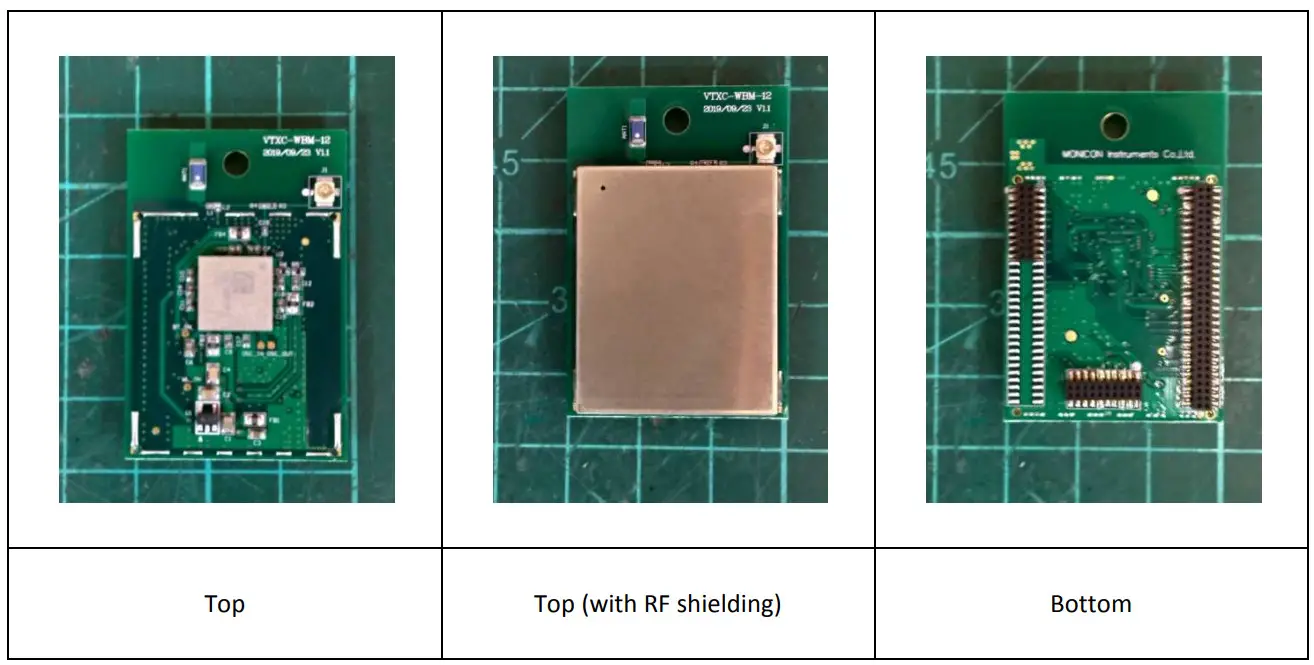
3.2 COMPONENT DESCRIPTION
| J1 | External antenna socket |
| ANT1 | Onboard chip antenna |
| R3 | Jump for external antenna using |
| R4 | Jump for chip antenna using |
3.3 ANTENNA LIST
| Antenna 1 | |
| Antenna Gain | : 5.05 dBi |
| Antenna Type | : Chip Antenna |
| Connector Type | : Fixed |
| Antenna 2 | |
| Antenna Gain | : 5.09 dBi |
| Antenna Type | : Dipole Antenna |
| Connector Type | : SMA |
3.4 FCC COMPLIANCE
The module has been tested for compliance with FCC Part 15.247
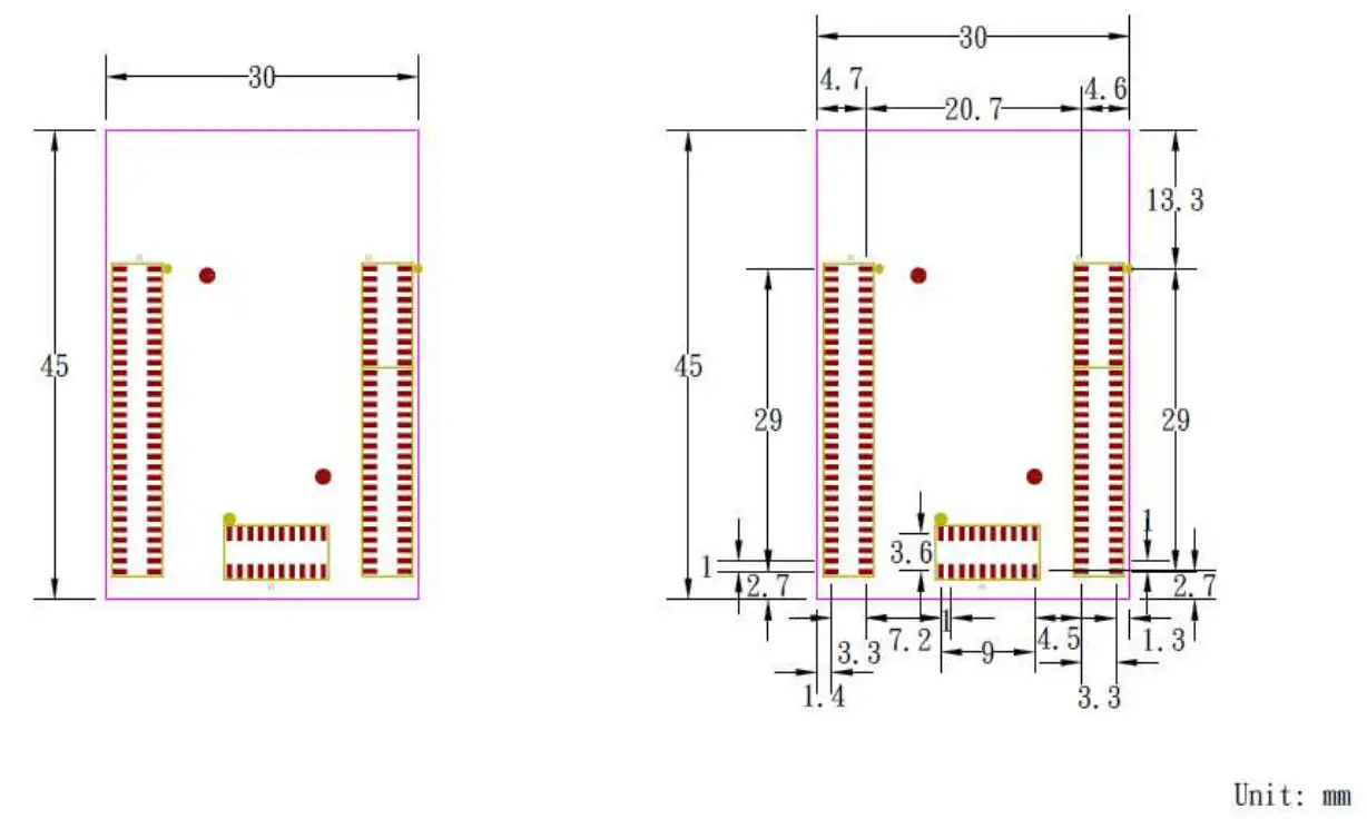
3.5 DIMENSION
ADDITION INFORMATION
4.1 I2C INTERFACE
Characteristics
| Symbol | Parameter | Standard modem(1) | Fast mode(2) | Unit | ||
| Min | Max | Min | Max | |||
| tw(SCLL) | SCL clock low time | 4.7 | – | 1.3 | – | μs |
| tw(SCLH) | SCL clock high time | 4.0 | – | 0.6 | – | |
| tsu(SDA) | SDA setup time | 250 | – | 100 | – | ns |
| th(SDA) | SDA data hold time | 0 | 3450(3) | 0 | 900(4) | |
| tr(SDA) tr(SDL) | SDA and SCL rise time | – | 1000 | – | 300 | |
| tf(SDA) tf(SDL) | SDA and SCL fall time | – | 300 | – | 300 | |
| th(STA) | Start condition hold time | 4.0 | – | 0.6 | – | μs |
| tsu(STA) | Repeated Start condition setup time | 5. | – | 0.6 | – | μs |
| tsu(STO) | Stop condition setup time | 4.0 | – | 0.6 | – | μs |
| tw(STO:STA) | Stop to Start condition time (bus free) | 5. | – | 1. | – | |
| tSP | The pulse width of the spikes that are suppressed by the analog filter for standard fast mode | 0 | 50(5) | 0 | 50(5) | μs |
| Cb | Capacitive load for each bus line | – | 400 | – | 400 | pF |
- Guaranteed by design, not tested in production.
- fPCLK1 must be at least 2MHz to achieve standard mode I2C frequencies. It must be at least 4MHz to achieve fast mode I2C frequencies, and a multiple of 10MHz to reach the 400kHz maximum I2C fast mode clock.
- The device must internally provide a hold time of at least 300ns for the SDA signal in order to bridge the undefined region of the falling edge of the SCL
- The maximum data hold time has only to be met if the interface does not stretch the low period of the SCL signal.
WARNING
Federal Communication Commission Interference Statement
15.19
This device complies with Part 15 of the FCC Rules. Operation is subject to the following two conditions: (1) this device may not cause harmful interference, and (2) this device must accept any interference received, including interference that may cause undesired operation.
15.105
This equipment has been tested and found to comply with the limits for a Class B digital device, pursuant to part 15 of the FCC Rules. These limits are designed to provide reasonable protection against harmful interference in a residential installation. This equipment generates, uses, and can radiate radio frequency energy and, if not installed and used in accordance with the instructions, may cause harmful interference to radio communications.
However, there is no guarantee that interference will not occur in a particular installation. If this equipment does cause harmful interference to radio or television reception, which can be determined by turning the equipment off and on, the user is encouraged to try to correct the interference by one or more of the following measures:
- Reorient or relocate the receiving antenna.
- Increase the separation between the equipment and receiver.
- Connect the equipment into an outlet on a circuit different from that to which the receiver is connected.
- Consult the dealer or an experienced radio/TV technician for help.
FCC RF Radiation Exposure Statement:
This module is intended for OEM integrators. The OEM integrator is still responsible for the FCC compliance requirement of the end product, which integrates this module. 20cm minimum distance has to be able to be maintained between the antenna and the users for the host this module is integrated into. Under such a configuration, the FCC radiation exposure limits set forth for a population/uncontrolled environment can be satisfied.
Any changes or modifications not expressly approved by the manufacturer could void the user’s authority to operate this equipment. The module has been tested for compliance with FCC Part 15.247.
USERS MANUAL OF THE END PRODUCT:
In the user’s manual of the end product, the end-user has to be informed to keep at least 20cm separation with the antenna while this end product is installed and operated. The end-user has to be informed that the FCC radio-frequency exposure guidelines for an uncontrolled environment can be satisfied. The end-user has to also be informed that any changes or modifications not expressly approved by the manufacturer could void the user’s authority to operate this equipment.
If the size of the end product is smaller than 8x10cm, then an additional FCC part 15.19 statement is required to be available in the users manual:
This device complies with Part 15 of FCC rules. Operation is subject to the following two conditions: (1) this device may not cause harmful interference and (2) this device must accept any interference received, including interference that may cause undesired operation.
LABEL OF THE END PRODUCT:
The final end product must be labeled in a visible area with the following ” Contains TX FCC ID:
2AXR2VTC-WM-N12V01 “. If the size of the end product is larger than 8x10cm, then the following FCC part 15.19 statement has to also be available on the label: This device complies with Part 15 of FCC rules. Operation is subject to the following two conditions: (1) this device may not cause harmful interference and (2) this device must accept any interference received, including interference that may cause undesired operation.
Industry Canada statement:
This device complies with Industry Canada’s license-exempt RSSs. Operation is subject to the following two conditions:
(1) This device may not cause interference; and
(2) This device must accept any interference, including interference that may cause undesired operation of the device.
Radiation Exposure Statement:
OEM integrator is still responsible for testing their end-product for any additional compliance requirements required with this module installed (for example, digital device emissions, PC peripheral requirements, etc.).
IMPORTANT NOTE:
In the event that these conditions cannot be met (for example certain laptop configurations or co-location with another transmitter), then the IC authorization is no longer considered valid and the IC No. cannot be used on the final product. In these circumstances, the OEM integrator will be responsible for re-evaluating the end product (including the transmitter) and obtaining a separate IC authorization.
USERS MANUAL OF THE END PRODUCT:
The OEM integrator has to be aware not to provide information to the end-user regarding how to install or remove this RF module in the user’s manual of the end product which integrates this module.
The end-user manual shall include all required regulatory information/warning as shown in this manual.
LABEL OF THE END PRODUCT:
This transmitter module is authorized only for use in devices where the antenna may be installed such that 20 cm may be maintained between the antenna and users. The final end product must be labeled in a visible area with the following: “Contains transmitter module IC: 26568- VTCWMN12V01 “


