![]()
Quick Start Guide
for tM-DA1P1R1
April. 2014, Version 1.20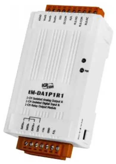
Congratulations
Congratulations on purchasing the tM-DA1P1R1 the most popular automation solution for remote monitoring and control applications. This Quick Start Guide will provide
the information needed to get started with the tM-DA1P1R1. Please also consult the User Manual for detailed information on the setup and use of the tM-DA1P1R1.
What’s in the shipping box?
In addition to this guide, the shipping box includes the following items: 
Technical Support
- ICP DAS Website
http://www.icpdas.com/
- Understanding the Hardware Specifications and Wiring Diagrams
Before installing the hardware, you should h ave a basic understanding of hardware specifications and the wiring diagrams.
System Specifications :
| Communication | |
| Interface | RS-485 |
| Format | (N, 8, 1), (N, 8, 2), (O, 8, 1), (E, 8, 1) |
| Baud Rate | 1200 ~ 115200 bps |
| Protocol | DCON, Modbus/RTU, Modbus/ASCII |
| Watchdog | Communication (Programmable) |
| LED Indicators | |
| Power | 1 LED as Power Indicator |
| Isolation | |
| Intra-module Isolation, Filed-to-Logic | 2500 VDC |
| EMS Protection | |
| ESD (IEC 61000-4-2) | ±4 kV contact for Each Terminal |
| ±8 kV Air for Random Point | |
| EFT (IEC 61000-4-4) | ±4 kV for Power Line |
| Power | |
| Reverse Polarity Protection | Yes |
| Input Range | 10 ~ 30 VDC |
| Consumption | 1.8 W max. |
| Mechanical | |
| Dimensions ( W x L x H ) | 52 mm x 98 mm x 27 mm |
| Installation | DIN-Rail Mounting |
| Environment | |
| Operating Temperature | -25 ~ +75 °C |
| Storage Temperature | -30 ~ +80 °C |
| Humidity | 10 ~ 95% RH, Non-condensing |
I/O Specifications :
| Analog Output | ||
| Channel | 1 | |
| Type | 0~10V, 0~20mA, 4~20mA | |
| Resolution | 12-bit | |
| Accuracy | ±0.1% of FSR | |
| DA Output Response Time | 10 ms | |
| Voltage Output Capability | 20 mA | |
| Current Load Resistance | 500 Ω | |
| Digital Input/Counter | ||
| Channel | 1 | |
| Type | Dry | |
| On Voltage Level | Close to GND | |
| Off Voltage Level | Open | |
| Counters | Max. Counts | 65536 (16-bit) |
| Max. Input Frequency | 100 Hz | |
| Min. Pulse Width | 5 ms | |
| Input Impedance | 10 KΩ | |
| Relay Output | ||
| Channel | 1 | |
| Type | Power Relay, Form C | |
| Operating Load Voltage Range | 250 VACor 30 VDC | |
| Max. Load Current | NO : 10 A @250 VAC NC : 6 A @250 VAC | |
| Operate Time | 15 ms max. | |
| Release Time | 5 ms max. | |
| Mechanical Endurance | 1 X 10⁷ OPS | |
| Electrical Endurance | 5 X 10⁴ OPS | |
| Power On and Safe Value | Yes, Programmable | |
Wire Connection:
Voltage Output | |
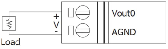 | |
Current Output | |
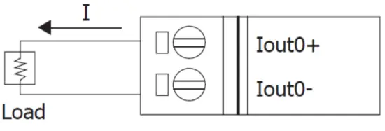 | |
Digital Input/Counter | |
| ON State Readback as 1 | OFF State Readback as 0 |
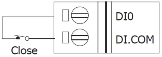 | 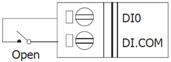 |
| Relay Output | |
| ON State | OFF State |
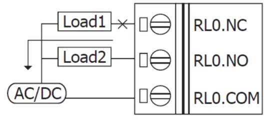 | 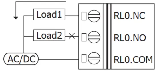 |
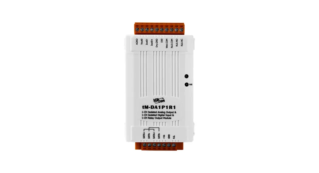
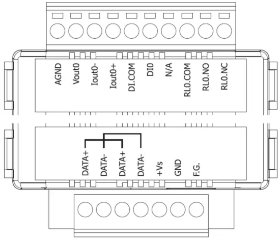
Pin Assignment :

2 Booting the tM-Series in Init Mode
Make sure the switch is placed in the “Init” position.
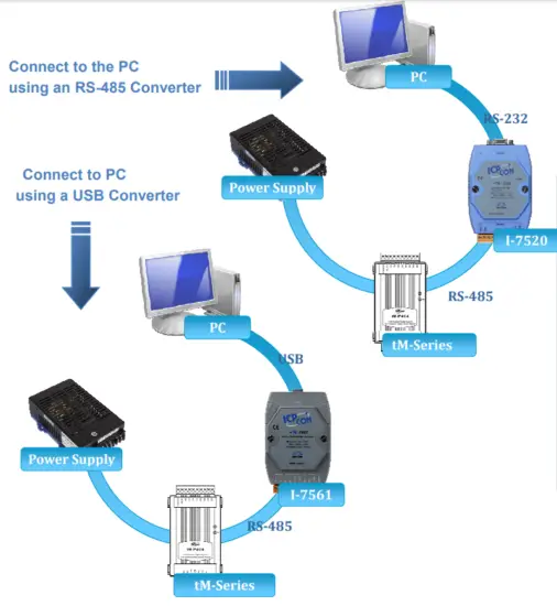
Connecting to the PC and the Power Supply
The tM-Series series is equipped with an RS-485 port for connection to a 232/USB converter to PC
Installing the DCON Utility
The DCON Utility is an easy-to-use tool designed to enable simple configuration of I/O modules that use the DCON protocol.
Step 1: Locate the DCON Utility

The DCON Utility can be obtained from the companion CD or from the ICPDAS FTP site:
CD:\Napdos\8000\NAPDOS\Driver\DCON_Utility\setup\
http://ftp.icpdas.com/pub/cd/8000cd/napdos/driver/dcon_utility/
Step 2: Follow the prompts to complete the installation

After the installation has been completed, there will be a new shortcut to the DCON Utility on the desktop.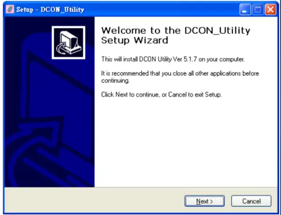
5 Using the DCON Utility to Initialize the TM-Series Module
The M-Series is an I/O module based on the DCON protocol, meaning that you can use the DCON Utility to easily initialize it.
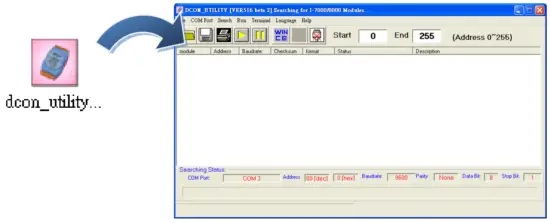
Step 1: Run the DCON Utility
Double-click the DCON Utilityshortcut on your desktop.
Step 2: Use the COM1 port to communicate with the tM-Series
Click the “COM Port” option from the menu and a dialog box will be displayed that will allow you to set the communication parameters as described in the table below.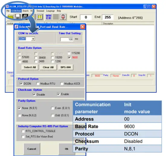
Step 3: Search for the TM-Series module
Click the “Start Search” button from the toolbox to search for the tM-Series module. After the TM-Series module is displayed in the list, click the “Stop Search” button.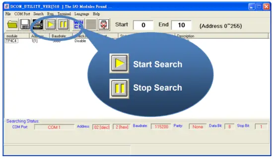
Step 4: Connect to the tM-Series
After clicking on the name of the module in the list, a dialog box will be displayed. 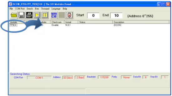
Step 5: Initialize the TM-Series module
Set the “Address” field in the dialog box to 1 and then click the “Setting” button to save the settings.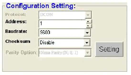

6 Rebooting the TM-SeriesModule in Normal Mode
Make sure the INIT switch is placed in the “Normal” position.
Starting the Module Operation
After rebooting the TM-Series module, search for the module to make sure the settings have been changed. You can double-click on the name of the module in the list to open the configuration dialog box. 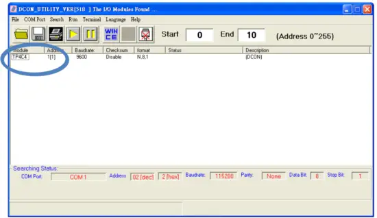
DCON Command Sets
| Command | Description |
| $AAF | read firmware version |
| $AAI | read INIT status response: !AA0 -> INIT short to GND !AA1 -> else |
| $AAM | read module name |
| $AAP | Read Modbus RTU/DCON protocol response: !AA0 -> DCON !AA1 -> Modbus RTU |
| $AAPN | Set Modbus RTU/DCON protocol N-> 0: DCON, 1: Modbus RTU |
| $AA00 | channel 0 AO zero calibration |
| $AA10 | channel 0 AO span calibration |
| $AA2 | read configuration |
| $AA30VV | trim the channel 0 analog output, VV in hex, 01-7F to increase, FF-80 to decrease |
| $AA40 | set current analog output as power-on value of channel 0 |
| $AA5 | read reset status !AA1 first after power on, !AA0 others |
| $AA60 | read back the last analog output value set by the analog output command of channel 0 |
| $AA70 | read the power on value of the analog output channel 0 |
| $AA80 | read back the current analog output value of channel 0 |
| $AA90 | read the type code and slew rate of analog output channel 0 |
| $AA90TS | set the type code (T) and slew rate (S) of analog output channel 0 |
| #AA0(data) | set analog output value of channel 0 |
| %AANNTTCCFF | set configuration, NN: new address, TT = 00, CC: new baud rate FF: data format |
| @AACEC0 | clear DI counter 0 |
| Command | Description |
| @AADI | read DIO response !AA00O0I |
| @AADO0V | set DO, V-> 0: off, 1: on |
| @AAREC0 | read event counter of channel 0 |
| ~** | clear host watchdog timeout counter |
| ~AA0 | read host watchdog status |
| ~AA1 | clear host watchdog timeout status |
| ~AA2 | read host watchdog enable/disable status and timeout value |
| ~AA3ETT | enable/disable host watchdog and set timeout value E-> 0: disable host watchdog, 1: enable host watchdog TT: host watchdog timeout in 0.1s in hex format |
| ~AA4 | read DO power on and safe value |
| ~AA40 | read analog output channel 0 safe value |
| ~AA50P0S | set DO power on and safe value P-> 0: power on value off, 1: power on value on S-> 0: safe value off, 1: safe value on |
| ~AAO(name) | set module name |
| ~AARD | read response delay time in ms in hex format |
| ~AARDVV | set response delay time in ms, VV in hex format, 00 – 1E |
Baud Rate Setting (CC) Bits 5:0
Baud rate, 0x03 ~ 0x0A
| Code | 0x03 | 0x04 | 0x05 | 0x06 |
| Baud | 1200 | 2400 | 4800 | 9600 |
| Code | 0x07 | 0x08 | 0x09 | 0x0A |
| Baud | 19200 | 38400 | 57600 | 115200 |
Bits 7:6
00: no parity, 1 stop bit
01: no parity, 2 stop bits
10: even parity, 1 stop bit
11: odd parity, 1 stop bit
Data Format Setting (FF)
Bits 1:0
00: engineering format
01: percent format
10: hex format
Bits 6
0: checksum disabled
0: checksum enabled
Type Code Setting (T)
| Type Code | Output Range | Data Format | Max | Min |
| 0 | 0 ~ 20 mA | Engineering | +20.000 | +00.000 |
| Percent | +100.00 | +000.00 | ||
| Hexadecimal | FFFFh | 0000h | ||
| 1 | 4 ~ 20 mA | Engineering | +20.000 | +04.000 |
| Percent | +100.00 | +000.00 | ||
| Hexadecimal | FFFFh | 0000h | ||
| 2 | 0 ~ 10 V | Engineering | +10.000 | +00.000 |
| Percent | +100.00 | +000.00 | ||
| Hexadecimal | FFFFh | 0000h | ||
| 4 | 0 ~ 5 V | Engineering | +05.000 | +00.000 |
| Percent | +100.00 | +000.00 | ||
| Hexadecimal | FFFFh | 0000h |
Slew Rate Setting (S)
| S | V/s | mA/s | S | V/s | mA/s |
| 0 | Immediate | Immediate | 8 | 8.0 | 16.0 |
| 1 | 0.0625 | 0.125 | 9 | 16.0 | 32.0 |
| 2 | 0.125 | 0.25 | A | 32.0 | 64.0 |
| 3 | 0.25 | 0.5 | B | 64.0 | 128.0 |
| 4 | 0.5 | 1.0 | C | 128.0 | 256.0 |
| 5 | 1.0 | 2.0 | D | 256.0 | 512.0 |
| 6 | 2.0 | 4.0 | E | 512.0 | 1024.0 |
| 7 | 4.0 | 8.0 |
Modbus Address Mapping
| Address | Description | Attribute |
| 10097 | Low latched values of DI | R |
| 10105 | Low latched values of DO | R |
| 00001 | Digital output value of channel 0 | R/W |
| 00033 | Digital input value of channel 0 | R |
| 00065 | High latched values of DI | R |
| 00073 | High latched values of DO | R |
| 00097 | Low latched values of DI | R |
| 00105 | Low latched values of DO | R |
| 00129 | Safe value of digital output channel 0 | R/W |
| 00161 | Power on value of digital output channel 0 | R/W |
| 00193 | Counter update trigger edge of channel 0 | R/W |
| 00513 | Write 1 to clear counter value of channel 0 | W |
| 00257 | Protocol, 0: DCON, 1: Modbus RTU | R/W |
| 00258 | 0: Modbus RTU, 1: Modbus ASCII | R/W |
| 00260 | Modbus host watchdog mode 0: same as I-7000 1: can use AO and DO commands to clear the host watchdog timeout status | R/W |
| 00261 | 1: enable, 0: disable host watchdog | R/W |
| 00264 | Write 1 to clear latched DIO | W |
| 00265 | DI active state, 0: normal, 1: inverse | R/W |
| 00266 | DO active state, 0: normal, 1:inverse | R/W |
| 00269 | Modbus data format, 0: hex, 1: engineering | R/W |
| 00270 | Host watchdog timeout status, write 1 to clear host watchdog timeout status | R/W |
| 00273 | Reset status, 1: first read after powered on, 0: not the first read after powering on | R |
| 30065 | Analog output read back | R |
| 30129 | The counter value of digital input | R |
| 40033 | Analog output value | R/W |
| 40097 | Safe analog output value | R/W |
| 40193 | Power on the analog output value | R/W |
| Address | Description | Attribute | |||||
| 40289 | Analog output slew rate | R/W | |||||
| 40417 | Analog output type code | R/W | |||||
| 40481 | Firmware version (low word) | R | |||||
| 40482 | Firmware version (high word) | R | |||||
| 40483 | Module name (low word) | R | |||||
| 40484 | Module name (high word) | R | |||||
| 40485 | Module address, valid range: 1 ~ 247 | R/W | |||||
| 40486 | Bits 5:0 Baud rate, 0x03 ~ 0x0A | R/W | |||||
| Code | 0x03 | 0x04 | 0x05 | 0x06 | |||
| Baud | 1200 | 2400 | 4800 | 9600 | |||
| Code | 0x07 | 0x08 | 0x09 | 0x0A | |||
| Baud | 19200 | 38400 | 57600 | 115200 | |||
| Bits 7:6 00: no parity, 1 stop bit 01: no parity, 2 stop bits 10: even parity, 1 stop bit 11: odd parity, 1 stop bit | |||||||
| 40488 | Modbus response delay time in ms, valid range: 0 ~ 30 | R/W | |||||
| 40489 | Host watchdog timeout value, 0 ~ 255, in 0.1s | R/W | |||||
| 40492 | Host watchdog timeout count, write 0 to clear | R/W | |||||
| 10033 | Digital input value of channel 0 | R | |||||
| 10065 | High latched values of DI | R | |||||
| 10073 | High latched values of DO | R | |||||
| Type Code | Output Range | Data Format | Max | Min |
| 0 | 0 ~ 20 mA | Engineering | 20000 | 0 |
| Hexadecimal | FFFFh | 0000h | ||
| 1 | 4 ~ 20 mA | Engineering | 20000 | 4000 |
| Hexadecimal | FFFFh | 0000h | ||
| 2 | 0 ~ 10 V | Engineering | 10000 | 0 |
| Hexadecimal | FFFFh | 0000h | ||
| 4 | 0 ~ 5 V | Engineering | 5000 | 0 |
| Hexadecimal | FFFFh | 0000h |
Copyright © 2014 ICP DAS Co., Ltd. All Rights Reserved
. E-mail: [email protected]


