AVT9152MOD AES Cellular IoT Module with BLE

FEATURES
Cellular IoT (Nordic nRF9160)
- 3GPP R13 Cat-M1 & NB1 compliant
- 3GPP R14 NB1 & NB2 compliant
- Output power: -40dBm to 23 dBm
- -108 dBm sensitivity (LTE-M)
- -114 dBm sensitivity (CAT-NB1/NB2)
- B3, B4, B13, B20 (Cat-M1)
- B3, B20 (NB1)
- GPS antenna port for active/passive antenna
- ARM® Cortex® -M33
- ARM® TrustZone®
- IPv4, IPv6 stack
- 1 MB flash and 256 kB RAM
- Supports SIM or eSIM
- Up to 10 GPIOs
- Up to 4 ADC Inputs
- SPI
- I2S
- UART
BLE (Nordic nRF52840)
- BT5.0
- Output power: -20dBm to +8dBm
- -95 dBm sensitivity (1Mbps BLE mode)
- On-board chip antenna for BLE
- ARM® Cortex®-M4 32-bit processor with FPU, 64 MHz
- ARM® TrustZone®
- 1 MB flash and 256 kB RAM
- NFC
- USB 2.0
- Up to 13 GPIOs
- Up to 4 ADC Inputs
- SPI
- I2S
- UART
General
- 26 x 28 x 3 mm
- Operating voltage: 3.2 to 5V
APPLICATIONS
- Logistic & asset tracking
- Vending machine
- POS terminal
- Smart building automation
- Medical devices
- Beacon based application
DATASHEET
DESCRIPTION
This module supports IoT applications that require both NB-IoT and BLE connectivity by utilizing industry-leading low power devices from Nordic – nRF9160 and nRF52840.
It is specifically designed for direct connection to the battery as its power source. The on-board BLE antenna provides ease of development, while the NB-IoT antenna feed is pulled to the edge for maximum end product packaging flexibility. Options are available for either passive or active GPS antenna.
Both nRF9160 and nRF52840 come with ARM® processor and 1 MB flash, 256 kB RAM. GPIOs, ADCs, I2S, SPI and UARTs interfaces from both ICs are made available at the module’s edge connectors.
The 2 ICs are interconnected with IOs for signaling. User has the flexibility of selecting either one of the IC to be the device Master. 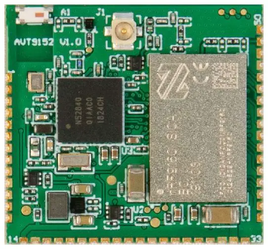
PIN ASSIGNMENTS
Edge Connector 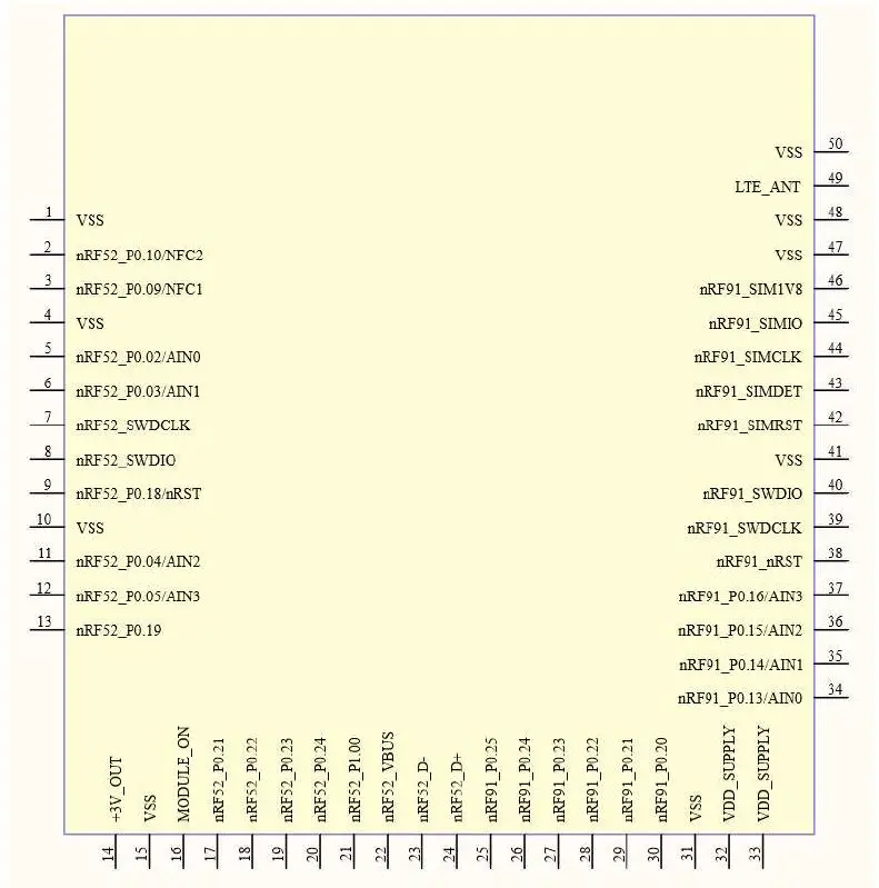
Pin Descriptions
| Pin Number | Pin Name | Pin Type | Description |
| 1 | VSS | GND | Ground |
| 2 | nRF52_P0.10/NFC2 | DIO/AI | nRF52 General-purpose digital I/O/ NFC Antenna Input |
| 3 | nRF52_P0.09/NFC1 | DIO/AI | nRF52 General-purpose digital I/O/ NFC Antenna Input |
| 4 | VSS | GND | Ground |
| 5 | nRF52_P0.02/AIN0 | DIO/AI | nRF52 General-purpose digital I/O/ Analog Input |
| 6 | nRF52_P0.03/AIN1 | DIO/AI | nRF52 General-purpose digital I/O/ Analog Input |
| 7 | nRF52_SWDCLK | DI | nRF52 Debug Port Clock |
| 8 | nRF52_SWDIO | DIO | nRF52 Debug Port Data |
| 9 | nRF52_P0.18/nRST | DIO/DI | nRF52 General-purpose digital I/O/ Reset Input (active low) |
| 10 | VSS | GND | Ground |
| 11 | nRF52_P0.04/AIN2 | DIO/AI | nRF52 General-purpose digital I/O/ Analog Input |
| 12 | nRF52_P0.05/AIN3 | DIO/AI | nRF52 General-purpose digital I/O/ Analog Input |
| 13 | nRF52_P0.19 | DIO | nRF52 General-purpose digital I/O |
| 14 | +3V_OUT | PWR | +3V, 200mA power output from module |
| 15 | VSS | GND | Ground |
| 16 | MODULE_ON | DI | Module Power On Input. Connect to VDD_SUPPLY to turn on the module, VSS to turn off the module. |
| 17 | nRF52_P0.21 | DIO | nRF52 General-purpose digital I/O |
| 18 | nRF52_P0.22 | DIO | nRF52 General-purpose digital I/O |
| 19 | nRF52_P0.23 | DIO | nRF52 General-purpose digital I/O/ Analog Input |
| 20 | nRF52_P0.24 | DIO | nRF52 General-purpose digital I/O/ Analog Input |
| 21 | nRF52_P1.00 | DIO | nRF52 General-purpose digital I/O/ Analog Input |
| 22 | nRF52_VBUS | PWR | nRF52 USB Port Power Input |
| 23 | nRF52_D- | USB | nRF52 USB negative port |
| 24 | nRF52_D+ | USB | nRF52 USB positive port |
| 25 | nRF91_P0.25 | DIO | nRF91 General-purpose digital I/O |
| 26 | nRF91_P0.24 | DIO | nRF91 General-purpose digital I/O |
| 27 | nRF91_P0.23 | DIO | nRF91 General-purpose digital I/O |
| 28 | nRF91_P0.22 | DIO | nRF91 General-purpose digital I/O |
| 29 | nRF91_P0.21 | DIO | nRF91 General-purpose digital I/O |
| 30 | nRF91_P0.20 | DIO | nRF91 General-purpose digital I/O |
| Pin Number | Pin Name | Pin Type | Description |
| 31 | VSS | GND | Ground |
| 32 | VDD_SUPPLY | PWR | 3.2V – 5V power supply to module |
| 33 | VDD_SUPPLY | PWR | 3.2V – 5V power supply to module |
| 34 | nRF91_P0.13/AIN0 | DIO/AI | nRF91 General-purpose digital I/O/ Analog Input |
| 35 | nRF91_P0.14/AIN1 | DIO/AI | nRF91 General-purpose digital I/O/ Analog Input |
| 36 | nRF91_P0.15/AIN2 | DIO/AI | nRF91 General-purpose digital I/O/ Analog Input |
| 37 | nRF91_P0.16/AIN3 | DIO/AI | nRF91 General-purpose digital I/O/ Analog Input |
| 38 | nRF91_nRST | DI | nRF91 Reset Input (active low, open collector/drain) |
| 39 | nRF91_SWDCLK | DI | nRF91 Debug Port Clock |
| 40 | nRF91_SWDIO | DIO | nRF91 Debug Port Data |
| 41 | VSS | GND | Ground |
| 42 | nRF91_SIMRST | DO | nRF91 SIM Card Reset Output |
| 43 | nRF91_SIMDET | DI | nRF91 SIM Card Presence Detect Input |
| 44 | nRF91_SIMCLK | DO | nRF91 SIM Card Clock Output |
| 45 | nRF91_SIMIO | DIO | nRF91 SIM Card Data I/O |
| 46 | nRF91_SIM1V8 | PWR | nRF91 SIM Card Power Supply (1.8V nominal) |
| 47 | VSS | GND | Ground |
| 48 | VSS | GND | Ground |
| 49 | LTE_ANT | RF | nRF91 LTE Antenna Port |
| 50 | VSS | GND | Ground |
Note: Please refer to Nordic nRF52840 and nRF9160 Datasheets and User Guides for detail function of each pin.
GPS Receiver Input Connector
A µ.FL conenctor (J1) is provided for user to connect to an external GPS antenna. J1 is connected to GPS receiver input port of nRF9160. 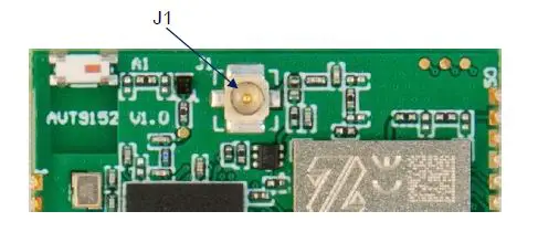
The receiver supports GPS L1/CA reception. In Nordic’s white paper “nWP033- nRF9160 Antenna and RF Interface Guidelines”, it is recommended to use active GPS antenna with LNA gain >15dB.
A 3V supply is provided to power external active GPS antenna via J1. It can be enabled via setting MAPGIO0 (pin 55 of nRF9160) to high. User may refer to “nRF91 AT Commands” for detail programming of this pin.
INTERCONNECTS BETWEEN nRF9160 AND nRF52840
Some interconnecting signals between nRF9160 and nRF52840 had been provided to aid communication/control between the 2 devices.
| nRF9160 | nRF52840 | |
| GPIOs | nRF91_P0.17 | nRF52_P0.15 |
| nRF91_P0.18 | nRF52_P0.17 | |
| nRF91_P0.19 | nRF52_P0.20 | |
| LTE Modem Coexistence Interface | nRF91_COEX0 | nRF52_P1.13 |
| nRF91_COEX1 | nRF52_P1.11 | |
| nRF91_COEX2 | nRF52_P1.15 | |
| Sub-system Reset | nRF91_nRST | nRF52_P0.13 |
| nRF91_P0.27 | nRF52_nRST | |
ABSOLUTE MAXIMUM RATINGS
| Min | Max | Unit | |
| Supply Voltage (VDD_SUPPLY) | -0.3 | 5.5 | V |
| Voltage on any Digital/Analog pin | -0.3 | 3.3 | V |
| USB Supply Voltage (nRF52_VBUS) | -0.3 | 5.8 | V |
| LTE Antenna Input RF Level | 10 | dBm | |
| GPS Antenna Input RF Level | -15 | dBm | |
| Storage temperature range | -40 | 95 | °C |
ELECTRICAL SPECIFICATIONS
Module
| Min | Typ | Max | Unit | |
| Supply Voltage (VDD_SUPPLY) | 3.2 | 3.8 | 5.0 | V |
| USB Supply Voltage (nRF52_VBUS) | 4.35 | 5 | 5.5 | V |
| Operating Temperature | -40 | 25 | 85 | °C |
LTE Modem Operation
| Min | Typ | Max | Unit | |
| Frequency Range | 699 | 2200 | MHz | |
| Max Output Power (LTE Cat-M/NB1/NB2) | 23 | dBm | ||
| Min Output Power (LTE Cat-M/NB1/NB2) | -40 | dBm | ||
| Receiver Sensitivity, Low Band (LTE Cat-M) | -103 | -108 | dBm | |
| Receiver Sensitivity, Mid Band (LTE Cat-M) | -103 | -107 | dBm | |
| Receiver Sensitivity, Low Band (LTE Cat-NB) | -108 | -114 | dBm | |
| Receiver Sensitivity, Mid Band (LTE Cat-NB) | -108 | -113 | dBm | |
| Peak Current Consumption, CAT-M1 TX sub frame, Pout=23dBm, normal operating condition | 365 | mA | ||
| Peak Current Consumption, CAT-NB1 TX sub Frame, Pout=23dBm, normal operating condition | 275 | mA | ||
| Sleep Current Consumption, CAT-M1/NB1, PSM Floor Current | 2.7 | µA |
AES-CELLIOT-AVT9152MOD
DATASHEET
| Min | Typ | Max | Unit | |
| eDRX average current, 81.92 s, one PO/PTW, PTW = 2.56 s, radio resource control (RRC) mode, Cat-M1 | 18 | µA | ||
| Average Current Cat-M1, Uplink 180 kbit/s, Pout 23 dBm, RMC settings as per 3GPP TS 36.521-1 Annex A.2, radio resource control (RRC) mode | 115 | mA | ||
| Average Current Cat-NB1, Pout 23 dBm, BPSK, 1SC, 3.75 kHz, TX 80% RX 10% (“TX intensive”), RMC settings as per 3GPP TS 36.101 Annex A.2.4, radio resource control (RRC) mode | 225 | mA |
GPS Operation
| Min | Typ | Max | Unit | |
| Acquisition Sensitivity, Cold Start | -145.5 | dBm | ||
| Acquisition Sensitivity, Hot Start | -147 | dBm | ||
| Tracking Sensitivity | -155 | dBm | ||
| Acquisition Time (Time to First Fix (TTFF)), Cold Start, Open Sky, Typical | 36 | s | ||
| Acquisition Time, Hot Start, Open Sky, Typical | 1.3 | s | ||
| Typical Peak Current, Continuous Tracking, without Power Saving Mode | 45.5 | mA | ||
| Current Consumption, Continuous Tracking, Power Saving Mode | 9.8 | mA | ||
| Average Current, Single Shot, One Fix every 2 minutes | 2.5 | mA |
Bluetooth IC Operation
| Min | Typ | Max | Unit | |
| Frequency Range | 2402 | 2480 | MHz | |
| Max Output Power | 8 | dBm | ||
| Min Output Power | -20 | dBm | ||
| Receiver Sensitivity, 1 Mbps BLE Ideal Transmitter, Packet Length ≤ 37bytes, BER=1E-320 | -95 | dBm | ||
| Transmit Current, Pout=8dBm, 1 Mbps BLE mode, Clock = HFXO, Regulator = DC/DC | 16.4 | mA | ||
| Receive Current, 1 Mbps BLE mode, Clock = HFXO, Regulator = DC/DC | 6.26 | mA |
Digital/Analog Pins
| Min | Typ | Max | Unit | |
| Interface Supply Voltage | 3.0 | V | ||
| Input High Voltage | 2.1 | 3.0 | V | |
| Input Low Voltage | 0 | 0.9 | V | |
| Output High Voltage, Standard Drive 0.5mA, High Drive 5mA | 2.6 | 3.0 | V | |
| Output Low Voltage, Standard Drive 0.5mA, High Drive 5mA | 0 | 0.4 | V |
Note: Please refer to Nordic nRF52840 and nRF9160 Datasheets and User Guides for detail characteristics and functions of nRF52840 and nRF9160.
Output Voltages
| Min | Typ | Max | Unit | |
| +3V_OUT | 2.9 | 3.0 | 3.1 | V |
| +3V_OUT Current | 0 | 200 | mA | |
| Voltage at J1 (GPS Receiver Input) | 2.9 | 3.0 | 3.1 | V |
| Output Current at J1 | 0 | 25 | mA | |
| nRF91_SIM_1V8 | 1.7 | 1.8 | 1.9 | V |
Others
| Min | Typ | Max | Unit | |
| MODULE_ON High Voltage | VDD_SUPPLY | V | ||
| MODULE_ON Low Voltage | VSS | V |
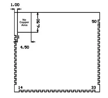
MECHANICAL SPECIFICATIONS
Mechanical Dimensions 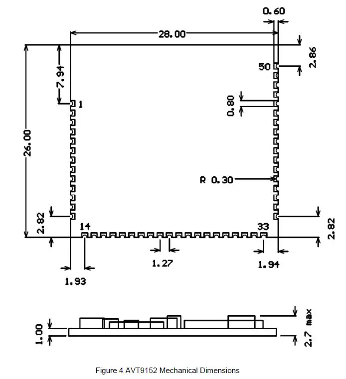 Recommended Footprint
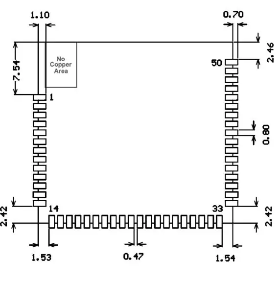
DESIGN GUIDELINES
Please take note of following guidelines when designing Host PCB:
- There should be no copper pattern at the area underneath Bluetooth SMD antenna, on all layers of PCB. Orientate the Module with the “no-copper area” at one corner of Host PCB, so that Bluetooth signal radiated from the SMD antenna is not blocked by adjacent components.

- There are some exposed test pads at bottom side of module, for internal testing purpose. Cover all patterns and via holes with soldermask on Host PCB, on the layer that is immediately below the Module, to avoid shorting with test pads above them.
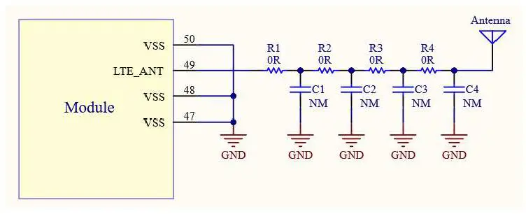
- The pin LTE_ANT on Module’s edge connector is for connection to customer’s choice of LTE antenna. The RF trace on Host PCB connecting to this pin should be of 50Ω impedance.
- If LTE antenna is not a 50Ω antenna, e.g. FPC or SMD antenna, place up to 4 segments of R-C matching network between LTE_ANT and antenna. The matching components should be placed as close to antenna as possible. Default values of R1, R2, R3 and R4 are 0Ω while C1, C2, C3 and C4 are not mounted. User can optimize their values with antenna and casing in place.

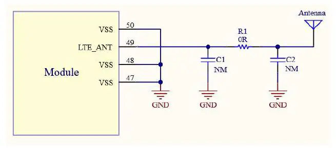
- If LTE antenna is of external swivel type, it is probably a 50Ω antenna. A π matching network (C1/R1/C2) between LTE_ANT and antenna will be adequate. The matching components should be placed as close to antenna as possible. Default values of R1 is 0Ω while C1 and C2 are not mounted. User can optimize their values with antenna and casing in place.

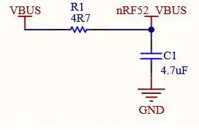
- It is recommended to include a series resistor on the USB supply for improved immunity to transient overvoltage during VBUS connection.

- nRF91_nRST is internally pulled up to 2.2V. Do not attach external pull-up resistor, or drive the pin high with voltage higher than 2.2V.
- Inside the module, there are two 100uF ceramic capacitors on VDD_SUPPLY line to cater for current surge during LTE modem operation. User can add more capacitors to VDD_SUPPLY if the battery has limited discharge current rating.
- Ensure adequate decoupling capacitors on power lines to avoid EMC issue.
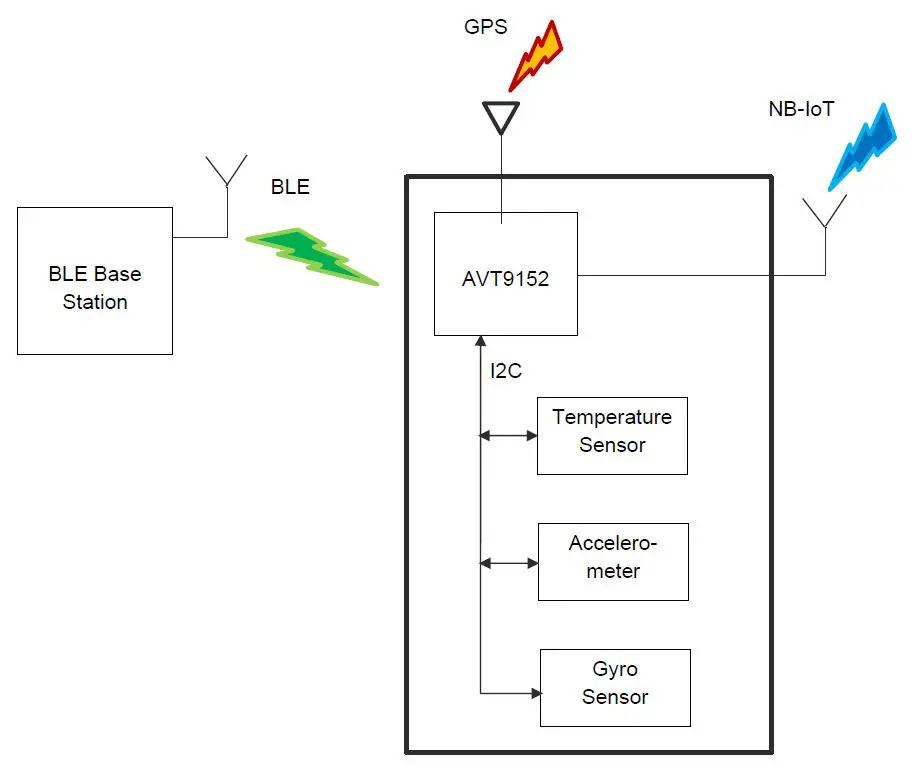
APPLICATION EXAMPLE – TRACKING DEVICE
REGULATORY INFORMATION
The product had been certified to conform with following Standards: FCC, CE, ACMA and BQB.
For certifications of LTE modem (nRF9160) with PTCRB, GCF, various local authorities and telecom operators, please refer to Nordic semiconductor’s website.
FCC
FCC ID: 2AW4N00AVT9152MOD00
Contains FCC ID: 2ANPO00NRF9160
To reuse nRF9160’s FCC ID (2ANPO00NRF9160), please observe maximum antenna gain requirement in nRF9160’s TCB report.
FCC Interference Statement
This product has been tested and found to comply with the limits for a Class B digital device, pursuant to Part 15 of the FCC Rules. These limits are designed to provide reasonable protection against harmful interference in a residential installation.
This product generates, uses, and can radiate radio frequency energy and, if not installed and used in accordance with the instructions, may cause harmful interference to radio communications. However, there is no guarantee that interference will not occur in a particular installation.
If this product does cause harmful interference to radio or television reception, which can be determined by turning the equipment off and on, the user is encouraged to try to correct the interference by one or more of the following measures:
- Reorient or relocate the receiving antenna.
- Increase the separation between the equipment and receiver.
- Connect the equipment into an outlet on a circuit different from that to which the receiver is connected.
- —Consult the dealer or an experienced radio/TV technician for help.
FCC Caution: Any changes or modifications not expressly approved by the party responsible for compliance could void the user’s authority to operate this equipment.
This device complies with Part 15 of the FCC Rules. Operation is subject to the following two conditions: (1) This device may not cause harmful interference, and (2) this device must accept any interference received, including interference that may cause undesired operation.
This device and its antenna(s) must not be co-located or operating in conjunction with any other antenna or transmitter.
IMPORTANT NOTE:
FCC Radiation Exposure Statement:
This equipment complies with FCC radiation exposure limits set forth for an uncontrolled environment. This equipment should be installed and operated with minimum distance 20cm between the radiator & your body.
This module is intended for OEM integrators under the following conditions:
- This module is certified pursuant to Part 15 rules section(15.247).
- This module is limited to host model number: AES-CELLIOT-AVT9152KIT, Brand: Avnet.
- This module has been approved to operate with the antenna types listed below, with the maximum permissible gain indicated.
Frequency Band Antenna Type Gain(dBi) 2400-2483.5MHz SMD Antenna 1.5 - Label and compliance information
Label of the end product:
The host product must be labeled in a visible area with the following “Contains FCC ID: 2AW4N00AVT9152MOD00 “.
The end product shall bear the following 15.19 statement: This device complies with part 15 of the FCC Rules. Operation is subject to the following two conditions: (1) This device may not cause harmful interference, and (2) this device must accept any interference received, including interference that may cause undesired operation. - Information on test modes and additional testing requirements
Separate approval is required for all other operating configurations, including portable configurations with respect to Part 2.1093 and different antenna configurations.
The information on how to configure test modes for host product evaluation for different operational conditions for a stand-alone modular transmitter in a host, versus with multiple, simultaneously transmitting modules or other transmitters in a host can be found at KDB Publication 996369 D04. - Additional testing, Part 15 Subpart B disclaimer
Appropriate measurements (e.g. 15B compliance) and if applicable additional equipment authorizations (e.g. SDoC) of the host product to be addressed by the integrator/manufacturer.
This module is only FCC authorized for the specific rule part 15.247 listed on the grant, and the host product manufacturer is responsible for compliance to any other FCC rules that apply to the host product as being Part 15 Subpart B compliant. - The user manual of the end product should include:
Any changes or modifications not expressly approved by the party responsible for compliance could void the user’s authority to operate this equipment.
The antenna(s) used for this transmitter must be installed to provide a separation distance of at least 20 cm from all persons.
This device complies with part 15 of the FCC Rules. Operation is subject to the following two conditions: (1) This device may not cause harmful interference, and (2) this device must accept any interference received, including interference that may cause undesired operation.
This device and its antenna(s) must not be co-located or operating in conjunction with any other antenna or transmitter.
BQB
Declaration ID: D051401
ORDER CODE
AES-CELLIOT-AVT9152MOD
STORAGE, PACKAGING AND MANUFACTURING
Storage
AVT9152 module is stored in a vacuum-sealed bag. MSL of the module is rated at 3. Storage requirements are as shown below.
- Calculated shelf life in the vacuum-sealed bag: 12 months at <40ºC and 90%RH.
- After the vacuum-sealed bag is opened, devices that will be subjected to reflow solder or other high-temperature processes must be:
- Mounted within 168 hours at a factory environment of ≤30ºC and 60%RH, or
- Stored as per J-STD-033.
- Devices require baking before mounting if any circumstance below occurs.
- When the ambient temperature is 23ºC±5ºC and the humidity indication card shows that humidity is >10% when opening the vacuum-sealed bag.
- Device mounting cannot be finished within 168 hours at factory conditions of ≤30ºC and 60%RH, or devices are not stored as per J-STD-033.
- If baking is required, refer to IPC/JEDEC J-STD-033 for the bake procedure.
Packaging
AVT9152 module is packaged in a reel of 300pcs. The diameter of reel is 330mm. There is 4 reels/CTN or 1200pcs/CTN.
Manufacturing
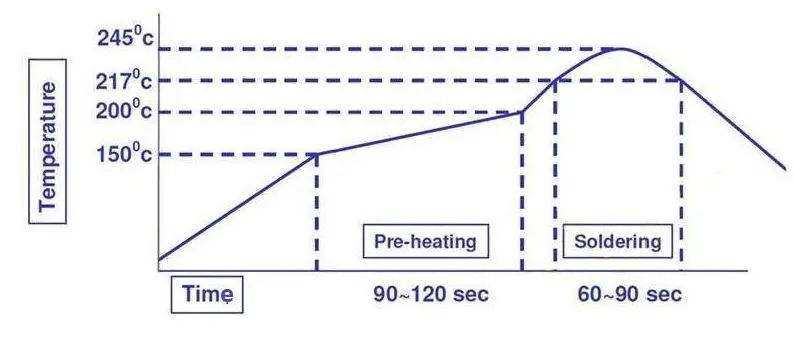
Recommended reflow profile is as shown below.