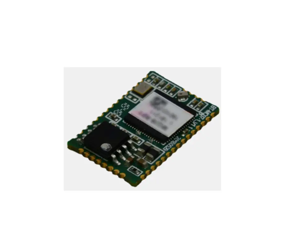
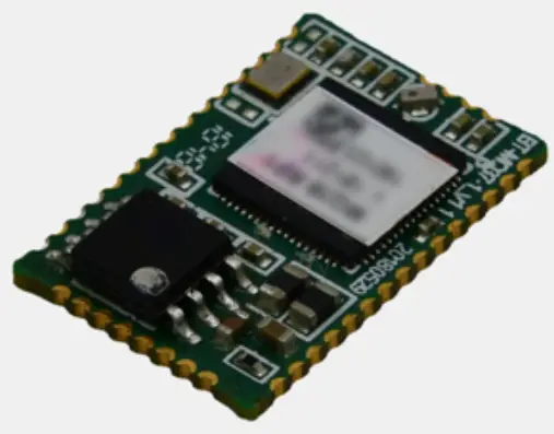
SHINWA BT-MQ38-JK1 Single Mode Bluetooth Module
Introduction
Overview
- BT-MQ38-JK1 QCC3008 BT-MQ38 -J K1 is a single mode Bluetooth module based on QCC3008 chip.BT V5.0 BDR+EDR only
- The module is a single-chip radio and baseband IC for Bluetooth 2.4GHz systems.
Features
- Support Bluetooth v5.0 specification.
- Support stereo codec and line input.
- Support 1-mic cVc hands-free NR/EC..
- Support audio transfer between carkit and mobile phone.
- Support aptX,SBC,AAC audio codecs.
- The wireless connection at distances up to 10 meters.
- Module Size: 26.8*16.8*3.2mm.
Applications
- Hands-Free Car Kits
- Wired Stereo Speakers
- Portable media players
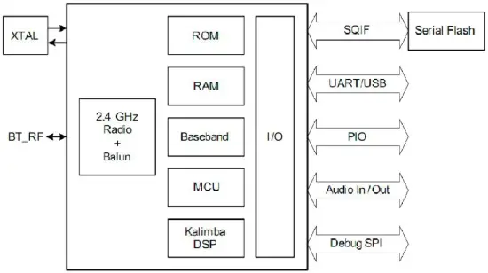
Block Diagram
Specification
General Specification
| 1 | Product Name | Bluetooth Module |
| 2 | Chip set | QCC3008 QFN |
| 3 | Power class level | Class 2 (-6dBm < PAV < 4dBm) |
| 5 | Rated Voltage | 3.3V DC(<50mVp-p) |
| 6 | Operation Voltage range | 2.8V~3.6V DC |
| 7 | Operation Distance Range | 10 meters |
| 7 | Dimension | 26.8*16.8*3.2mm (L*W*H) |
| 8 | Bluetooth Standard | Bluetooth v5.0 |
Temperature and Humidity specification
| Operation Temperature range | -40~85℃ |
| Storage Temperature range | -40~90℃ |
| Storage Humidity range | 10% ~90% |
TX Radio Specification
Items | Min. | Typ. | Max. | Unit | |
| Output transmit power | -6 | 0 | 4 | dBm | |
| Modulation characteristics | f1 avg | 140 | – | 175 | kHz |
| f2 max | 115 | – | – | kHz | |
| f2avg/f1avg | 80 | – | – | % | |
| Initial carrier-frequency tolerance | -75 | – | 75 | kHz | |
| Carrier frequency drift | DH1 | -25 | – | 25 | kHz |
| DH3 | -40 | – | 40 | kHz | |
| DH5 | -40 | – | 40 | kHz | |
| Drift rate/50us | -20 | – | 20 | kHz | |
RX Radio Specification
| Items | Min. | Max. | Unit |
| Single sensitivity(P=-70dBm) | <0.1 | % | |
| Multi sensitivity(P=-70dBm) | <0.1 | % | |
| Maximum input Level(P=-20 dBm) | <0.1 | % |
Audio Specification
| Items | Conditions | Min. | Typ. | Max. | Unit |
| Output Level (Vrms) | 1kHz,0dB | 0 | 0.3 | 0.4 | V |
| Frequency Response | 21Hz~17KHz | -3 | 0 | 3 | dB |
Design Application
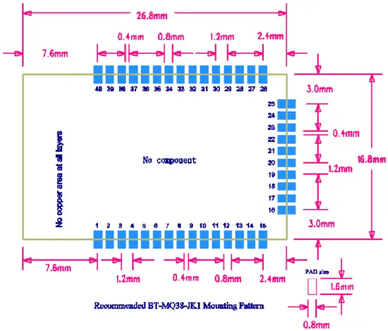
Pin Assignment
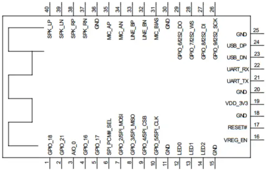
Pin Description
| No. | Pin Name | I/O | Pad type | Pin Description |
| 1 | GPIO_18 | I/O | Bidirectional with weak pull-down | Programmable input/output line18 |
| 2 | GPIO_21 | I/O | Bidirectional with weak pull-down | Programmable input/output line21 |
| 3 | AIO_0 | I | Bidirectional | Analog programmable input line 0 |
| 4 | GPIO_16 | I/O | Bidirectional with strong pull-up | Programmable input/output line16 |
| 5 | GPIO_17 | I/O | Bidirectional with strong pull-down | Programmable input/output line17 |
| 6 | SPI_PCM#_SEL | I | Input with weak pulldown | SPI/I²S select input: 0 = I²S/PIO interface 1 = SPI(for debugging) |
| 7 | GPIO_2/SPI_MOSI | I/O | Bidirectional with weak pull-down | Programmable input/output line2 -SPI_MOSI: Debug SPI data input -I2S1_SD_IN: I²S1 synchronous data input |
| 8 | GPIO_3/SPI_MISO | I/O | Bidirectional with weak pull-down | Programmable input/output line3 -SPI_MISO: Debug SPI data output -I2S1_SD_OUT: I²S1 synchronous data output |
| 9 | GPIO_4/SPI_CSB | I/O | Bidirectional with weak pull-down | Programmable input/output line4 -SPI_CS#: chip select for Debug SPI, active low -I2S1_WS: I²S1 word select |
| 10 | GPIO_5/SPI_CLK | I/O | Bidirectional with weak pull-down | Programmable input/output line5 -SPI_CLK: Debug SPI clock -I2S1_SCK: I²S1 synchronous data clock |
| 11 | GND | – | – | Ground |
| 12 | LED0 | O | Open-drain output | LED Driver |
| 13 | LED1 | O | Open-drain output | LED Driver |
| 14 | LED2 | O | Open-drain output | LED Driver |
| 15 | GND | – | – | Ground |
| 16 | VREG_EN | I | Input with internal pull-down | Regulator enable. A high input enables the on-chip regulators, which can then be latched on internally. |
| 17 | RESET# | I | Input with strong pull-up | Reset if low. Pull low for minimum 5 ms to cause a reset |
| 18 | GND | – | – | Ground |
| 19 | VDD_3V3 | I | VDD | Positive supply for Module – Supply voltage : Typical 3.3V. |
| 20 | GND | – | – | Ground |
| 21 | GPIO_1 | I/O | Bidirectional with strong pull-up | Programmable input/output line1 |
| 22 | GPIO_0 | I/O | Bidirectional with strong pull-up | Programmable input/output line0 |
| 23 | USB_DN | I/O | Bidirectional | USB data minus |
| 24 | USB_DP | I/O | Bidirectional | USB data plus with selectable internal 1.5K pull-up resistor |
| 25 | GND | – | – | Ground |
| 26 | GPIO_9 | I/O | Bidirectional with strong pull-down | Programmable input/output line9 |
| 27 | GPIO_8 | I/O | Bidirectional with strong pull-up | Programmable input/output line8 |
| 28 | GPIO_7 | I/O | Bidirectional with strong pull-down | Programmable input/output line7 |
| 29 | GPIO_6 | I/O | Bidirectional with strong pull-down | Programmable input/output line6 |
| 30 | GND | – | – | Ground |
| 31 | MIC_BIAS | O | Analog out | Microphone bias |
| 32 | LINE_BN | I | Analog in | Line input negative, channel B |
| 33 | LINE_BP | I | Analog in | Line input positive, channel B |
| 34 | MIC_AN | I | Analog in | Line or microphone input negative, channel A |
| 35 | MIC_AP | I | Analog in | Line or microphone input positive, channel A |
| 36 | GND | – | – | Ground |
| 37 | SPK_RN | O | Analog out | Speaker output negative, right |
| 38 | SPK_RP | O | Analog out | Speaker output positive, righ |
| 39 | SPK_LN | O | Analog out | Speaker output negative, left |
| 40 | SPK_LP | O | Analog out | Speaker output positive, left |
Module Outline
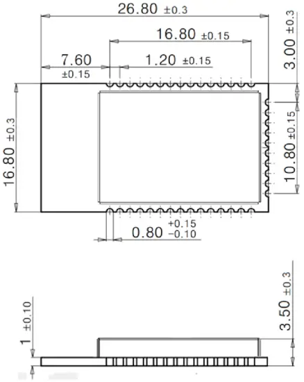
Module Dimension
Module Size:26.8*16.8*3.5mm (L*W*H)
FCC Statement
FCC standards: FCC CFR Title 47 Part 15 Subpart C Section 15.247 PCB antenna with antenna gain 0.49dBi
This device complies with part 15 of the FCC Rules.
Operation is subject to the following two conditions: (1) This device may not cause harmful interference, and (2) this device must accept any interference received, including interference that may cause undesired operation. Any Changes or modifications not expressly approved by the party responsible for compliance could void the user’s authority to operate the equipment.
Note: This equipment has been tested and found to comply with the limits for a Class B digital device, pursuant to part 15 of the FCC Rules. These limits are designed to provide reasonable protection against harmful interference in a residential installation. This equipment generates, uses and can radiate radio frequency energy and, if not installed and used in accordance with the instructions, may cause harmful interference to radio communications. However, there is no guarantee that interference will not occur in a particular installation. If this equipment does cause harmful interference to radio or television reception, which can be determined by turning the equipment off and on, the user is encouraged to try to correct the interference by one or more of the following measures:
–Reorient or relocate the receiving antenna.
–Increase the separation between the equipment and receiver.
–Connect the equipment into an outlet on a circuit different from that to which the receiver is connected.
–Consult the dealer or an experienced radio/TV technician for help.
We will retain control over the final installation of the modular such that compliance of the end product is assured. In such cases, an operating condition on the limit modular approval for the module must be only approved for use when installed in devices produced by a specific manufacturer. If any hardware modify or RF control software modify will be made by host manufacturer, C2PC or new certificate should be apply to get approval, if those change and modification made by host manufacturer not expressly approved by the party responsible for compliance ,then it is illegal.
FCC Radiation Exposure Statement
This modular complies with FCC RF radiation exposure limits set forth for an uncontrolled environment. This transmitter must not be co-located or operating in conjunction with any other antenna or transmitter. If the FCC identification number is not visible when the module is installed inside another device, then the outside of the device into which the module is installed must also display a label referring to the enclosed module. This exterior label can use wording such as the following: “Contains Transmitter Module FCC ID: ZWY3008X Or Contains FCC ID: ZWY3008X”
When the module is installed inside another device, the user manual of the host must contain below warning statements;
1. This device complies with Part 15 of the FCC Rules. Operation is subject to the following two conditions: (1) This device may not cause harmful interference. (2) This device must accept any interference received, including interference that may cause undesired operation.
Note: This equipment has been tested and found to comply with the limits for a Class B digital device, pursuant to part 15 of the FCC Rules. These limits are designed to provide reasonable protection against harmful interference in a residential installation. This equipment generates, uses and can radiate radio frequency energy and, if not installed and used in accordance with the instructions, may cause harmful interference to radio communications. However, there is no guarantee that interference will not occur in a particular installation. If this equipment does cause harmful interference to radio or television reception, which can be determined by turning the equipment off and on, the user is encouraged to try to correct the interference by one or more of the following measures:
–Reorient or relocate the receiving antenna.
–Increase the separation between the equipment and receiver.
–Connect the equipment into an outlet on a circuit different from that to which the receiver is connected.
–Consult the dealer or an experienced radio/TV technician for help.
2. Changes or modifications not expressly approved by the party responsible for compliance could void the user’s authority to operate the equipment.
The devices must be installed and used in strict accordance with the manufacturer’s instructions as described in the user documentation that comes with the product.
Any company of the host device which install this modular with modular approval should perform the test of radiated & conducted emission and spurious emission,etc. according to FCC part 15C : 15.247 and 15.209 & 15.207 ,15B Class B requirement, Only if the test result comply with FCC part 15C : 15.247 and 15.209 & 15.207 ,15B Class B requirementthen the host can be sold legally.

 Module Jdy-32 Bluetooth User Manual")


 Module User Manual")


