![]()
JS7688-core-board manual
v1.0 (2020.08.26)
Product overview
JS7688 core board module is a WIFI module based on MTK (Mediatek) MT7688AN SOC chip scheme launched by Hangzhou Jotale Technology Co., LTD.CPU frequency up to 580MHz, onboard optional 64MB DDR2 RAM/8MB Flash, 128MB DDR2 RAM/16MB Flash, 256MB DDR2 RAM/32MB Flash configuration, 150M WIFI, external leads USB 2.0 Host, GPIO, UART, I2S, I2C, SD card interface, SPI, PWM, Ethernet interface, WIFI antenna interface, etc..
This module is small in size, low in power consumption, low in heat, and stable in WIFI and network port transmission performance. Running OpenWRT (Linux) system can run stably for a long time. The peripheral circuit of the module is very simple. It only needs to add a 3.3V DC power supply to start the system and can be controlled through WIFI. The use of a gold-plated needle connection or stamp hole connection can be very stable fixed on the bottom plate.
It can be used in many applications such as smart homes, IP cameras, VOIP, remote shooting aircraft, remote monitoring systems, simple WEB network servers, simple FTP servers, remote download, remote vision cars, etc. We specially develop the motherboard for this core board, the composition JS7688 development board, and provides the detailed development information, facilitates the user to study, the development, the details please enter www.jotale.com website to view.
Product parameter
| Product name | JS7688-core-board |
| Product model | JS7688_CORE_BOARD |
| Operating system | OpenWrt (Linux) |
| CPU | MT7688AN MIPS 24KEc |
| System frequency | 580MHz |
| RAM | 64MB/128MB/256MB DDR2 RAM |
| Flash | 8MB/16MB/32MB Nor flash |
| Ethernet interface | 5 x WAN/LAN 10/100M adaptive |
| USB interface | 1 x USB 2.0 host |
| PCIE interface | 1 x PCIE |
| UART interface | UART0(debug by default), UART1, UART2 |
| GPIO interface | Total 40 (reused with other functions) |
| I2S | x 1,support VOIP |
| I2C | 1xI2C master |
| SPI master | 2 x SPI master(One of them is occupied by Flash and the other is free) |
| SPI slave | 1 x SPI slave | |
| PWM | 4 x PWM | |
| Module size | Stamp hole version | 38.5mm x 22mm x 2.8mm |
| Pin header version | 45mm x 31mm x 10mm | |
| Pin interface | Stamp hole、Pin header | |
| Operating voltage | 3.3V ±10% | |
| Average power consumption | 0.6W | |
| Supply current capacity | ≥500mA | |
| Antenna interface | 1 x IPEX | |
| Operating temperature | -20~60℃ | |
| Wireless protocol | Support IEEE802.11 b/g/n | |
| Wireless rate | 1T1R, 150Mbps | |
| RF power consumption | ≤18dbm | |
| Wireless distance | ≤100 meters (open area) | |
| Wireless working mode | routing, AP, relay, bridge | |
Appearance and pin introduction
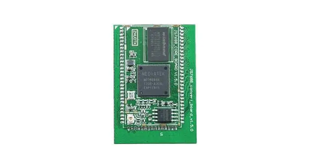
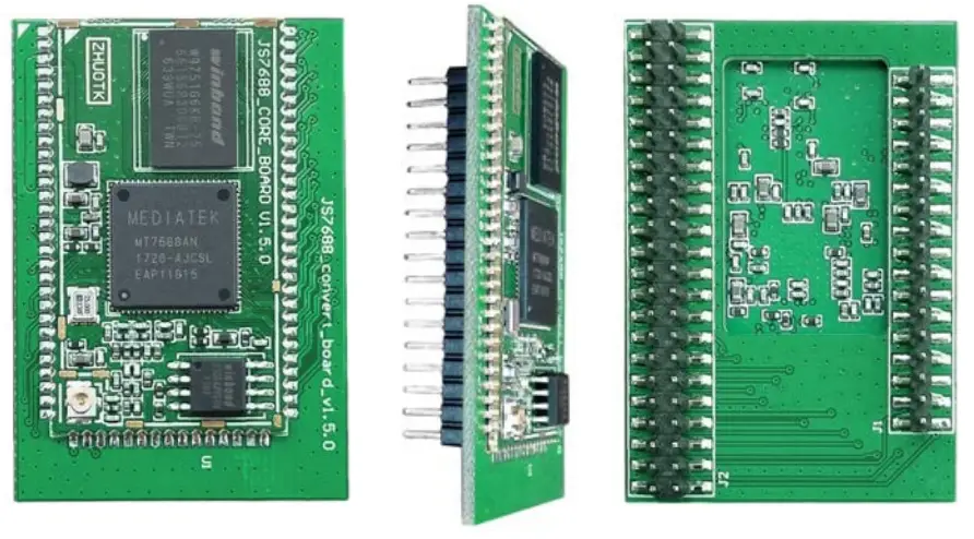
The JS7688 core board has two packaging forms available for customers to choose namely the “Stamp hole version” and “Pin header version”. Below are the photos of the real product and the packaging introduction.
2.1 Pin header version
2.1.1 Real photos
2.1.2 Pins introduction and product size
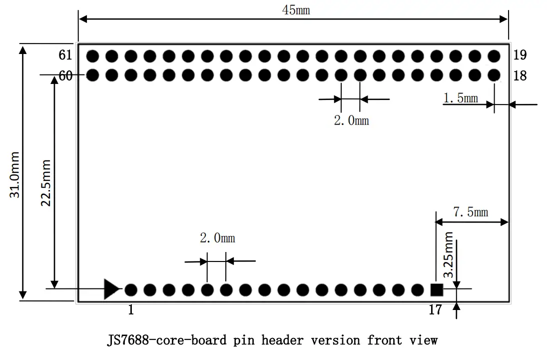
Pin introduction of JS7688-core-board pin header version
| Pin | Function 0 | Function 1 | Function 2 | Function 3 | comment |
| 1 | GND | N/A | N/A | N/A | Main power GND |
| 2 | GND | N/A | N/A | N/A | Main power GND |
| 3 | GND | N/A | N/A | N/A | Main power GND |
| 4 | VDD3V3 | N/A | N/A | N/A | Main power supply 3.3V DC |
| 5 | VDD3V3 | N/A | N/A | N/A | Main power supply 3.3V DC |
| 6 | VDD3V3 | N/A | N/A | N/A | Main power supply 3.3V DC |
| 7 | REF_CLK_O | GPIO37 | N/A | N/A | Default as GPIO, SYSTEM_LED |
| 8 | WDT_RST_N | GPIO38 | N/A | N/A | Default as GPIO, USER_KEY1 |
| 9 | EPHY_LED4_N_JTRST_N | GPIO39 | w_utif_n[6] | jtrstn_n | Default as GPIO, LAN_LED |
| 10 | EPHY_LED3_N_JTCLK | GPIO40 | w_utif_n[7] | jtclk_n | Default as GPIO, LAN2_LED |
| 11 | EPHY_LED2_N_JTMS | GPIO41 | w_utif_n[8] | jtms_n | Default as GPIO, USER_KEY2 |
| 12 | EPHY_LED1_N_JTDI | GPIO42 | w_utif_n[9] | jtdi_n | Default as GPIO, LAN1_LED |
| 13 | EPHY_LED0_N_JTDO | GPIO43 | N/A | jtdo_n | Default as GPIO, WAN_LED |
| 14 | WLED_N | GPIO44 | N/A | N/A | Default as GPIO, RESET_FN_KEY |
| 15 | GND | N/A | N/A | N/A | GND |
| 16 | UART_TXD1 | GPIO45 | PWM_CH0 | antsel[1] | Internally connect 10K pull-up resistance to 3.3V, default as UART_TXD1 |
| 17 | UART_RXD1 | GPIO46 | PWM_CH1 | antsel[0] | Default as UART_RXD1 |
| 18 | I2S_SDI | GPIO0 | PCMDRX | antsel[5] | Default as I2S_SDI |
| 19 | I2S_SDO | GPIO1 | PCMDTX | antsel[4] | Internally connect 10K pull-down resistance to GND, default as I2S_SDO |
| 20 | I2S_WS | GPIO2 | PCMCLK | antsel[3] | Default as I2S_WS |
| 21 | I2S_CLK | GPIO3 | PCMFS | antsel[2] | Default as I2S_CLK |
| 22 | I2C_SCLK | GPIO4 | sutif_txd | ext_bgclk | Default as I2C_SCLK |
| 23 | I2C_SD | GPIO5 | sutif_rxd | N/A | Default as I2C_SD |
| 24 | SPI_CS1 | GPIO6 | REF_CLK_O | N/A | Internally connect 10K pull-down resistance to GND, default as SPI_CS1 |
| 25 | VDD3V3_PROG | N/A | N/A | N/A | External Flash burner power |
| supply DC 3.3V input pin. Note: it is only necessary to connect when use the external flash burner. It is usually not connect | |||||
| 26 | SPI_CLK | GPIO7 | N/A | N/A | Internally connect 10K pull-up resistance to 3.3V, default as SPI_CLK |
| 27 | GND | N/A | N/A | N/A | GND |
| 28 | SPI_MOSI | GPIO8 | N/A | N/A | Internally connect 10K pull-down resistance to GND, default as SPI_MOSI |
| 29 | SPI_MISO | GPIO9 | N/A | N/A | Default as SPI_MISO |
| 30 | GPIO11 | GPIO11 | REF_CLK_O | PERST_N | Default as REF_CLK_O |
| 31 | SPI_CS0 | GPIO10 | N/A | N/A | Default as SPI_CS0, used by the system for flash control, can be used for flash burning |
| 32 | UART_RXD0 | GPIO13 | N/A | N/A | Default as UART_RXD0, system debug uart port |
| 33 | UART_TXD0 | GPIO12 | N/A | N/A | Internally connect 10K pull-down resistance to GND, default as UART_TXD0, system debug UART port |
| 34 | MDI_R_P0_P | N/A | N/A | N/A | Ethernet 0 receives a positive port | |
| 35 | GND | N/A | N/A | N/A | GND | |
| 36 | GND | N/A | N/A | N/A | GND | |
| 37 | MDI_R_P0_N | N/A | N/A | N/A | Ethernet 0 receives negative port | |
| 38 | MDI_T_P0_N | N/A | N/A | N/A | Ethernet 0 transmit negative port | |
| 39 | MDI_T_P0_P | N/A | N/A | N/A | Ethernet 0 transmit positive port | |
| gateway mode | IOT device mode | |||||
| 40 | MDI_T_P1_N | SPIS_CLK | GPIO15 | w_utif[1] | PWM_CH1 | Default as PWM_CH1 |
| 41 | MDI_T_P1_P | SPIS_CS | GPIO14 | w_utif[0] | PWM_CH0 | Default as PWM_CH0 |
| 42 | MDI_R_P1_N | SPIS_MOSI | GPIO17 | w_utif[3] | UART_RXD2 | Default as UART_RXD2 |
| 43 | MDI_R_P1_P | SPIS_MISO | GPIO16 | w_utif[2] | UART_TXD2 | Default as UART_TXD2 |
| 44 | MDI_R_P2_N | PWM_CH1 | GPIO19 | w_utif[5] | SD_D6 | Default as GPIO |
| 45 | MDI_R_P2_P | PWM_CH0 | GPIO18 | w_utif[4] | SD_D7 | Default as GPIO |
| 46 | GND | N/A | N/A | N/A | GND | |
| 47 | MDI_T_P2_P | UART_TXD2 | GPIO20 | PWM_CH2 | SD_D5 | Default as PWM_CH2 |
| 48 | MDI_T_P2_N | UART_RXD2 | GPIO21 | PWM_CH3 | SD_D4 | Default as PWM_CH3 |
| 49 | MDI_T_P3_P | SD_WP | GPIO22 | w_utif[10] | w_dbgin | Default as SD_WP |
| 50 | MDI_T_P3_N | SD_CD | GPIO23 | w_utif[11] | w_dbgack | Default as SD_CD |
| 51 | GND | N/A | N/A | N/A | GND | |
| 52 | MDI_R_P3_N | SD_D0 | GPIO25 | w_utif[13] | w_jtdi | Default as SD_D0 |
| 53 | MDI_R_P3_P | SD_D1 | GPIO24 | w_utif[12] | w_jtclk | Default as SD_D1 |
| 54 | GND | N/A | N/A | N/A | GND | |
| 55 | MDI_R_P4_P | SD_CLK | GPIO26 | w_utif[14] | w_jtdo | Default as |
| SD_CLK | ||||||
| 56 | MDI_R_P4_N | SD_CMD | GPIO27 | w_utif[15] | dbg_uart_t | Default as SD_CMD |
| 57 | MDI_T_P4_P | SD_D3 | GPIO28 | w_utif[16] | w_jtms | Default as SD_D3 |
| 58 | MDI_T_P4_N | SD_D2 | GPIO29 | w_utif[17] | w_jtrst_n | Default as SD_D2 |
| 59 | GND | N/A | N/A | N/A | GND | |
| 60 | USB_N | N/A | N/A | N/A | USB negative port | |
| 61 | USB_P | N/A | N/A | N/A | USB positive port | |
Note: When the chip is in “gateway mode”, the pin function of the associated network port multiplexing is unavailable. In this case, the pin function of these multiplexed pins is an ethernet port. While in “Internet of Things device mode”, the Ethernet function of these multiplexed pins is not available and other multiplexing functions are available.JS7688 pin header version and JS7628 pin header version pin is fully compatible in the common motherboard.
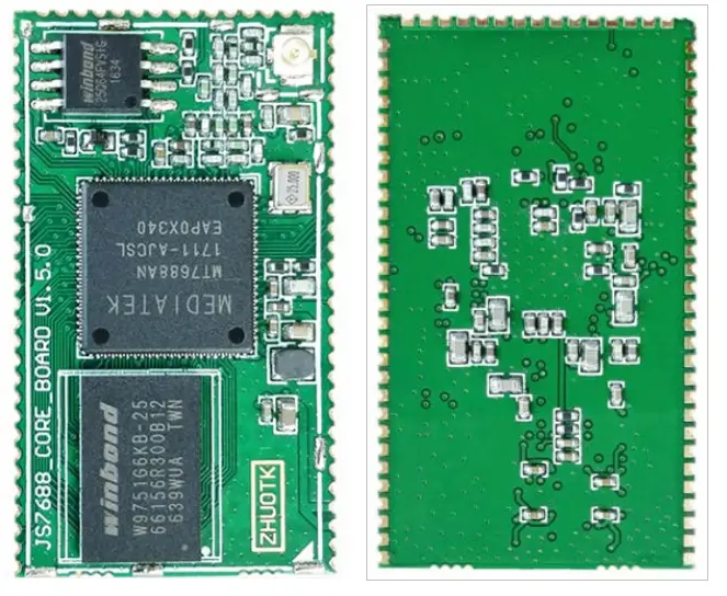
2.2 Stamp hole packaging
2.2.1 Real photos
2.2.2 Pins introduction and product size
JS7688-core-board stamp hole version pins introduction
| Pin | Function 0 | Function 1 | Function 2 | Function 3 | comment |
| 1 | GND | N/A | N/A | N/A | Main power GND |
| 2 | GND | N/A | N/A | N/A | Main power GND |
| 3 | VDD3V3 | N/A | N/A | N/A | Main power supply 3.3V DC |
| 4 | VDD3V3 | N/A | N/A | N/A | Main power supply 3.3V DC |
| 5 | GND | N/A | N/A | N/A | GND |
| 6 | PCIE_TX0_N | N/A | N/A | N/A | PCIE transmit negative port |
| 7 | PCIE_TX0_P | N/A | N/A | N/A | PCIE transmit positive port |
| 8 | GND | N/A | N/A | N/A | GND |
| 9 | PCIE_RX0_P | N/A | N/A | N/A | PCIE receive positive port |
| 10 | PCIE_RX0_N | N/A | N/A | N/A | PCIE receive negative port |
| 11 | GND | N/A | N/A | N/A | GND |
| 12 | PCIE_CK0_N | N/A | N/A | N/A | PCIE clock negative port |
| 13 | PCIE_CK0_P | N/A | N/A | N/A | PCIE clock positive port |
| 14 | PERST_N | GPIO36 | N/A | N/A | Internally connect 10K pull-down resistance to GND, |
| default as GPIO | |||||
| 15 | REF_CLK_O | GPIO37 | N/A | N/A | Default as GPIO, SYSTEM_LED |
| 16 | WDT_RST_N | GPIO38 | N/A | N/A | Default as GPIO, USER_KEY1, high level effective |
| 17 | EPHY_LED4_N_JTRST_N | GPIO39 | w_utif_n[6] | jtrstn_n | Default as GPIO, WLAN_LED |
| 18 | EPHY_LED3_N_JTCLK | GPIO40 | w_utif_n[7] | jtclk_n | Default as GPIO, LAN2_LED |
| 19 | EPHY_LED2_N_JTMS | GPIO41 | w_utif_n[8] | jtms_n | Default as GPIO, USER_KEY2, high-level effective |
| 20 | EPHY_LED1_N_JTDI | GPIO42 | w_utif_n[9] | jtdi_n | Default as GPIO, LAN1_LED |
| 21 | EPHY_LED0_N_JTDO | GPIO43 | N/A | jtdo_n | Default as GPIO, WAN_LED |
| 22 | WLED_N | GPIO44 | N/A | N/A | Default as GPIO, RESET_FN_KEY, high-level effective |
| 23 | GND | N/A | N/A | N/A | GND |
| 24 | UART_TXD1 | GPIO45 | PWM_CH0 | antsel[1] | Internally connect 10K pull-up resistance to 3.3V, default as UART_TXD1 |
| 25 | UART_RXD1 | GPIO46 | PWM_CH1 | antsel[0] | Default as UART_RXD1 |
| 26 | GND | N/A | N/A | N/A | GND |
| 27 | I2S_SDI | GPIO0 | PCMDRX | antsel[5] | Default as I2S_SDI |
| 28 | I2S_WS | GPIO2 | PCMCLK | antsel[3] | Default as I2S_WS |
| 29 | GND | N/A | N/A | N/A | GND |
| 30 | I2S_SDO | GPIO1 | PCMDTX | antsel[4] | Internally connect 10K pull-down resistance to GND, default as I2S_SDO |
| 31 | I2S_CLK | GPIO3 | PCMFS | antsel[2] | Default as I2S_CLK |
| 32 | GND | N/A | N/A | N/A | GND |
| 33 | I2C_SCLK | GPIO4 | sutif_txd | ext_bgclk | Default as I2C_SCLK |
| 34 | I2C_SD | GPIO5 | sutif_rxd | N/A | Default as I2C_SD |
| 35 | VDD3V3_PROG | N/A | N/A | N/A | External Flash burner power supply DC 3.3V |
| input pin. Note: it is only necessary to connect when use the external flash burner. It is usually not connect | |||||
| 36 | GND | N/A | N/A | N/A | GND |
| 37 | SPI_CS1 | GPIO6 | REF_CLK_O | N/A | Internally connect 10K pull-down resistance to GND, default as SPI_CS1 |
| 38 | SPI_CS0 | GPIO10 | N/A | N/A | Default as SPI_CS0,used by system for flash control, can be used for flash burning |
| 39 | SPI_MOSI | GPIO8 | N/A | N/A | Internally connect 10K pull-down resistance to GND, default as SPI_MOSI |
| 40 | SPI_CLK | GPIO7 | N/A | N/A | Internally connect 10K pull-up resistance to 3.3V, default as SPI_CLK |
| 41 | SPI_MISO | GPIO9 | N/A | N/A | Default as SPI_MISO |
| 42 | GPIO11 | GPIO11 | REF_CLK_O | PERST_N | Default as REF_CLK_O |
| 43 | UART_RXD0 | GPIO13 | N/A | N/A | Default as UART_RXD0,system debug uart port |
| 44 | UART_TXD0 | GPIO12 | N/A | N/A | Internally connect 10K pull-down resistance to GND, default as UART_TXD0, system debug uart port |
| 45 | GND | N/A | N/A | N/A | GND |
| 46 | MDI_R_P0_P | N/A | N/A | N/A | Ethernet 0 receive |
| positive port | ||||||
| 47 | MDI_R_P0_N | N/A | N/A | N/A | Ethernet 0 receives a negative port | |
| 48 | MDI_T_P0_P | N/A | N/A | N/A | Ethernet 0 transmit positive port | |
| 49 | MDI_T_P0_N | N/A | N/A | N/A | Ethernet 0 transmit negative port | |
| 50 | GND | N/A | N/A | N/A | GND | |
| gateway mode | IOT device mode | |||||
| 51 | MDI_T_P1_P | SPIS_CS | GPIO14 | w_utif[0] | PWM_CH0 | Default as PWM_CH0 |
| 52 | MDI_T_P1_N | SPIS_CLK | GPIO15 | w_utif[1] | PWM_CH1 | Default as PWM_CH1 |
| 53 | MDI_R_P1_P | SPIS_MISO | GPIO16 | w_utif[2] | UART_TXD2 | Default as UART_TXD2 |
| 54 | MDI_R_P1_N | SPIS_MOSI | GPIO17 | w_utif[3] | UART_RXD2 | Default as UART_RXD2 |
| 55 | GND | N/A | N/A | N/A | GND | |
| 56 | MDI_R_P2_P | PWM_CH0 | GPIO18 | w_utif[4] | SD_D7 | Default as GPIO |
| 57 | MDI_R_P2_N | PWM_CH1 | GPIO19 | w_utif[5] | SD_D6 | Default as GPIO |
| 58 | MDI_T_P2_P | UART_TXD2 | GPIO20 | PWM_CH2 | SD_D5 | Default as PWM_CH2 |
| 59 | MDI_T_P2_N | UART_RXD2 | GPIO21 | PWM_CH3 | SD_D4 | Default as PWM_CH3 |
| 60 | GND | N/A | N/A | N/A | GND | |
| 61 | MDI_T_P3_P | SD_WP | GPIO22 | w_utif[10] | w_dbgin | Default as SD_WP |
| 62 | MDI_T_P3_N | SD_CD | GPIO23 | w_utif[11] | w_dbgack | Default as SD_CD |
| 63 | MDI_R_P3_P | SD_D1 | GPIO24 | w_utif[12] | w_jtclk | Default as SD_D1 |
| 64 | MDI_R_P3_N | SD_D0 | GPIO25 | w_utif[13] | w_jtdi | Default as SD_D0 |
| 65 | GND | N/A | N/A | N/A | GND | |
| 66 | MDI_R_P4_P | SD_CLK | GPIO26 | w_utif[14] | w_jtdo | Default as SD_CLK |
| 67 | MDI_R_P4_N | SD_CMD | GPIO27 | w_utif[15] | dbg_uart_t | Default as SD_CMD |
| 68 | MDI_T_P4_P | SD_D3 | GPIO28 | w_utif[16] | w_jtms | Default as SD_D3 |
| 69 | MDI_T_P4_N | SD_D2 | GPIO29 | w_utif[17] | w_jtrst_n | Default as SD_D2 |
| 70 | GND | N/A | N/A | N/A | GND | |
| 71 | USB_P | N/A | N/A | N/A | USB positive port | |
| 72 | USB_N | N/A | N/A | N/A | USB negative port | |
| 73 | GND | N/A | N/A | N/A | GND | |
Note: When the chip is in “gateway mode”, the pin function of the associated network port multiplexing is unavailable. In this case, the pin function of these multiplexed pins is an ethernet port. While in “Internet of Things device mode”, the Ethernet function of these multiplexed pins is not available and other multiplexing functions are available.JS7688 pin header version and JS7628 pin header version pin fully compatible in the common motherboard.
2.2.3 Recommend package
Note: “JS7688_convert_board_xxxx.PcbLib” (XXXX is version number) JS7688 module PCB package the library is provided inside。
Baseboard reference design
3.1 Power circuit
The power supply voltage of the scoreboard is 3.3V and the average current is about 185mA. In order to ensure the stable operation of the score board, a current of at least 500mA should be reserved for the module (depending on the actual application). The figure below is the design of 3.3V power supply of JS7628 baseboard
MP1482 stabilized power supply chip is used in the figure above, which can reach 2A output current. Users can choose whether to use this model or not according to the actual situation. It is not recommended to use an “LDO chip” power supply, such as AMS1117, although the circuit design of this kind of chip is simple, the high current working efficiency is too low, and high heat, it is easy to cause the system power supply shortage, thus leading to the instability of the system.
3.2 About GPIO ports
The INPUT and output voltage of the GPIO pin of MT7628/MT7688 is 3.3V. Some GPIO pins are pull-up or pull-down inside the module to configure the system for MT7628/MT7688 startup. Note that when the board is started, the GPIO pin labeled “pull up” in the “pin introduction” should not be externally forced to pull down to a low level, and the GPIO pin labeled “pull-down” should not be externally forced to pull up to a high level, otherwise, the system may be unable to work normally. Other GPIO can be used according to the ordinary GPIO port.
3.3 Core board minimum system
The user only needs to connect the pins “GND” and “VDD3V3” of the core board to supply power to the scoreboard, and connect the three key pins “WDT_RST_N”, “EPHY_LED2_N_JTMS” and “WLED_N” with 10K pull-down resistance to the ground, and the system can work normally. This module generally does not need to add heat sinks, but in order to improve the heat dissipation efficiency of the system, please try to connect all “GND” pins of the module to the bottom plate “GND” pins designed by the reader, so as to achieve better heat dissipation effect. Other pins, such as debug serial port, network port, etc., can be added according to the user’s own needs. If you don’t need them, just not connect them. Readers can refer to“JS7628_base_board_xxxxx.pdf”(xxxxx is version number)base board schematic for designing。
The temperature when reflowing
If the customer needs to design the baseboard with the JS7688 stamp hole version module through the reflow welding machine, pay attention to the reflow welding peak emperature do not exceed 240 ℃, otherwise, it may cause damage to the JS7688 stamp hole module.
Revision history
| version | time | Modify description |
| v1.0 | 2020.08.27 | The initial version of the JS7688-core-board manual with English. Based on Chinese manual v1.6 |
FCC Statement
This device complies with part 15 of the FCC Rules. Operation is subject to the following two conditions: (1) This device may not cause harmful interference, and (2) this device must accept any interference received, including interference that may cause undesired operation. Any changes or modifications not expressly approved by the party responsible for compliance could void the user’s authority to operate the equipment.
Note: This equipment has been tested and found to comply with the limits for a Class B digital device, pursuant to part 15 of the FCC Rules. These limits are designed to provide reasonable protection against harmful interference in a residential installation. This equipment generates uses and can radiate radio frequency energy and, if not installed and used in accordance with the instructions, may cause harmful interference to radio communications. However, there is no guarantee that interference will not occur in a particular installation. If this equipment does cause harmful interference to radio or television reception, which can be determined by turning the equipment off and on, the user is encouraged to try to correct the interference by one or more of the following measures:
- Reorient or relocate the receiving antenna.
- Increase the separation between the equipment and receiver.
- Connect the equipment into an outlet on a circuit different from that to which the receiver is connected.
- Consult the dealer or an experienced radio/TV technician for help.
The WIFI Module is designed to comply with the FCC statement. FCC ID is 2AXEE-JS7688. The host system using the WIFI Module should have a label indicating it contains the modular’s FCC
ID :2AXEE-JS7688. This radio module must not be installed to colocate and operate simultaneously with other radios in the host system additional testing and equipment authorization may be required to operate simultaneously with other radios.
The WIFI module is designed for a compact PCB design.It should be installed and operated with the host or other minimum distance of 20 centimeters between the radiator and your body.” To comply with FCC regulations limiting both maximum RF output power and human exposure to RF radiation, the maximum antenna gain including cable loss in a mobile-only exposure condition must not exceed 5dBi in the 2.4G band. The WIFI Module and its antenna must not be co-located or operating in
conjunction with any other transmitter or antenna within a host device.
This module integrates an IPEX antenna interface, the user needs to purchase and install the antenna according to the instructions.
Notice to OEM integrator
The WIFI module is designed for a compact PCB design.It should be installed and operated with a laptop. OEM can install the module into the host through the module’s USB port, but it should be noted that the module’s swipe port needs to be correctly installed on the surface to ensure the normal operation of the NFC function.
The end-user manual shall include all required regulatory information/warning as shown in this manual. The OEM integrator is responsible for testing their end-product for any additional compliance requirements required with this module installed.
The device must be professionally installed The intended use is generally not for the general public.lt is generally for industry/commercial use. The connector is within the transmitter enclosure and can only be accessed by disassembly of the transmitter that is not normally required, the user has no access to the connector. Installation must be controlled. Installation requires special training This device complies with Part 15, Subpart C, Section 15.247 of the FCC Rules.
![]()
JS7688-core-board manual
Hangzhou Jotale Technology Co., Ltd
www.jotale.com


