Surenoo SLC2402A Series LCD Module User Manual

1. 54B197 ORDERING INFORMATION
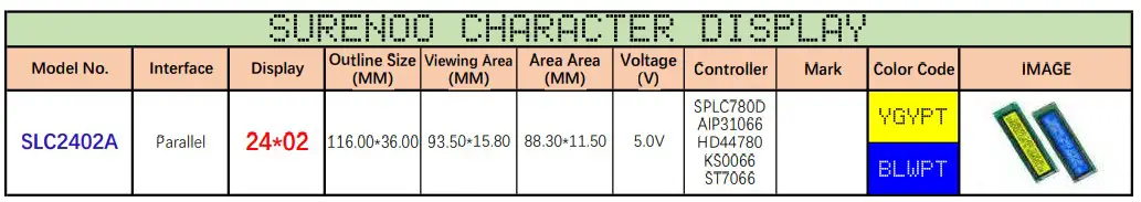
1.1 SLC2402A Series Table
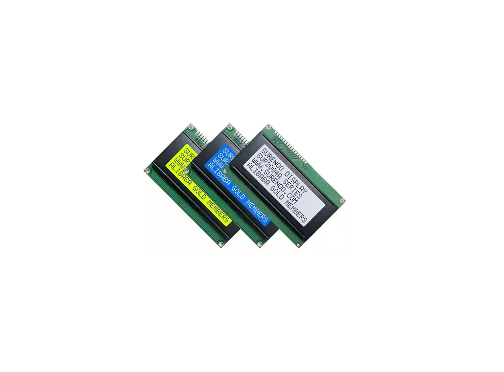
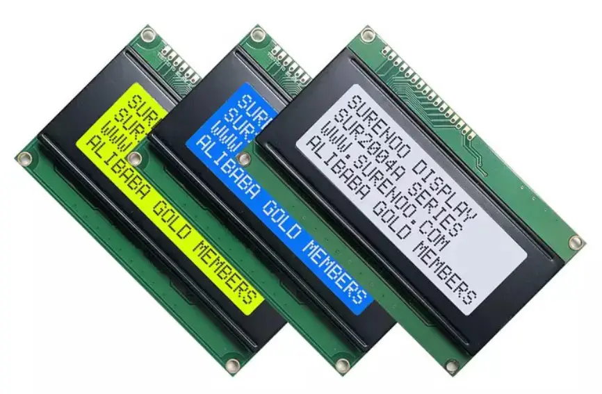
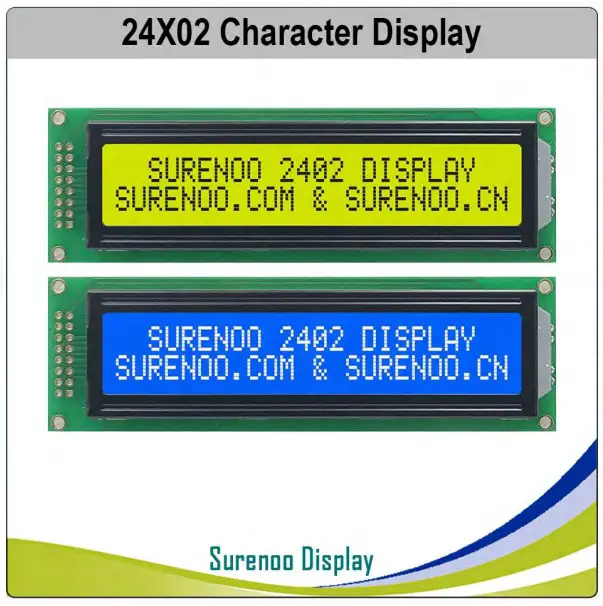
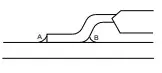
1.2 SLC2402A Series Image
- The number of series image is in accordance with number of the above series table 1.1.

2. 58B2140359B SPECIFICATION
40B5937642.1 Display Specification
| I60BT57B54B4E7B M | 6S1B58B5T5B48B ANDARD VALUE | 6U2B59B56NB49B IT |
| 6R3B60B57eB50B solution | 624B61B458B51B Characters x 2 Lines | 6-5B6-2B59B52B |
| 6D6B63B60iB6s8B play Connector | 6P7B64B6i1B6n9B Header, 16 pin | -68B6-5B62B70B |
| 7O0B67B64Bp86B erating Temperature | 7-1B628B65B807B ~ +70 | 7℃2B69B66B88B |
| 7S3B70B6t7B8o9B rage Temperature | 7-4B731B68B900B ~ +80 | 7℃5B72B69B91B |
| Touch Panel Optional | N/A | -81B7-8B75B |
| 8F2B79B7o6B nt Chip Optional | 8N3B80B77/B A | — |
2.2 Mechanical Specification
| 8I6BT83B80B EM | 8S7B84B8T1B ANDARD VALUE | 8U8B85B82NB IT |
| 8O9B86B83Butline Dimension | 910B871B84B 8.0(W) × 36.0(H) × 14.0(T) (MAX) | 9m1B88B85Bm |
| V92B89B8i6Bsual Area | 93.5(W) × 15.8(H) | m93B90B87Bm |
| 9A4B91B8c8B tive Area | 88.3(W) × 11.50(H) | m95B92B89Bm |
| Character Size | 3.20(W) × 5.55(H) | mm |
| 9D6B93B90oB83B t Size | 907B94B.91B684B 0×0.65 | 9m8B95B92Bm85B |
| 9D9B96B93oB t Pitch | 0100B97.B946B 5 ×0.70 | m101B98B95mB |
| 1N02B99B9e6B92B t Weight | 1503B1060B97B9.3B 0 ± 15% grams (typical) | 1g04B101B98B94B |
2.3 Electrical Specification
| 1I06TB103B10E0B M | 1S07B104TB101B ANDARD VALUE | 1U08B105BN102B IT |
| 1I09CB106B103B71PB ackage | 1C10B107BO104B72B B | 1-11B-108B105B |
| 1C12B109Bo106B71nB troller | 1H13B110BD107B72 44780 or Equivalent KS0066 or SPLC780 | 1-14B-111B108B |
| 1I15nB112B1t09Be95B rface | 6116B1183B110B096B 0 8-bit Parallel, 6800 4-bit Parallel | 1-17B-114B111B |
2.4 Optical Specification
| 1I19TB116B11E3B M | 1S20B117TB114B ANDARD VALUE | 1U21B118BN115B IT |
| 1L22B11C9B116B53DB Type | 1R23B120Be117B54fB er to 1.1SLC2402A Series Table | 1-24B-121B118B55B |
| 1B25B122aB119B6c5B klight Color | 1R23B120Be117B54fB er to 1.1SLC2402A Series Table | 1-27B-124B121B67B |
| 1V28B125iB12e2B62Bwing Direction | 1629B12:6B1023B63B0 | 1C30B127Bl12o4B64B ck |
| 1L31B12C8B125B56DB Duty | 1132B12/9B1126B57B6 | 1D33B130Bu127B58tB y |
| 1L34B13C1B128B59DB Bias | 1135B13/2B1529B60B | 1B36B133iB13a0B61Bs |
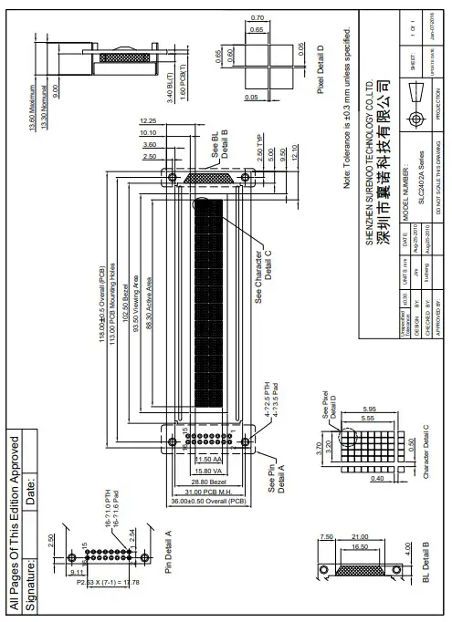
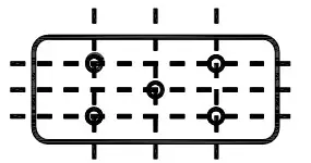
3. OUTLINE DRAWING
4. ELECTRICAL SPEC
4.1 Pin Configuration
| Pin No | Pin Name | Descriptions |
| 1 | VSS | Ground ,0V |
| 2 | VDD | Logic Power Supply |
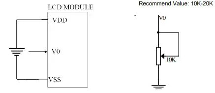
| 3 | V0 | Operating voltage for LCD |
| 4 | RS | Data / Instruction Register Select (H: Data Signal, L: Instruction Signal) |
| 5 | R/W | Read / Write (H: Read Mode, L: Write Mode) |
| 6 | E | Enable Signal |
| 7 | DB0 | Data Bit 0 |
| 8 | DB1 | Data Bit 1 |
| 9 | B2 | Data Bit 2 |
| 10 | DB3 | Data Bit 3 |
| 11 | DB4 | Data Bit 4 |
| 12 | DB5 | Data Bit 5 |
| 13 | DB6 | Data Bit 6 |
| 14 | DB7 | Data Bit 7 |
| 15 | LED_A | Backlight Anode |
| 16 up | LED_K | Backlight Cathode |
4.2 Absolute Maximum Ratings
| 433I2B5225TB12B493B02B 42E64B8B427MB245B | 2S53B250 YB247B MBOL | M254B251 B2I48BN. | 2T55B252 YB249B P. | 2M56B253 B2A50B X. | 2U57B254BN251B IT |
| 2P58B255oB252B wer Supply for Logic | 2V59B256DB253B D-VSS | -0.3 | – | +7.0 | V260B257B254BV |
| 2P61B258oB255B wer Supply for LCD | 2V62B259LB256B CD | VDD-15 | – | VDD+0.3 | V |
| 2I63nB260B2p57B ut Voltage | V264B261IB25N8B | -0.3 | – | VDD+0.3 | V |
| 2S65B262uB259B pply Current for Backlight | 2I66LB263B2E60B D | – | – | 125 | mA |
4.3 Electrical Characteristics
| 2I68TB265B26E2B M | 2S69B26 6YB263B MBOL | 2C70B26 7BO264B NDITION | M271B268 B2I65BN. | T272B26 9YB266B P. | 2M73B27 0B2A67B X. | 2U74B271 BN268B IT |
| 2P75B272oB269B wer Supply for LCM | 2V76B273DB270B D-VSS | VDD=5V | 4.8 | 5.0 | 5.2 | V |
| 2I78nB275B2p72B ut Voltage | 2V79B276IB27L3B | L Level | -0.2 | – | 1 | V |
| V282B279IB27H6B | H Level | VDD-1.0 | – | VDD | V | |
| 2L84B28C1B278B D Driving Voltage | VDD-V0 | – | 4.5 | 4.8 | 5.1 | V |
| S285B282uB279B pply Current for LCM | IDD | – | – | – | 3500.0 | uA |
| Supply Current for Backlight | ILED | – | – | 75 | – | mA |
5. INSPECTION CRITERIA
H287B41305.1 Acceptable Quality Level
28B5Each lot should satisfy the quality level defined as follows
| 2P89B286AB283B RTITION | 2A90B287BQ284B L | 2D91B288BE285B FINITION |
| 2A92B289.B286B Major | 0293B29.0B2487B % | 2F94B291uB288Bnctional defective as product |
| 2B95B292.B289B Minor | 2196B29.3B2590B % | S297B294aB291B tisfy all functions as product but not satisfy cosmetic stanard |
5.2 Definition of Lot
29B63One lot means the delivery quantity to customer at one time.
5.3 Condition of Cosmetic Inspection
301B2985◆ INSPECTION AND TEST
302B96-FUNCTION TEST
30B297-APPEARANCE INSPECTION
304B1298-PACKING SPECIFICTION
305B29◆ INSPECTION CONDITION
306B- Put under the lamp (20w¡Á2) at a distance 100mm from
307B41- Tilt upright 45 degree by the front (back) to inspect LCD appearance.
308B52◆ AQL INSPECTION LEVEL
309B6- SAMPLING METHOD: MIL-STD-105D
310B74- SAMPLING PLAN: SINGLE
31B085- MAJOR DEFECT: 0.4% (MAJOR)
312B096- MINOR DEFECT: 1.5% (MINOR)
31B07- GENERAL LEVEL: II/NORMAL
5.4 Module Cosmetic Criteria
| NO. | Item | Judgment Criterion | Partition | |||
| 1 | Difference in Spec. | None allowed | Major | |||
| 2 | Pattern Peeling | No substrate pattern peeling and floating | Major | |||
| 3 | Soldering defects | No soldering missing | Major | |||
| No soldering bridge | Major | |||||
| No cold soldering | Minor | |||||
| 4 | Resist flaw on substrate | Invisible copper foil(¢0.5mm or more)on substrate pattern | Minor | |||
| 5 | Accretion of metallic Foreign matter | No soldering dust | Minor | |||
| No accretion of metallic foreign matters(Not exceed¢0.2mm) | ||||||
| 6 | Stain | No stain to spoil cosmetic badly | Minor | |||
| 7 | Plate discoloring | No plate fading,rusting and discoloring | Minor | |||
| 8 | Solder amount 1.Lead parts | a. Soldering side of PCB
Solder to form a’Filet’ all around the lead. Solder should not hide the lead form perfectly.(too much) b.Components side (In case of ‘Through Hole PCB’)
Solder to reach the Components side of PCB | Minor | |||
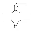
| 2.Flat packages | Either ‘toe’(A) or ‘heal’ (B) of the lead to be covered by ‘Filet
Lead form to be assume over Solder. |
A |
B | Minor | ||
| 3.Chips | (3/2) H≧h≧(1/2)H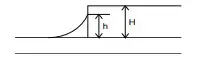 |
h |
H | Minor | ||
| 9 | Backlight defects | 1. Light fails or flickers.(Major) 2. Color and luminance do not correspond to specifications. (Major) 3. Exceeds standards for display’s blemishes, foreign matter, dark lines or scratches.(Minor) | See list ← |
| 10 | PCB defects | Oxidation or contamination on connectors.* 2. Wrong parts, missing parts, or parts not in specification.* 3.Jumpers set incorrectly.(Minor) 4.Solder(if any)on bezel,LED pad,zebra pad,or screw hole pad is not smooth.(Minor) *Minor if display functions correctly.Major if the display fails. |
See list ← |
| 11 | Soldering defects | 1. Unmelted solder paste. 2. Cold solder joints,missing solder connections,or oxidation.* 3. Solder bridges causing short circuits.* 4. Residue or solder balls. 5. Solder flux is black or brown. *Minor if display functions correctly.Major if the display fails. | Minor |
5.5 Screen Cosmetic Criteria (Non-Operating)
| No. | Defect | Judgment Criterion | Partition | |
| 1 | Spots | In accordance with Screen Cosmetic Criteria (Operating) No.1. | Minor | |
| 2 | Lines | In accordance with Screen Cosmetic Criteria (Operation) No.2. | Minor | |
| 3 | Bubbles in Polarizer | Minor | ||
| Size: d mm | Acceptable Qty in active area | |||
| d≦0.3 0.3<d≦1.0 1.0<d≦1.5 1.5<d | Disregard 3 1 0 | |||
| 4 | Scratch | In accordance with spots and lines operating cosmetic criteria, When the light reflects on the panel surface, the scratches are not to be remarkable. | Minor | |
| 5 | Allowable density | Above defects should be separated more than 30mm each other. | Minor | |
| 6 | Coloration | Not to be noticeable coloration in the viewing area of the LCD panels. Back-lit type should be judged with back-lit on state only. | Minor | |
| 7 | Contamination | Not to be noticeable. | Minor | |
5.6 Screen Cosmetic Criteria (Operating)
| No. | Defect | Judgment Criterion | Partition | |
| 1 | Spots | A) Clear | Minor | |
| Size:d mm | Acceptable Qty in active area | |||
| d≦0.1 0.1<d≦0.2 0.2<d≦0.3 0.3<d | Disregard 6 2 0 | |||
| Note: Including pin holes and defective dots which must be within one pixel Size. B) Unclear | ||||
| Size:d mm | Acceptable Qty in active area | |||
| d≦0.2 0.2<d≦0.5 0.5<d≦0.7 0.7<d | Disregard 6 2 0 | |||
| 2 | Lines | A) Clear
Note: () – Acceptable Qty in active area L – Length (mm) W -Width(mm) ∞-Disregard B) Unclear
| Minor | |
‘Clear’ = The shade and size are not changed by Vo. ‘Unclear’ = The shade and size are changed by Vo.
| No. | Defect | Judgment Criterion | Partition |
| 3 | Rubbing line | Not to be noticeable. | |
| 4 | Allowable density | Above defects should be separated more than 10mm each other. | Minor |
| 5 | Rainbow | Not to be noticeable. | Minor |
| 6 | Dot size | To be 95%~105%of the dot size (Typ.) in drawing. | Minor |
| Partial defects of each dot (ex.pin-hole) should be treated as’spot’. (see Screen Cosmetic Criteria (Operating) No.1) | |||
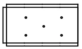
| 7 | Brightness (only back-lit Module) | Brightness Uniformity must be BMAX/BMIN≦2 – BMAX :Max.value by measure in 5 points – BMIN : Min.value by measure in 5 points Divide active area into 4 vertically and horizontally. Measure 5 points shown in the following figure.
| Minor |
| 8 | Contrast Uniformity | Contrast Uniformity must be BmAX/BMIN≦2 Measure 5 points shown in the following figure. Dashed lines divide active area into 4 vertically and horizontally. Measuring points are located at the inter-sections of dashed line.
Note: BMAX – Max.value by measure in 5 points. BMIN – Min.value by measure in 5 points. O – Measuring points in ¢10mm. | Minor |
| Note: (1) Size : d=(long length + short length)/2 (2) The limit samples for each item have priority. (3) Complexed defects are defined item by item, but if the number of defects is defined in above table, the total number should not exceed 10. | |||
4 In case of ‘concentration’, even the spots or the lines of ‘disregarded’ size should not be allowed. Following three situations
Should be treated as ‘concentration’. -7 or over defects in circle of ¢5mm. 10 or over defects in circle of ¢10mm
20 or over defects in circle of ¢20mm
6. PRECAUTIONS FOR USING
6.1 Handling Precautions
- This device is susceptible to Electro-Static Discharge (ESD) damage. Observe Anti-Static precautions.
- SUR display panel is made of glass. Do not subject it to a mechanical shock by dropping it or impact. If
- SUR display panel is damaged and the liquid crystal substance leaks out, be sure not to get any in your mouth. If the substance contacts your skin or clothes, wash it off using soap and water.
- Do not apply excessive force to the SUR display surface or the adjoining areas since this may cause the color tone to vary.
- The polarizer covering the SUR display surface of the LCD module is soft and easily scratched. Handle this polarizer carefully.
- If SUR display surface becomes contaminated, breathe on the surface and gently wipe it with a soft dry cloth. If it is heavily contaminated, moisten cloth with one of the following Isopropyl or alcohol.
- Solvents other than those above-mentioned may damage the polarizer. Especially, do not use the Water.
- Exercise care to minimize corrosion of the electrode. Corrosion of the electrodes is accelerated by water droplets, moisture condensation or a current flow in a high-humidity environment. ♦ Install the SUR LCD Module by using the mounting holes. When mounting the LCD module make sure it is free of twisting, warping and distortion. In particular, do not forcibly pull or bend the cable or the backlight cable.
- Do not attempt to disassemble or process SUR LCD module.
- NC terminal should be open. Do not connect anything.
- If the logic circuit power is off, do not apply the input signals.
- To prevent destruction of the elements by static electricity, be careful to maintain an optimum work environment. –
Be sure to ground the body when handling SUR LCD modules.
Tools required for assembling, such as soldering irons, must be properly grounded. -To reduce the amount of static electricity generated, do not conduct assembling and other work under dry conditions. –
The LCD module is coated with a film to protect the display surface. Exercise care when peeling off this protective film since static electricity may be generated.
.2 Power Supply Precautions
- Identify and, at all times, observe absolute maximum ratings for both logic and LC drivers. Note that there is some variance between models.
- Prevent the application of reverse polarity to VDD and VSS, however briefly.
- Use a clean power source free from transients. Power-up conditions are occasionally jolting and may exceed the maximum ratings of SUR modules.
- The VDD power of SUR module should also supply the power to all devices that may access the display. Don’t allow the data bus to be driven when the logic supply to the module is turned off.
6.3 Operating Precautions
- DO NOT plug or unplug SUR module when the system is powered up.
- Minimize the cable length between SUR module and host MPU.
- For models with backlights, do not disable the backlight by interrupting the HV line. Unload inverters produce voltage extremes that may arc within a cable or at the display. ♦ Operate SUR module within the limits of the modules temperature specifications.
6.4 Mechanical/Environmental Precautions
- Improper soldering is the major cause of module difficulty. Use of flux cleaner is not recommended as they may seep under the electrometric connection and cause display failure. ♦ Mount SUR module so that it is free from torque and mechanical stress.
- Surface of the LCD panel should not be touched or scratched. The display front surface is an easily scratched, plastic polarizer. Avoid contact and clean only when necessary with soft, absorbent cotton dampened with petroleum benzene.
- Always employ anti-static procedure while handling SUR module.
- Prevent moisture build-up upon the module and observe the environmental constraints for storage tem
- Do not store in direct sunlight
- If leakage of the liquid crystal material should occur, avoid contact with this material, particularly ingestion. If the body or clothing becomes contaminated by the liquid crystal material, wash thoroughly with water and soap
6.5 Storage Precautions
When storing the LCD modules, avoid exposure to direct sunlight or to the light of fluorescent lamps. Keep SUR modules in bags (avoid high temperature I high humidity and low temperatures below OC Whenever possible, SUR LCD modules should be stored in the same conditions in which they were shipped from our company.
6.6 Others
Liquid crystals solidify under low temperature (below the storage temperature range) leading to defective orientation or the generation of air bubbles (black or white). Air bubbles may also be generated if the module is subject to a low temperature. If SUR LCD modules have been operating for a long time showing the same display patterns, the display patterns may remain on the screen as ghost images and a slight contrast irregularity may also
appear. A normal operating status can be regained by suspending use for some time. It should be noted that this phenomenon does not adversely affect performance reliability. To minimize the performance degradation of the LCD modules resulting from destruction caused by static electricity etc., exercise care to avoid holding the following sections when handling the modules. -Exposed area of the printed circuit board. -Terminal electrode sections.
7. USING LCD MODULES
7.1 Liquid Crystal Display Modules
SUR LCD is composed of glass and polarizer. Pay attention to the following items when handling.
♦ Please keep the temperature within specified range for use and storage. Polarization degradation, bubble generation or polarizer peel-off may occur with high temperature and high humidity.
♦ Do not touch, push or rub the exposed polarizers with anything harder than an NB pencil lead (glass, tweezers, etc.).
♦ N-hexane is recommended for cleaning the adhesives used to attach front/rear polarizers and reflectors made of organic substances which will be damaged by chemicals such as acetone, toluene, ethanol and isopropylalcohol.
♦ When SUR display surface becomes dusty, wipe gently with absorbent cotton or other soft material like chamois soaked in petroleum benzin. Do not scrub hard to avoid damaging the display surface. ♦ Wipe off saliva or water drops immediately, contact with water over a long period of time may cause deformation or color fading.
♦ Avoid contacting oil and fats.
♦ Condensation on the surface and contact with terminals due to cold will damage, stain or dirty the polarizers. After products are tested at low temperature they must be warmed up in a container before coming is contacting with room temperature air.
♦ Do not put or attach anything on SUR display area to avoid leaving marks on.
♦ Do not touch the display with bare hands. This will stain the display area and degradate insulation between terminals (some cosmetics are determinated to the polarizers).
♦ As glass is fragile. It tends to become or chipped during handling especially on the edges. Please avoid dropping or jarring.
7.2 Installing LCD Modules
♦ Cover the surface with a transparent protective plate to protect the polarizer and LC cell.
♦When assembling the LCM into other equipment, the spacer to the bit between the LCM and the fitting plate should have enough height to avoid causing stress to the module surface, refer to the individual specifications for measurements. The measurement tolerance should be±0.1mm.
7.3 Precaution for Handling
LCD Modules Since SUR LCM has been assembled and adjusted with a high degree of precision: avoid applying excessive shocks to the module or making any alterations or modifications to it.
♦ Do not alter, modify or change the shape of the tab on the metal frame.
♦ Do not make extra holes on the printed circuit board, modify its shape or change the positions of components to be attached.
♦ Do not damage or modify the pattern writing on the printed circuit board.
♦ Absolutely do not modify the zebra rubber strip (conductive rubber) or heat seal connector.
♦ Except for soldering the interface. do not make any alterations or modifications with a soldering iron.
♦ Do not drop. bend or twist SUR LCM.
7.4 Electro-Static Discharge Control Since this module uses a CMOS LSI, the same careful attention should be paid to electrostatic discharge as for an ordinary CMOS IC.
♦ Make certain that you are grounded when handing LCM.
♦ Before remove LCM from its packing case or incorporating it into a set, be sure the module and your body have the same electric potential.
♦ When soldering the terminal of LCM. make certain the AC power source for the soldering iron does not leak.
♦ When using an electric screwdriver to attach LCM, the screwdriver should be of ground potentiality to minimize as much as possible any transmission of electromagnetic waves produced sparks coming from the commutator of the motor.
♦ As far as possible make the electric potential of your work clothes and that of the work bench the ground potential.
♦ To reduce the generation of static electricity be careful that the air in the work is not too dried. A relative humidity of 50%-60% is recommended.
7.5 Precaution for Soldering to SUR LCM
♦ Observe the following when soldering lead wire, connector cable and etc. to the LCM. -Soldering iron temperature : 280 Y.:” ± 1 0 -Soldering time: 3-4 sec. -Solder: eutectic solder. If soldering flux is used be sure to remove any remaining flux after finishing to soldering operation. (This does not apply in the case of a non-halogen type of flux.) It is recommended that you protect the LCD surface with a cover during soldering to prevent any damage due to flux spatters.
♦ When soldering the electroluminescent panel and PC board, the panel and board should not be detached more than three times. This maximum number is determined by the temperature and time conditions mentioned above, though there may be some variance depending on the temperature of the soldering iron.
♦ When remove the electroluminescent panel from the PC board, be sure the solder has completely melted. the soldered pad on the PC board could be damaged.
7.6 Precaution for Operation
♦ Viewing angle varies with the change of liquid crystal driving voltage (VO). Adjust VO to show the best contrast.
♦ Driving the SUR LCD in the voltage above the limit shortens its life.
♦ Response time is greatly delayed at temperature below the operating temperature range. However, this does not mean the LCD will be out of the order. It will recover when it returns to the specified temperature range.
♦ If SUR display area is pushed hard during operation, the display will become abnormal. However, it will return to normal if it is turned off and then back on.
♦ Condensation on terminals can cause an electrochemical reaction disrupting the terminal circuit. Therefore, it must be used under the relative condition of 40t, 50% RH.
♦ When turning the power on. input each signal after the positive/negative voltage becomes stable.
7.7 Limited Warranty
Unless agreed between SUR and customer. SUR will replace or repair any of its LCD modules which are found to be functionally defective when inspected in accordance with SUR LCD acceptance standards (copies available upon request) for a period of one year from date of shipments. Cosmetic/visual defects must be returned to SUR within 90 days of shipment. Confirmation of such date shall be based on freight documents. The warranty liability of SUR limited to repair and/or replacement on the terms set forth above. SUR will not be responsible for any subsequent or consequential events.
7.8 ReturnPolicy
No warranty can be granted if the precautions stated above have been disregarded. The typical examples of violations are: -Broken LCD glass. -PCB eyelet damaged or modified. -PCB conductors damaged. -Circuit modified in any way. including addition of components. -PCB tampered with by grinding, engraving or painting varnish. -Soldering to or modifying the bezel in any manner. Module repairs will be invoiced to the customer upon mutual agreement. Modules must be returned with sufficient description of the failures or defects. Any connectors or cable installed by the customer must be removed completely without damaging the PCB eyelet’s, conductors and terminals.


