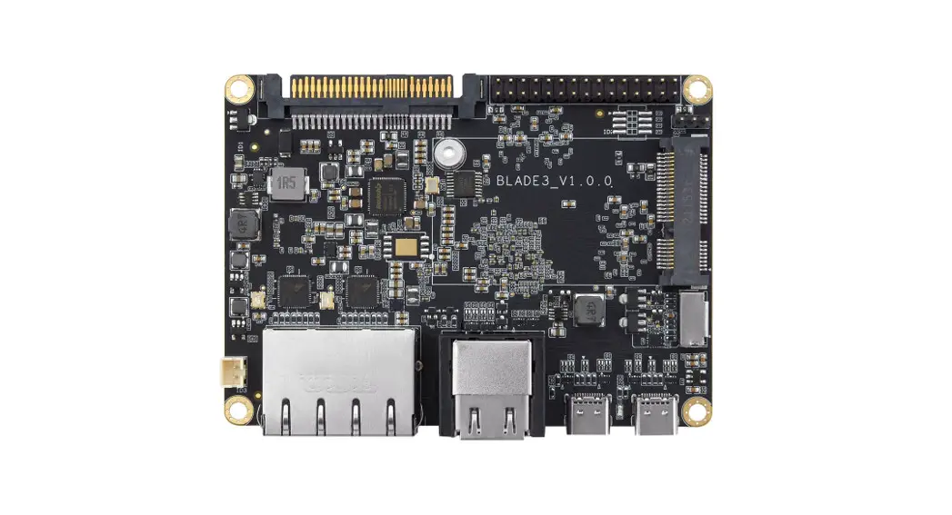
![]() Blade 3 Single Board Computer
Blade 3 Single Board Computer
User Manual
Get Started with
https://www.mixtile.com/wiki/
Changes
| Version | Date | Changes | Name |
| 1 | 2022-06-15 | First version | VT |
Introduction
1.1 Product Description
The Mixtape Blade 3 is a low-cost, low-power SBC based on the next-generation Rockchip RK3588 CPU. It allows you to cluster numerous Mix tile Blade 3 SBCs to expand your deployment, making it ideal for quick development, AI application prototyping, and edge computing.
Out-of-the-box, Mix tile Blade 3 is a stacking computer with an inbuilt PCIe Gen3 edge connector that enables the integration of many high-performance hardware platforms into a tiny form factor.
That hardware, when combined, provides a network speed of up to 20 Gb/s and a memory bandwidth of up to 136 GB/s. A Mix tile Blade 3 cluster in a 19- inch 2U chassis can support up to 600 CPU cores and 1320 GHz of processing power while requiring less than 1500 W of power.
1.2 Package list
- 1x Mix tile Blade 3 (heatsink installed)
1.3 Main Features
- CPU: Rockchip Octa-core Cortex-A76/A55 SoC processor RK3588
- NPU: Up to 6 TOPS
- Memory: Up to 32 GB LPDDR4 memory and up to 256 GB eMMC storage
- HDMI interface:
• HDMI 2.1 output (8K @ 60 FPS or 4K @ 120 FPS)
• HDMI 2.0 input (4K @ 60 FPS) - Video encoder: H.264/H.265 video encoder up to 8K @ 30 FPS
- Video decoder: H.265/H.264/VP9 video decoder up to 8K @ 60 FPS
- Display: 4-lane MIPI-CSI
- Storage expansion:
• 4-lane PCIe Gen 3 in U.2 port
• SATA 3.0 in U.2 port
• Micro-SD 3.0 flash socket - PCIe expansion: Mini-PCIe socket with PCIe Gen 2.1 and USB 2.0 support
- Ethernet expansion: Dual 2.5 gigabit Ethernet ports
- USB: Dual USB 3.2 Gen 1 Type-C ports with DisplayPort 1.4 A
- GPIOs: 30-pin GPIO socket that can be used as Digital I/O, I²C, USB 2.0, TTL UART, SPI, I²S
- Software support: Preload customized Debian 11, also support other Linux distributions and Android 12
- Power: USB Type-C Port-1 Support USB PD 2.0 protocol (Optional: 12 V DC standard SATA power in via U.2 port)
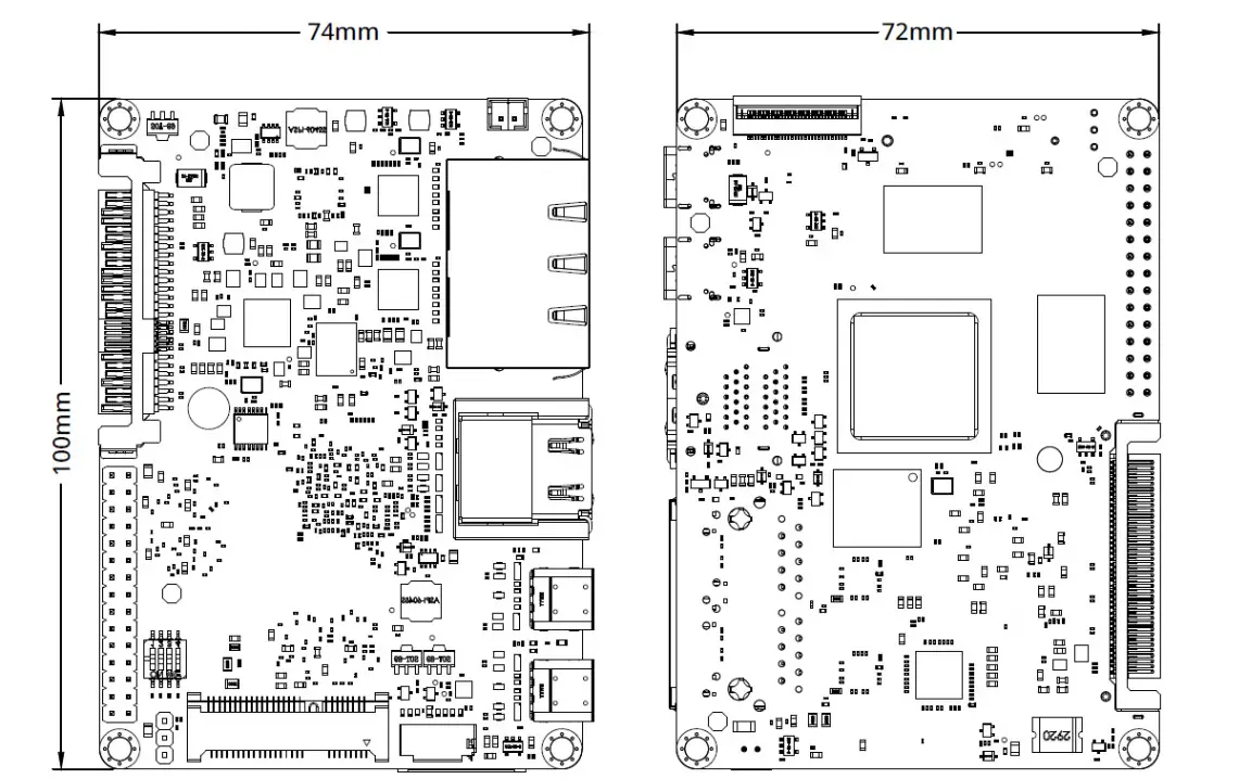
- Dimensions: 2.5-inch Pico-ITX form factor, 100 x 72 mm
- Operating temperature: 0 to +80° C
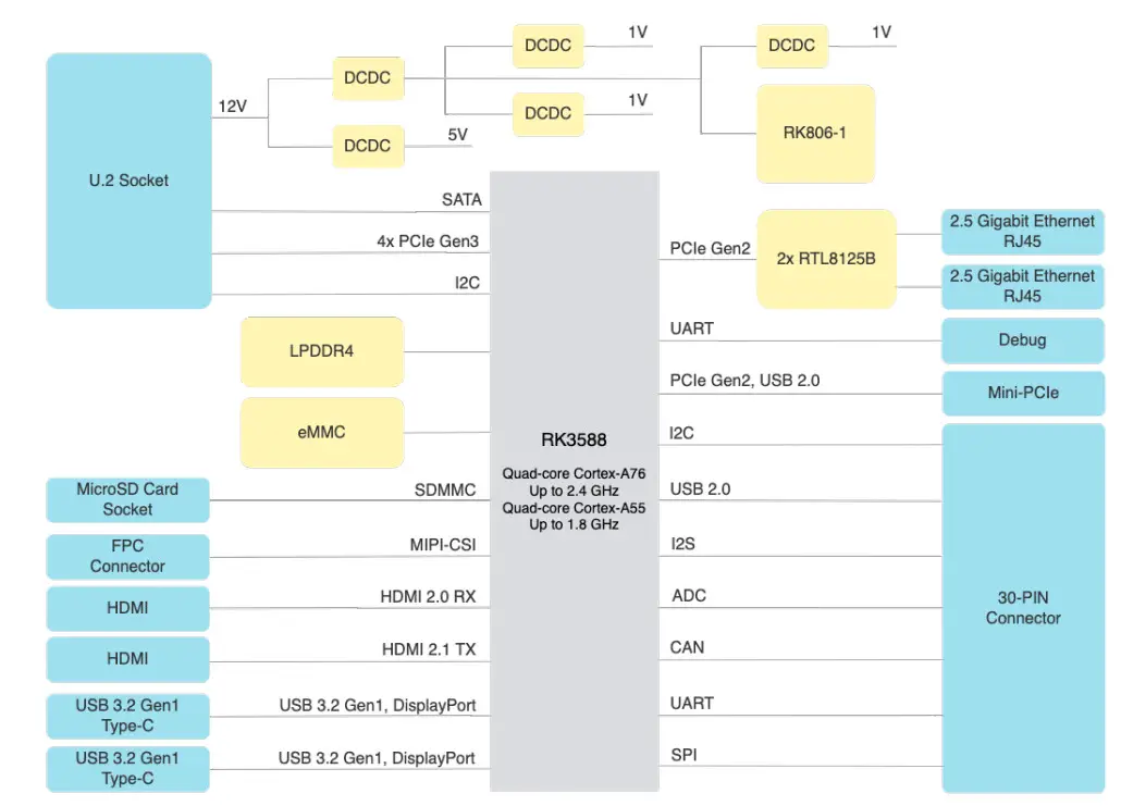
1.4 Block diagram & Product Overview
1.4.1 Block Diagram
The Block diagram for the Blade 3 single-board computer is shown below with descriptions for each function.
1.4.2 Product Overview
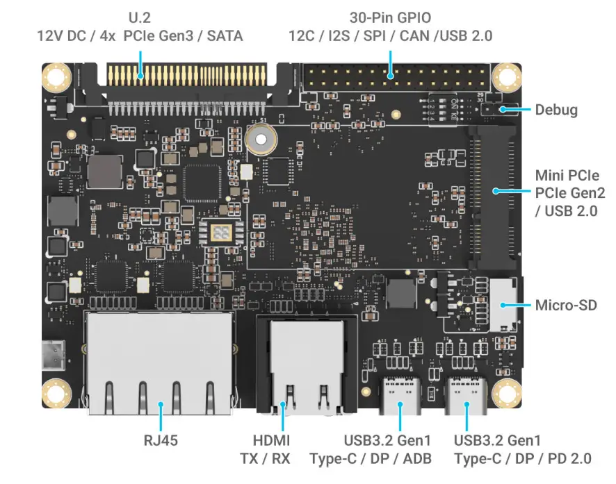
1.4.3Physical Dimensions
1.5 Key Component Specifications
The key component specifications are described below with relevant hardware information and developing notices. For more information, pin assignments and signal descriptions are listed in Chapter 2, Connectors & Pin Assignments.
1.5.1 Rockchip 3588
The Rockchip RK3588 ARM64 CPU contains many peripherals to support multi-purpose.
- Octa Cortex-A76/A55 SoC processing cores
- Core operating frequencies up to 2.4GHz
- Neural Process Unit with processing performance up to 6 TOPS
- Support 8k@60 FPS H.265/H.264/VP9 decoder; 8K@30 FPS H.264/H.265 encoder
- Supports up to 32 GB LPDDR4 memory and up to 256 GB eMMC storage
The SDRAM is 32bits data width, 4 ranks LPDDR4 memory capacities from 4GBytes to 32GBytes.
The system flash memory supports eMMC 5.1 memory capacities from 32GBytes to 256GBytes.
The default memory setting is 4/16GBytes LPDDR4 and 32/128GBytes eMMC for Blade 3.
1.5.2 MicroSD Socket
The MicroSD socket accepts standard 11mm x 15mm Micro-SD cards with capacities up to 256GBytes. The 4bits data interface supports the SDMMC3.0 protocol. While the default boot setting is the eMMC Flash which can change to the MicroSD card.
1.5.3 Mini-PCIe Socket
The mini-PCIe is a PCI card interface with a small form factor that uses a standard 52-pin mini-PCIe socket. It also contains a USB 2.0 interface.
The mini-PCIe socket supports the module sizes of 3052.
The module supporting configuration, including power, reset, and interrupt signals, is under software control by Core 3588. Since each module needs specific configuration definitions, check the configuration setting before connecting the module.
USB Support
The mini-PCIe socket supports a standard USB 2.0 interface.
1.5.4 Gigabit Ethernet
The IEEE802.3 compliant Ethernet supports auto-negotiation of 10/100/1000/2500Mb half-duplex and full-duplex. The RGMII interface from the processor connects the 2.5GbE to an external PHY, RTL8125BG-CG. The RJ45 connector has some status and speed lights. The green light indicates that you are connected, and the flashing light indicates that data is being sent. The yellow light indicates 2500Mbps and is turned off for 10/100/1000Mbps.
1.5.5 Power Input
Power Delivery (PD)
The power port is a USB-C port that supports USB Power Delivery 2.0. A Power Delivery controller on board allows for a maximum power input of 20V @ 3A.
12V DC
DC power inputs from a DC SATA power via U.2 port require 12V @ 3A.
1.5.6 USB 2.0/3.0 Host Ports
The Blade 3 features two USB Type-C ports. Both ports can support the USB-OTG capability as well as DisplayPort via USB Type-C. DisplayPort over USB Type-C enables the USB Type-C connector and cable to offer audio/video (AV) transfer via the DisplayPort interface.
It supports DisplayPort 1.4 and has a maximum resolution of 7680×4320@30Hz.
USB Type-C Port-1 supports USB PD2.0 but not USB 2.0 for ADB.
Although USB Type-C Port-0 does not support USB PD2.0, it does support USB 2.0 for ADB debugging and firmware updates.
1.5.7 Display Support
The video output processor supports the resolution from 1920×1080@60Hz to 7680×4320@60Hz.
The default main display is HDMI.
HDMI-OUT
HDMI display compliant HDMI 1.4 and HDMI 2.1 with HDCP 2.3. It supports up to 1920×1080@120Hz and 7680×4320@60Hz/3840×2160@120Hz resolution.
HDMI-IN
HDMI input compliant HDMI 1.4 and HDMI 2.0 with HDCP 2.3. It supports input sources up to 1920×1080@120Hz and 3840×2160@60Hz resolution.
1.5.8 U.2 Connector
The U.2 interface employs a 68-pin U.2 connector with a standard SATA 3.0 signal, a PCIe 3.0 X4 signal (four lanes PCIe 3.0), and 12V power input.
1.5.9 LEDs and Dip Switch
The power LED indicates the status of the power supply. There is one SPST four-position dip switch that can be used to determine the system booting mode of the Blade 3 board. Only one position can be turned ON at a time; please keep in mind that you cannot switch two positions to ON at the same time.
When position 1 is set to ON, the Blade 3 will boot from eMMC.
When position 2 is set to ON, the Blade 3 will boot from the MicroSD card.
When position 3 is turned ON, the Blade 3 will boot from SPI Flash.
When position 4 is activated, Blade 3 enters MaskROM mode for firmware development.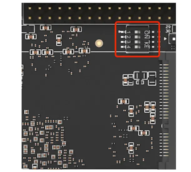
Connectors & Pin Assignments
The following section lists the interface connector pin assignments and pin types with corresponding signal descriptions. The interface connectors on Blade 3 are listed in the table below.
2.1 30-Pin Connector
| Pin # | Pin Name | Pin Type | Input/Output | Signal Description |
| 1 | VCC_SVO | Power | Output | Power supply for USB,5V output MAX 500mA. |
| 2 | GND | Power | NA | Power and signal reference ground. |
| 3 | USB2O_HOSTO_DM | LVDS | BI | USB20 HOST PortO Data Minus |
| 4 | I2S2_SDI_M1 | signal | Input | 1252 data input |
| 5 | USB2O_HOSTO_DP | LVDS | BI | USB20 HOST Port() Data Plus |
| 6 | I2S2_SDO_M1 | signal | Output | I2S2 data output |
| 7 | GND | Power | NA | Power and signal reference ground. |
| 8 | 1252_MCLK_M1 | signal | Output | I2S2 Master clock |
| 9 | I2C5_SDA_M3 | signal | EH | I2C5 Bus Date |
| 10 | I2S2_SCLK_M1 | signal | BI | 1252 serial clock or BCLK |
| 11 | I2C5_SCL_M3 | signal | Output | I2C5 Bus clock |
| 12 | I2S2_LRCK_Ml | signal | BI | 1252 Left/Right channel clock |
| 13 | GND | Power | NA | Power and signal reference ground. |
| 14 | GND | Power | NA | Power and signal reference ground. |
| 15 | SPI4_MISO_M2 | signal | Input | SPI4 Master input,Slave output |
| 16 | CAN2_RX | signal | Input | CAN2 receive data |
| 17 | SPI4_MOSI_M2 | signal | Output | SPI4 Master output, Slave input |
| 18 | CAN2_TX | signal | Output | CAN2 transmit data |
| 19 | SPI4_CLK_M2 | signal | Output | SPI4 clock |
| 20 | GND | Power | NA | Power and signal reference ground. |
| 21 | SPI4_CSO_M2 | signal | Output | SPI4 Chip Select 0 |
| 22 | GPIOO_BO | signal | BI | GPIO bank 0 port BO |
| 23 | GPIOLA4 | signal | BI | GPIO bank 1 port A4 |
| 24 | SARADC_VIN7 | Analog | Input | SAR AX Channel 7 input |
| 25 | GND | Power | NA | Power and signal reference ground. |
| 26 | SARADC_VIN6 | Analog | Input | SAR AX Channel 6 input |
| 27 | PWM14 | signal | BI | Pulse Width Modulation 14 input or output |
| 28 | GND | Power | NA | Power and signal reference ground. |
| 29 | PWM15 | signal | BI | Pulse Width Modulation 15 input or output |
| 30 | VCC_3V330 | Power | Output | Power supply for peripheral, 3.3V output MAX 500mA. |
2.2 Fan Connector
| Pin # | Pin Name | Pin Type | Input/Output | Signal Description |
| 1 | VCC5V_FAN | Power | Output | Power supply for FAN,5V output MAX 400mA.Control by GPI03_CO |
| 2 | GND | Power | NA | Power reference ground. |
2.3 Mini-PCIe
| Pin # | Pin Name | Pin Type | Input/Output | Signal Description |
| 1 | MINIPCIE2O_WAKEN_3V3_L | signal | Input | Wake-up the signal from the mini-PCIe device |
| 2 | VCC3V3_MINIPCIE | Power | Output | Power supply for the mini-PCIe device,3.3V output MAX 3A in all pins |
| 3 | NC | float | NA | No connected to this pin |
| 4 | GND | Power | NA | Power and signal reference ground. |
| 5 | NC | float | NA | No connected to this pin |
| 6 | NC | float | NA | No connected to this pin |
| 7 | MINIPCIE2O_CLKREQN_3V3_L | signal | Input | PCIe2.0 Channel Reference clock request |
| 8 | NC | float | NA | No connected to this pin |
| 9 | GND | Power | NA | Power and signal reference ground. |
| 10 | NC | float | NA | No connected to this pin |
| 11 | PCIE20_2_REFCLKN | LVDS | Output | PCIe20 Port2 differential clock Negative |
| 12 | NC | float | NA | No connected to this pin |
| 13 | PCIE20_2_REFCLKP | LVDS | Output | PCIe20 Port2 differential clock Positive |
| 14 | NC | float | NA | No connected to this pin |
| 15 | GND | Power | NA | Power and signal reference ground. |
| 16 | NC | float | NA | No connected to this pin |
| 17 | NC | float | NA | No connected to this pin |
| 18 | GND | Power | NA | Power and signal reference ground. |
| 19 | NC | float | NA | No connected to this pin |
| 20 | W_DISABLEN | signal | Output | PCI-E device wireless disable |
| 21 | GND | Power | NA | Power and signal reference ground. |
| 22 | MINIPCIE2O_PERSTN | signal | Output | PCI-E devise reset |
| 23 | PCIE20_2_RXN | LVDS | Input | PCIe20 receives differential Negative |
| 24 | VCC3V3_MINIPCIE | Power | Output | Power supply for the mini-PCIe device,3.3V output MAX 3A in all pins |
| 25 | PCIE20_2_RXP | LVDS | Input | PCIe20 receives differential Positive |
| 26 | GND | Power | NA | Power and signal reference ground. |
| 27 | GND | Power | NA | Power and signal reference ground. |
| 28 | NC | float | NA | No connected to this pin |
| 29 | GND | Power | NA | Power and signal reference ground. |
| 30 | NC | float | NA | No connected to this pin |
| 31 | MINIPCIE2O_TX_N | LVDS | Output | PCIe20 transmit differential Negative |
| 32 | NC | float | NA | No connected to this pin |
| 33 | MINIPCIE2O_TX_P | LVDS | Output | PCIe20 transmit differential Positive |
| 34 | GND | Power | NA | Power and signal reference ground. |
| 35 | GND | Power | NA | Power and signal reference ground. |
| 36 | MINIPCIE_USB_DM | LVDS | BI | USB20 HOST Portal Data Minus |
| 37 | GND | Power | NA | Power and signal reference ground. |
| 38 | MINIPCIE_USB_DP | LVDS | BI | USB20 HOST Portal Data Plus |
| 39 | VCC3V3_MINIPCIE | Power | Output | Power supply for the mini-PCIe device,3.3V output MAX 3A in all pins |
| 40 | GND | Power | NA | Power and signal reference ground. |
| 41 | VCC3V3_MINIPCIE | Power | Output | Power supply for the mini-PCIe device,3.3V output MAX 3A in all pins |
| 42 | NC | float | NA | No connected to this pin |
| 43 | GND | Power | NA | Power and signal reference ground. |
| 44 | NC | float | NA | No connected to this pin |
| 45 | NC | float | NA | No connected to this pin |
| 46 | NC | float | NA | No connected to this pin |
| 47 | NC | float | NA | No connected to this pin |
| 48 | NC | float | NA | No connected to this pin |
| 49 | NC | float | NA | No connected to this pin |
| 50 | GND | Power | NA | Power and signal reference ground. |
| 51 | NC | float | NA | No connected to this pin |
| 52 | VCC3V3_MINIPCIE | Power | Output | Power supply for the mini-PCIe device,3.3V output MAX 3A in all pins |
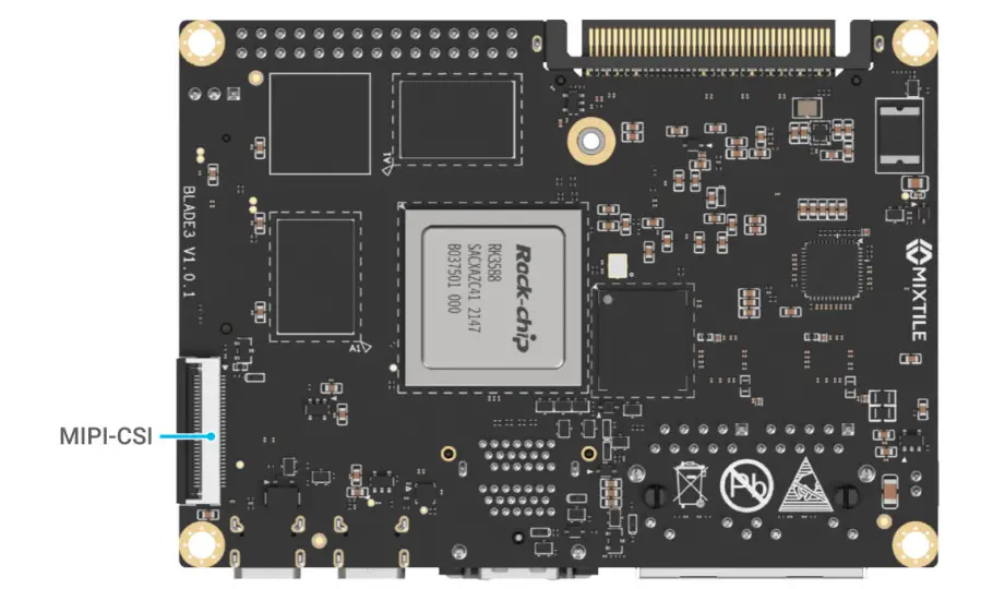
2.4 MIPI-CSI
| Pin # | Pin Name | Pin Type | Input/Output | Signal Description |
| 1 | GND | Power | NA | Power and signal reference ground. |
| 2 | MIPI_CSIO_RX_DON | LVDS | Input | MIPI CSIO receives differential data lane 0 Negative |
| 3 | MIPI_CSIO_RX_DOP | LVDS | Input | MIPI CSIO receives differential data lane 0 Positive |
| 4 | GND | Power | NA | Power and signal reference ground. |
| 5 | MIPI_CSIO_RX_D1N | LVDS | Input | MIPI CSIO receives differential data lane 1 Negative |
| 6 | MIPI_CSIO_RX_D1P | LVDS | Input | MIPI CSIO receives differential data lane 1 Positive |
| 7 | GND | Power | NA | Power and signal reference ground. |
| 8 | MIPI_CSIO_RX_CLKON | LVDS | Input | MIPI CSIO receives differential Clock 0 Negativ€ |
| 9 | MIPI_CSIO_RX_CLKOP | LVDS | Input | MIPI CSIO receives differential Clock 0 Positive |
| 10 | GND | Power | NA | Power and signal reference ground. |
| 11 | MIPI_CSIO_RX_D2N | LVDS | Input | MIPI CSIO receives differential data lane 2 Negative |
| 12 | MIPI_CSIO_RX_D2P | LVDS | Input | MIPI CSIO receives differential data lane 2 Positive |
| 13 | GND | Power | NA | Power and signal reference ground. |
| 14 | MIPI_CSIO_RX_D3N | LVDS | Input | MIPI CSIO receives differential data lane 3 Negative |
| 15 | MIPI_CSIO_RX_D3P | LVDS | Input | MIPI CSIO receives differential data lane 3 Positive |
| 16 | GND | Power | NA | Power and signal reference ground. |
| 17 | MIPI_CAM_PWM2 | signal | Output | PWM2 for LENS |
| 18 | NC | float | NA | No connected to this pin |
| 19 | VCC_3V3_S0 | Power | Output | Power supply for sensor board,3.3V output |
| 20 | MIPI_CAM_RESETN | signal | Output | GPIO out for sensor reset |
| 21 | NC | float | NA | No connected to this pin |
| 22 | MIPI_CAM_PDN | signal | Output | GPIO out for sensor power down |
| 23 | I2C3_SDA_M3_MIPI | signal | Ill | I2C5 Bus data |
| 24 | I2C3_SCL_M3_MIPI | signal | Output | I2C5 Bus clock |
| 25 | GND | Power | NA | Power and signal reference ground. |
| 26 | MIPI_CAM2_CLK_M1_3V3 | signal | Output | Camera Master clock output |
| 27 | GND | Power | NA | Power and signal reference ground. |
| 28 | VCC_SVO | Power | Output | Power supply for sensor board, SV output |
| 29 | VCC_SVO | Power | Output | Power supply for sensor board, SV output |
| 30 | VCC_SVO | Power | Output | Power supply for sensor board, SV output |
2.5 U.2
| Pin# | Pin Name | Pin Type | Input/Output | Signal Description |
| El | PCIE30 REFCLKP SLOT | LVDS | Output | RC PCIe30 differential clock Positive |
| E2 | PCIE3O_REFCLKN_SLOT | LVDS | Output | RC PCIe30 differential clock Negative |
| E3 | VCC_3V3_SO | Power | Output | Power supply for JO |
| E4 | PCIE30X4 CLKREQN_Ml_L | signal | Output | DM PCIe30 Channel Reference clock request |
| E5 | PCIE30X4 PERSTN_MUL | signal | Input | DM PCIe30 Channel reset |
| E6 | PCIE30X4 CLKREQN_M3 | signal | Input | RC PCIe30 Channel Reference clock request |
| E7 | PCIE30 PORT1 REFCLKP | LVDS | Input | DM PCIe30 differential clock Positive |
| E8 | PCIE3O_PORTl_REFCLKN | LVDS | Input | DM PCIe30 differential clock Negative |
| E9 | GND | Power | NA | Power and signal reference ground. |
| E10 | PCIE3O_PORTl_TX2P | LVDS | Output | DM PCIe30 transmit differential Positive |
| E11 | PCIE30 PORT1 TX2N | LVDS | Output | DM PCIe30 transmit differential Negative |
| E12 | GND | Power | NA | Power and signal reference ground. |
| E13 | PCIE30 PORT1 RX2N | LVDS | Input | DM PCIe30 receives differential Negative |
| E14 | PCIE30 PORT1 RX2P | LVDS | Input | DM PCIe30 receives differential Positive |
| E15 | GND | Power | NA | Power and signal reference ground. |
| E16 | NC | float | NA | No connected to this pin |
| E17 | PCIE30 PORTO RX1P | LVDS | Input | RC PCIe30 receives differential Negative |
| E18 | PCIE30 PORTO RX1N | LVDS | Input | RC PCIe30 receives differential Positive |
| E19 | GND | Power | NA | Power and signal reference ground. |
| E20 | PCIE30 PORTO TX1N | LVDS | Output | RC PCIe30 transmit differential Positive |
| E21 | PCIE30 PORTO TX1P | LVDS | Output | RC PCIe30 transmit differential Negative |
| E22 | GND | Power | NA | Power and signal reference ground. |
| E23 | I2C4 SCL MO | signal | Output | I2C4 Bus clock |
| E24 | I2C4 SDA MO | signal | BI | I2C4 Bus data |
| E25 | DUALPORT_EN# | signal | Output | GPIO for Enable dual port, default low |
| P1 | PCIE30X4_WAKEN_M l_L | signal | Output | DM PCIE30 Wake-up signal from RC |
| P2 | PCIE30X4_WAKEN_M3 | signal | Input | RC PCIE30 Wake up the signal from DM |
| P3 | PWRDIS | signal | Output | GPIO for power disable to device |
| P4 | IFDET | signal | Input | GPIO for detecting the interface of the device |
| P5 | GND | Power | NA | Power and signal reference ground. |
| P6 | GND | Power | NA | Power and signal reference ground. |
| P7 | NC | float | NA | No connected to this pin |
| P8 | NC | float | NA | No connected to this pin |
| P9 | NC | float | NA | No connected to this pin |
| P10 | PRSNT# | signal | Input | GPIO for detecting device if present |
| P11 | ACTIVITY# | signal | Input | GPIO for detecting device if the activity |
| P12 | GND | Power | NA | Power and signal reference ground. |
| P13 | U2_12V | Power | Input | Power supply for blade3, input 12V |
| P14 | U2_12V | Power | Input | Power supply for blade3, input 12V |
| P15 | U2_12V | Power | Input | Power supply for blade3, input 12V |
| S1 | GND | Power | NA | Power and signal reference ground. |
| S2 | SATAO TXP | LVDS | Output | SATA30 Port() transmit differential Positive |
| S3 | SATAO TXN | LVDS | Output | SATA30 Port() transmit differential Negative |
| S4 | GND | Power | NA | Power and signal reference ground. |
| S5 | SATAO RXN | LVDS | Input | SATA30 Port() receive differential Positive |
| S6 | SATAO RXP | LVDS | Input | SATA30 Port() receive differential Negative |
| S7 | GND | Power | NA | Power and signal reference ground. |
| S8 | GND | Power | NA | Power and signal reference ground. |
| S9 | NC | float | NA | No connected to this pin |
| S10 | NC | float | NA | No connected to this pin |
| S11 | GND | Power | NA | Power and signal reference ground. |
| S12 | NC | float | NA | No connected to this pin |
| S13 | NC | float | NA | No connected to this pin |
| S14 | GND | Power | NA | Power and signal reference ground. |
| S15 | PCIE30X4_PERSTN_M3 | signal | Output | RC PCIe30 Channel reset |
| S16 | GND | Power | NA | Power and signal reference ground. |
| 517 | PCIE30 PORTl_TX3P | LVDS | Output | DM PCIe30 transmit differential Negative |
| 518 | PCIE30 PORTl_TX3N | LVDS | Output | DM PCIe30 transmit differential Positive |
| 519 | GND | Power | NA | Power and signal reference ground. |
| S20 | PCIE30 PORT1 RX3N | LVDS | Input | DM PCIe30 receives differential Negative |
| S21 | PCIE30 PORT1 RX3P | LVDS | Input | DM PCIe30 receives differential Positive |
| S22 | GND | Power | NA | Power and signal reference ground. |
| S23 | PCIE30 PORTO RXOP | LVDS | Input | RC PCIe30 receives differential Negative |
| S24 | PCIE30 PORTO RON | LVDS | Input | RC PCIe30 receives differential Positive |
| S25 | GND | Power | NA | Power and signal reference ground. |
| S26 | PCIE30 PORTO_TXON | LVDS | Output | RC PCIe30 transmit differential Negative |
| S27 | PCIE30 PORTO_TXOP | LVDS | Output | RC PCIe30 transmit differential Positive |
| S28 | GND | Power | NA | Po+A137:E196wer and signal reference ground. |
2.6 Debug
| Pin# | Pin Name | Pin Type | Input/Output | Signal Description |
| 1 | UART2_RX_MO_DEBUG | signal | Input | UART2 Receive Data for debug |
| 2 | UART2_TX_MO_DEBUG | signal | Output | UART2 Transmit Data for debug |
| 3 | GND | signal | NA | Signal reference ground. |
Specifications
3.1 Environmental
| Parameter | Specifications |
| Operating Temperature | 0 ° to +80 °C |
| Storage Temperature | 0 ° to +80 °C |
3.2 Mechanical
| Parameter | Specifications |
| 2.5-inch Pico-ITX | 100 x 72mm |
| Weight | 160g |
Support
4.1 Technical Support
MIX TILE technical support team assists you with the questions you may have. Contact us with the following methods below.
Email: [email protected]
Website: https://www.mixtile.com


